Article

Applying ZCT to Two-Phase Boost Converter with IGBT Switches Used

Department of Electrical Engineering, National Taipei University of Technology, 1, Sec. 3, Zhongxiao E. Rd., Taipei 10608, Taiwan
*
Author to whom correspondence should be addressed.
Micromachines 2022, 13(12), 2055; https://doi.org/10.3390/mi13122055
Submission received: 3 October 2022 / Revised: 15 November 2022 / Accepted: 19 November 2022 / Published: 24 November 2022

Abstract

:
A zero-current-transition (ZCT) strategy is proposed herein. This strategy is applied to a two-phase boost converter with isolated gate bipolar transistors (IGBTs) used as main switches. However, IGBTs have a current tail during the switch-off interval. Consequently, the proposed constant-frequency ZCT strategy along with common-ground auxiliary switches is employed to decrease the switching loss generated by the current tail. Furthermore, the light-load efficiency can be upgraded by regulating the switch-off instants and switch-on times of the two auxiliary switches. Moreover, two phases are interleaved with one phase having a phase difference of 180° from the other phase, and controlled by a current-sharing controller so that the input current can be distributed between the two phases as evenly as possible. Moreover, only one current sensing circuit is required to obtain information on currents in the two main switches. Above all, the number of phases can be extended with easy control of the ZCT and current balance.

1. Introduction

In recent years, due to the impact of the energy crisis, power supply products must have several features, such as power saving, stability and small size, etc. To meet these features, switching power supply will become the trend in power supply development in the future. However, due to the parasitic inductance and parasitic capacitance of the power switch elements in the traditional switching power supply, the power switch will cause switching loss under operation [1]. In addition, if the insulated gate bipolar transistor (IGBT) is used as a power switch, the current tail during the turn-off period will increase the switching loss.
Based on the above, the literature [2,3,4] uses the resonant zero-current switching (ZCS) technique to reduce the switching loss due to hard switching, but the corresponding power switch must withstand extremely high resonant currents, thereby increasing the conduction loss. In addition, since the resonant inductor and the resonant capacitor have a fixed execution time, the ZCS technique requires the use of variable frequency control, so the filter is not easy to design. In the literature [5,6,7,8,9], ZCS techniques with pulse width modulation (PWM) are used. Although this PWM ZCS technique has improved the problem of increased conduction loss and difficulty in filter design, the power switch is still subjected to extremely high resonant inductor currents. In addition, there are many additional components used in [9].
To conquer the shortcomings of the PWM ZCS technique, the zero-current transition (ZCT) [10,11,12] can be realized by fixed frequency control and does not need to increase the current stress of the power switch, thereby reducing the conduction loss and making the filter design easy. In [12], there is a floating auxiliary switch used.
In the following, more papers with a ZCT turn-off are described. The literature [13] starts with the introduction of the conventional ZCT converter. The advantage of this circuit is that it can realize the ZCT turn-off of the main switch without increasing the voltage stress of the main switch, but the disadvantage is that the main switch is hard-switched during the turn-on period, increasing the current stress of the main switch, while the auxiliary switch is also hard-switched during the turn-on and -off period. In [14], a novel improvement is provided by putting a ZCT auxiliary circuit on the secondary side of the circuit, so that the main switch can achieve a ZCT turn-off, although the main switch has no additional current stress during the turn-on period, but on the contrary, the main switch has additional current stress during the turn-off period. The main switch in [15] has no additional current stress during the turn-on period, but the drawback is that the auxiliary switch is floating, which increases the design difficulty of the drive circuit to some extent. In [16], an upgraded method is used to direct the inductive energy that causes the auxiliary switch to have additional voltage stress to the output side through the transformer, and both the main switch and auxiliary switch can achieve a ZCT turn-off, which makes the efficiency improve effectively, but the demerit is that the circuit is complex and has too many switching elements, which increases the difficulty of circuit analysis. In [17], although the circuit is simple and there is no additional current stress on the main switch during the turn-on period, the disadvantage is that the voltage stress on the main switch and auxiliary switch is too large, which requires the use of high voltage withstanding IGBTs and hence increases the cost.
On the other hand, many power supply products nowadays take multiphase interleaved control [18,19,20] to increase the output power. However, the line impedance of each phase is not equal. Consequently, it is necessary to add current sharing control [21,22,23] to distribute the load current evenly in each phase. Furthermore, since the current sharing control should sample the current of each phase, a traditional multi-phase interleaved power supply should have a current sampling circuit for each phase to feedback the current signal of each phase so that the load current can be equally distributed in each phase.
In this paper, we propose a two-phase interleaved boost converter with main IGBT switches having the ZCT turn-on by using the proposed auxiliary circuits, along with the proposed current sensing technique. The basic operating principle and mathematical deduction for the proposed topology are described in detail, then its feasibility is evaluated by the IsSpice software, and finally, a physical prototype, with the FPGA chip utilized as a system control kernel, is provided to demonstrate its effectiveness.

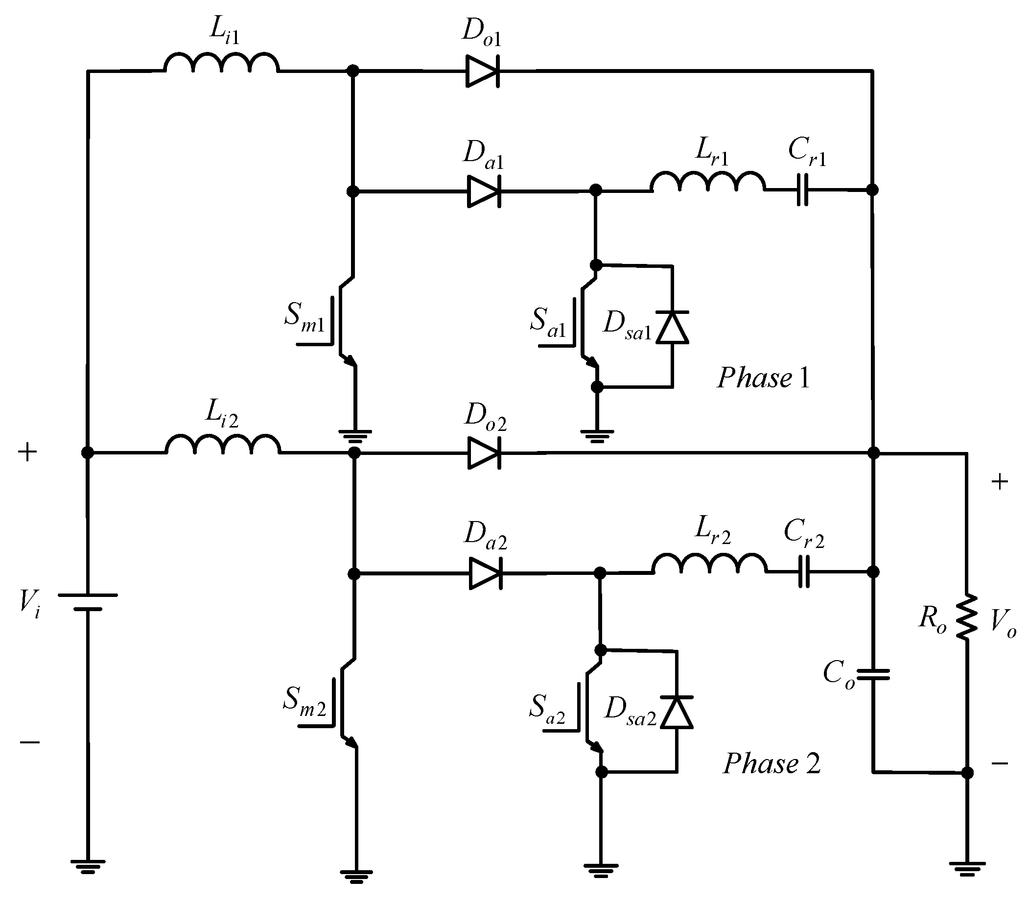
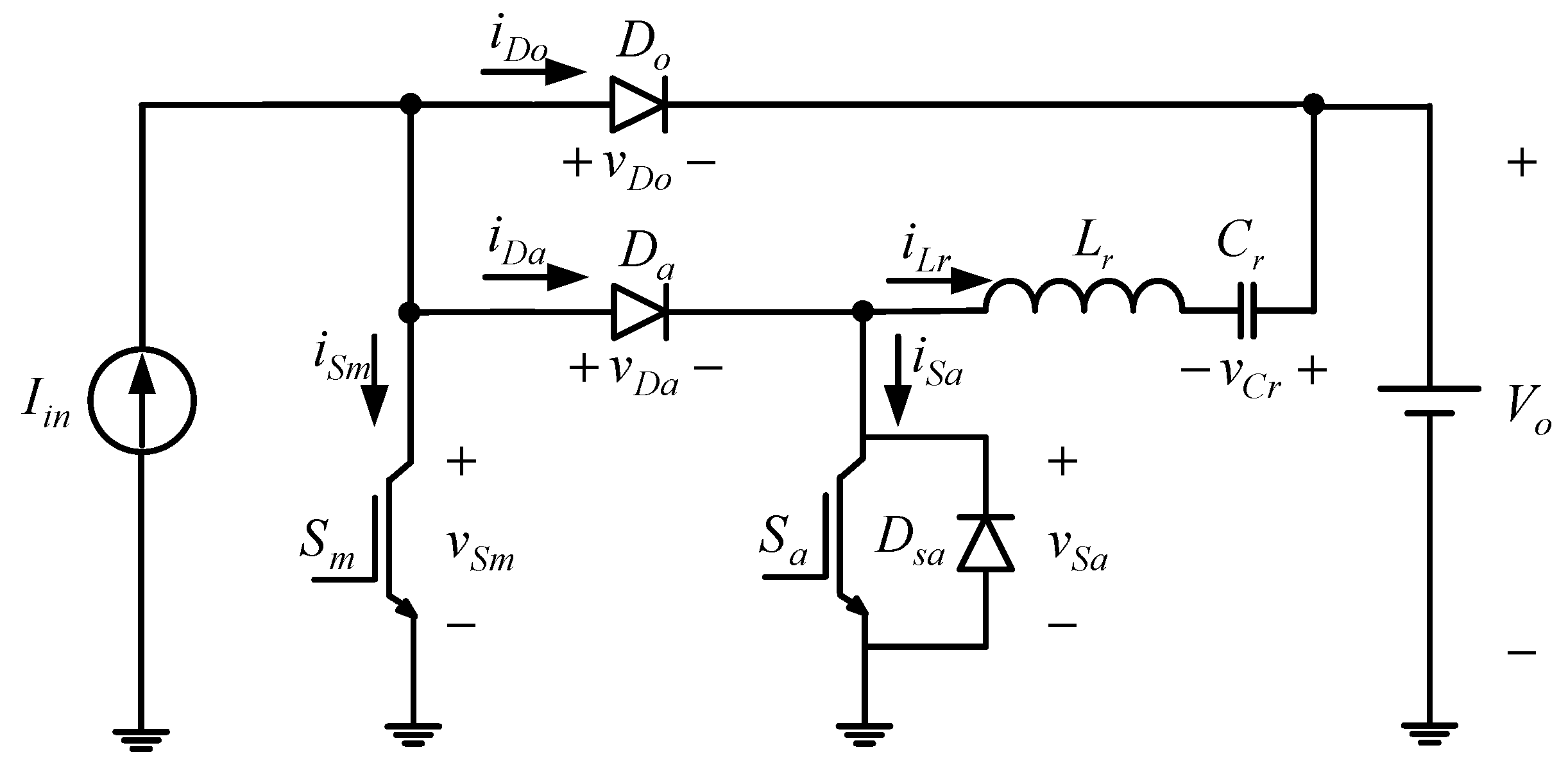
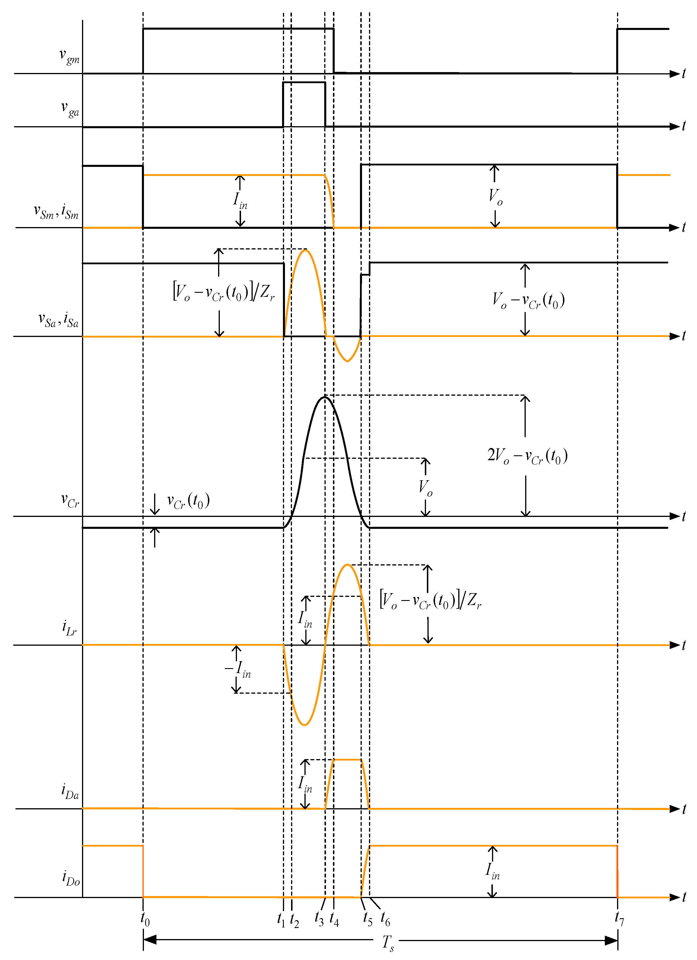
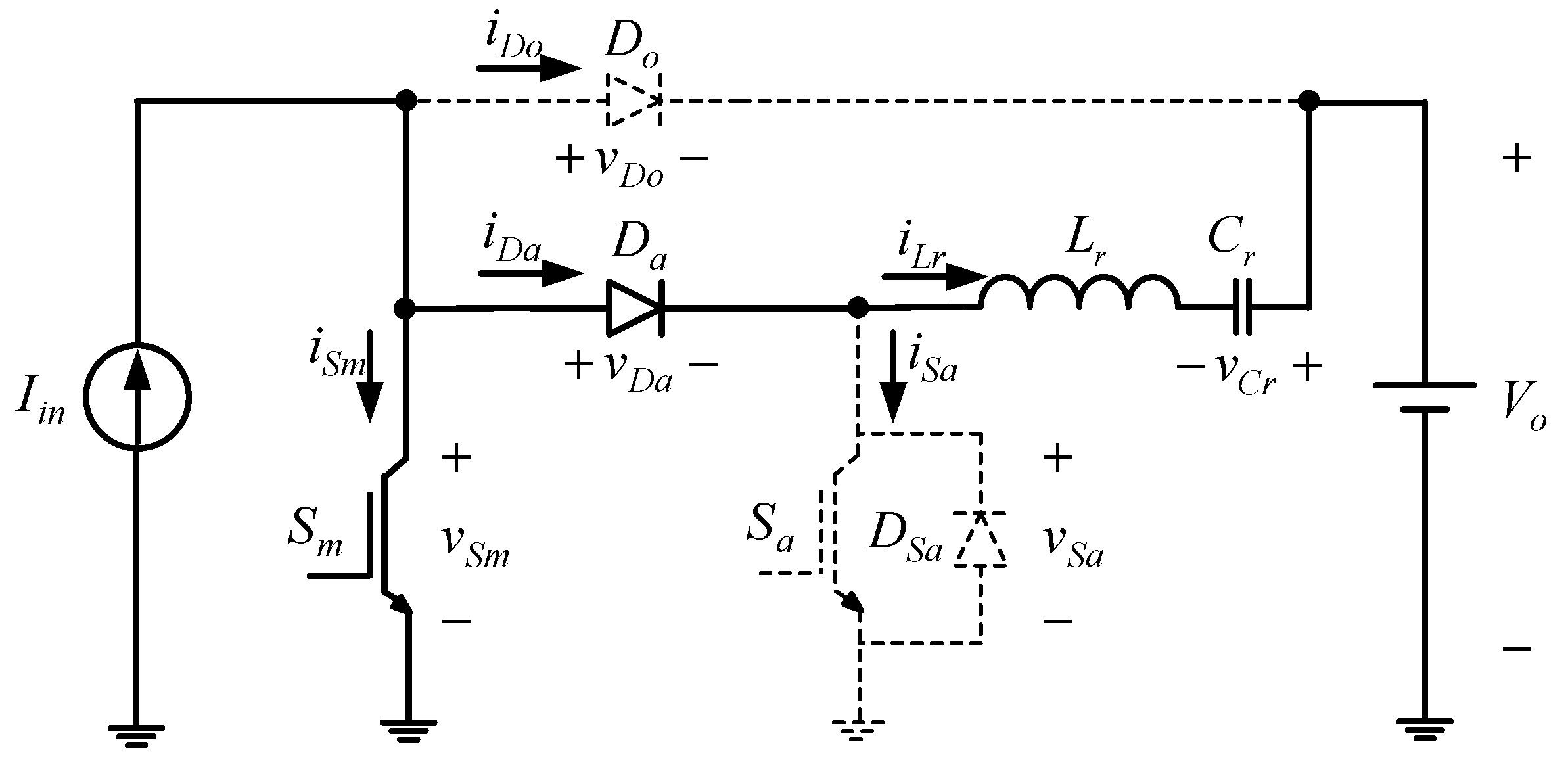
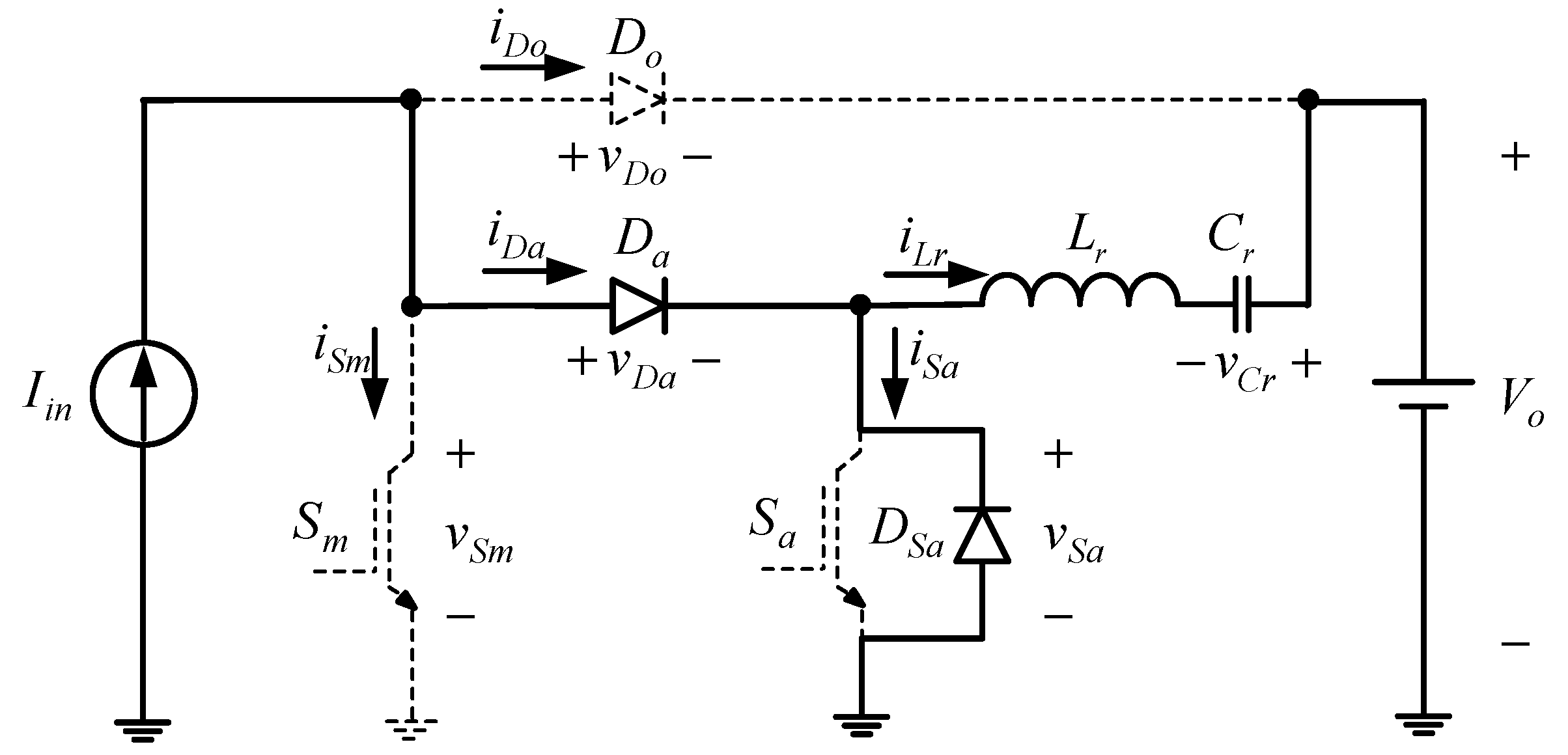
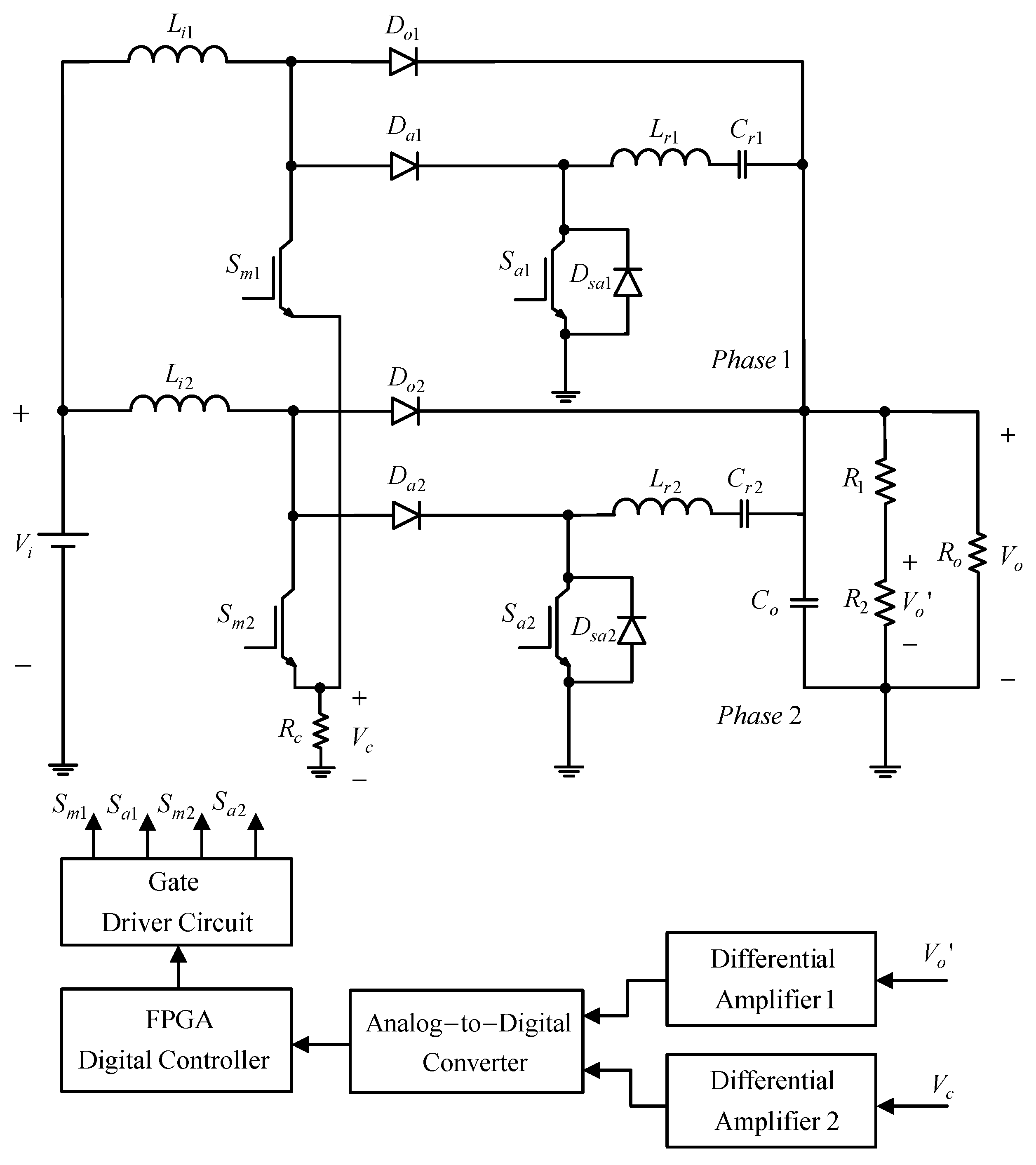
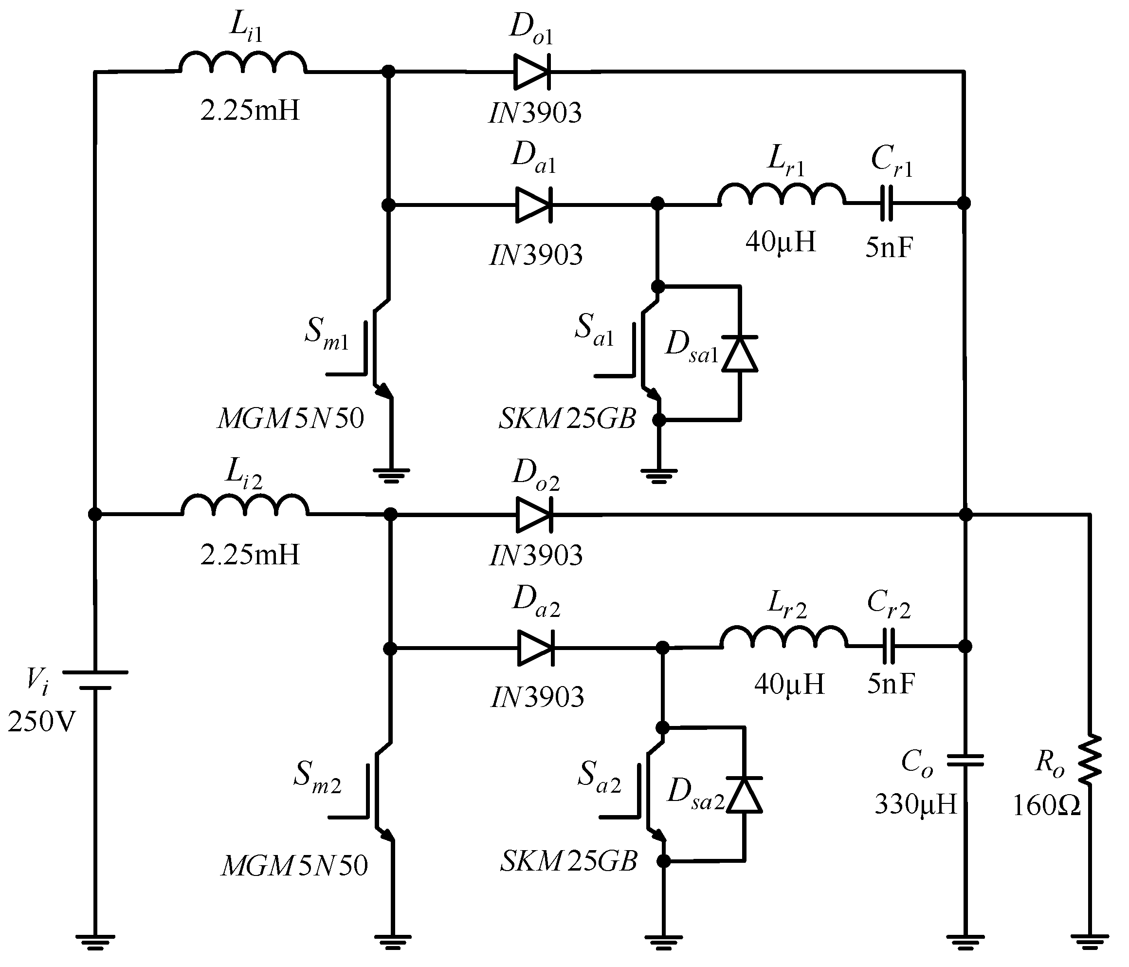
2. Proposed Converter

Figure 1 shows the proposed two-phase interleaved converter with a new zero current transition. Since this paper adopts the Interleaved PWM technique, the respective duty cycle of one phase differs by 180° from that of the other and does not overlap with each other. Accordingly, the operating principle of the single-phase circuit will be analyzed.
For analysis convenience of analyzing the proposed converter in each operating state, the following assumptions are made first: (i) The active power switch and the passive power switch are ideal; (ii) the input current is constant and the input inductance is much larger than the resonance inductance, which can be considered as a constant current source; (iii) the output voltage is fixed and the output capacitance is much larger than the resonant capacitance, so it can be regarded as a constant voltage source and (iv) Both the capacitance and inductance have no parasitic resistance.
From the above assumptions, the single-phase equivalent circuit will be shown in Figure 2.
Prior to the circuit analysis shown in Figure 2, the relevant component symbols are defined as follows: (i) Vo is the output DC voltage, vgm is the gate signal of the main switch Sm, vSm, is the voltage on the main switch, vga is the gate signal of the common-grounded auxiliary switch Sa, vSa is the voltage on the auxiliary switch, vDa is the voltage on the auxiliary diode Da, vDo is the voltage on the output diode Do, and vCr is the voltage on the resonant capacitor Cr and (ii) Iin is the DC current flowing through the input inductor, iSm is the current flowing through the main switch Sm, iSa is the current flowing through the auxiliary switch Sa, iDa is the current flowing through the auxiliary diode Da, iDo is the current flowing through the output diode Do, and iLr is the current flowing through the resonant inductor Lr. The internal diode Dsa is connected in parallel with Sa.
According to the on/off situation of the switching elements and the state of the energy storage elements, the main operating waveforms of the converter, shown in Figure 3, can be divided into seven over one switching cycle.
State 1 [ t 0 t t 1 ]: As shown in Figure 3 and Figure 4, when the time reaches t0, the main switch Sm is on and the rest of the switch elements are in the off state. At the same time, the input current Iin flows through Sm.
According to Figure 3, the following equations can be obtained as
{ i L r ( t ) = 0 v C r ( t ) = v C r ( t 0 )
The time experienced in this state, called Δt1, is
Δ t 1 = t 1 t 0 = D T s Δ t 2 Δ t 3 Δ t 4
where Δt2 is the time experienced in state 2, Δt3 is the time experienced in state 3, Δt4 is the time experienced in state 4, and D is the duty cycle.
State 2 [ t 1 t t 2 ]: As shown in Figure 3 and Figure 5, when the time reaches t1, the auxiliary switch Sa is turned on, and the output voltage Vo, resonant inductor Lr, and resonant capacitor Cr form a resonant circuit. At the same time, the resonant capacitor voltage vCr rises gradually from vCr(t0), and the resonant inductor current iLr starts to fall from zero. Once the voltage vCr rises to zero, the operating state proceeds to state 3.
The initial conditions of this state are
{ i L r ( t 1 ) = 0 v C r ( t 1 ) = v C r ( t 0 )
According to Figure 3, the following equations can be obtained as
{ i L r ( t ) = v C r ( t 0 ) V o Z r sin ω r ( t t 1 ) v C r ( t ) = V o + [ v C r ( t 0 ) V o ] cos ω r ( t t 1 )
The time experienced in this state, called Δt2, is
Δ t 2 = t 2 t 1 = 1 ω r sin 1 ( Z r I i n v C r ( t 0 ) V o )
State 3 [ t 2 t t 3 ]: As shown in Figure 3 and Figure 5, when the time reaches t2, the resonant inductor Lr and resonant capacitor Cr resonate continuously, and the resonant capacitor voltage vCr rises from zero, whereas the resonant inductor current iLr decreases continuously. When the resonant capacitor voltage vCr is equal to the output voltage Vo, the resonant inductor current iLr climbs upward from the reverse peak current. Once the resonant inductor current iLr climbs to zero, the operating state enters state 4.
The initial conditions of this state are
{ i L r ( t 2 ) = I i n v C r ( t 2 ) = 0
According to Figure 3, the following equations can be obtained to be
{ i L r ( t ) = I i n cos ω r ( t t 2 ) V o Z r sin ω r ( t t 2 ) v C r ( t ) = V o V o cos ω r ( t t 2 ) + Z r I i n sin ω r ( t t 2 )
The time experienced in this state, called Δt3, is
Δ t 3 = t 3 t 2 = 1 ω r cos 1 ( v C r ( t 0 ) V o V o 2 V o 2 + I i n 2 Z r 2 )
State 4 [ t 3 t t 4 ]: As shown in Figure 3 and Figure 6, when the time reaches t3, the auxiliary switch is cut off, and the resonant inductance Lr and resonant capacitance Cr continue to resonate, making the auxiliary diode conductive. At the same time, the resonant inductance current iLr starts to rise. According to Kirchhoff’s current law, it can be known that Ι i n = i S m + i L r . As the resonant inductance current iLr rises to the input current Iin, the main switch current iSm drops to zero. At this time, if the main switch is turned off, the ZCT of the main switch can be realized, and this state ends.
The initial conditions of this state are
{ i L r ( t 3 ) = 0 v C r ( t 3 ) = 2 V o v C r ( t 0 )
According to Figure 3, the following equations can be obtained as
{ i L r ( t ) = V o v C r ( t 0 ) Z r sin ω r ( t t 3 ) v C r ( t ) = V o + [ V o v C r ( t 0 ) ] cos ω r ( t t 3 )
The time experienced in this state, called Δt4, is
Δ t 4 = t 4 t 3 = 1 ω r sin 1 ( Z r I i n V o v C r ( t 0 ) )
State 5 [ t 4 t t 5 ]: As shown in Figure 3 and Figure 7, when the time reaches t4, the main switch Sm is cut off. At the same time, the resonant inductance Lr and resonant capacitance Cr continue to resonate. According to Kirchhoff’s current law, it can be known that Ι i n = i D a = i S a + i L r . Since the resonant inductance current iLr is greater than the input current In, the internal diode of the auxiliary switch, called DSa, is conductive. The moment the resonant inductance current iLr drops to the input current Iin, the operating state enters state 6.
The initial conditions of this state are
{ i L r ( t 4 ) = I i n v C r ( t 4 ) = V o + V o cos ( ω r Δ t 4 )
According to Figure 3, the following equations can be obtained as
{ i L r ( t ) = V o cos ( ω r Δ t 4 ) Z r sin ω r ( t t 4 )   + I i n cos ω r ( t t 4 ) v C r ( t ) = V o + [ V o cos ( ω r Δ t 4 ) ] cos ω r ( t t 4 )   Z r I i n sin ω r ( t t 4 )
The time experienced in this state, called Δt5, is
Δ t 5 = t 5 t 4 = 1 ω r sin 1 ( [ V o + V o cos ( ω r Δ t 4 ) ] I i n Z r [ V o cos ( ω r Δ t 4 ) ] 2 + I i n 2 Z r 2 )
State 6 [ t 5 t t 6 ]: As shown in Figure 3 and Figure 8, when the time reaches t5, the resonant inductor Lr and resonant capacitor Cr resonate continuously, thus causing the resonant inductor current iLr to drop from the input current In. According to Kirchhoff’s current law, it can be known that I i n = i D o + i L r . The resonant inductor current iLr is smaller than the input current In, thereby making the internal diode of the auxiliary switch, called DSa, cut off and the output diode Do conductive. As soon as the resonant inductor current iLr drops to zero, the operating state enters state 7.
The initial conditions of this state are
{ i L r ( t 5 ) = I i n v C r ( t 5 ) = 0
According to Figure 3, the following equations can be obtained as
{ i L r ( t ) = I i n cos ω r ( t t 5 ) v C r ( t ) = Z r I i n sin ω r ( t t 5 )
The time experienced in this state, called Δt6, is
Δ t 6 = t 6 t 5 = 1 ω r sin 1 ( v C r ( t 0 ) Z r I i n )
State 7 [ t 6 t t 7 ]: As shown in Figure 3 and Figure 9, when the time reaches t6, the resonance of resonant inductor Lr and resonant capacitor Cr is over; the resonant inductor current iLr has dropped to zero, so the auxiliary diode Da is cut off, which is like the demagnetization state of the input inductor of the traditional boost converter.
According to Figure 3, the following equations can be obtained as
{ i L r ( t ) = 0 v C r ( t ) = v C r ( t 0 )
The time experienced in this state, called Δt6, is
Δ t 7 = t 7 t 6 = ( 1 D ) T s Δ t 5 Δ t 6

3. Proposed Current Sharing Strategy

Since the proposed system uses the interleaved PWM technique, the two phases have a 180° difference in their individual gate driving signals and do not overlap their individual duty cycles with each other. Accordingly, a new current sampling method is adopted herein. In this paper, we use a new current sampling method to obtain two-phase current signals with only one current sampling circuit, which reduces one current sampling device, one filter circuit, and one analog-to-digital converter (ADC). Figure 10 shows the proposed two-phase current sampling method, where the sampling device for the two-phase current, the main switch current of the first phase, and the main switch current of the second phase are shown. In this system, a current sampling resistor Rc is connected in series with the emitters of the main switches of two phases. Based on the digital controller, the first-phase current is sampled from t0 to t1 time, and the second-phase current is sampled from t2 to t3 times so that the information of the two-phase current signals can be obtained.

3.1. Design of Current Sensing Resistor Rc

Prior to this section, the system specifications will be given as shown in Table 1.

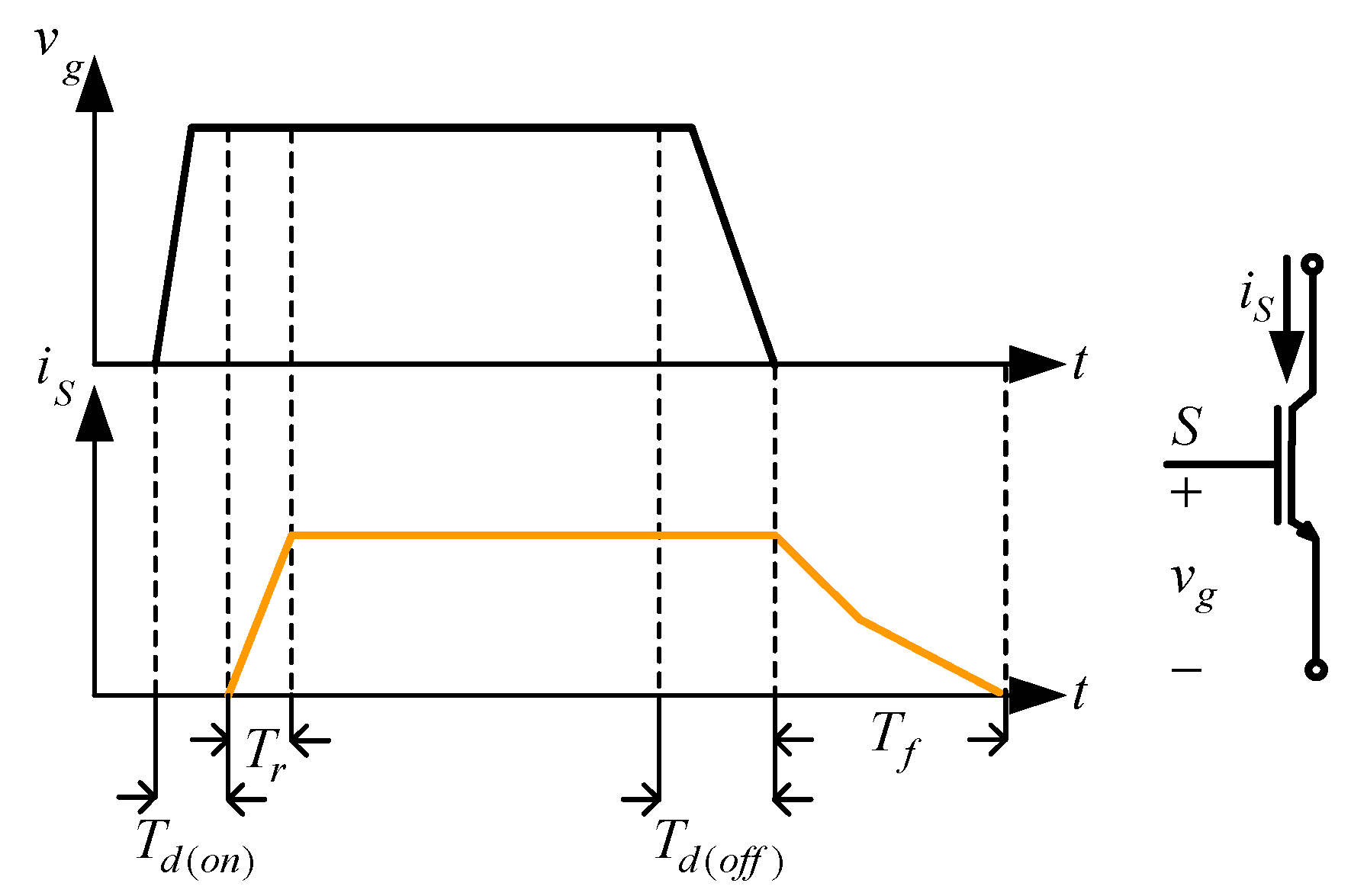
3.1.1. Maximum Input Inductor Current

Since this converter operates in CCM from light load to rated load, the corresponding duty cycle D is shown as below:
D = 1 V i V o = 1 250 400   =   0.375
The input inductor current ripple ΔiLi1 can be obtained as follows:
Δ i L i 1 = V i D T s L i 1 = 250 × 0.375 × 20 μ 1.66 m 1.13 A
The maximum input inductor current IL1,max can be obtained as follows:
I L i 1 , m a x = I L i 1 + 1 2 Δ i L i 1 = 2 + 1 2 × 1.13 2.57 A

3.1.2. Current Sensing Resistance

Figure 10a shows the isolated gate driver TLP-250 connected between gate G after resistor R2 and emitter E of the IGBT, whereas Figure 10b shows the current sensing resistor Rc for the two phases. From these two figures, it is noted that since the low-level output voltage of the gate driver is connected to point E, the current in the gate driver does not flow through Rc, which will guarantee that the IGBT works in the saturation region with VCE(sat) smaller than 2.5 V, which is verified by experiment. The following will talk about how to obtain the value of Rc.
Since the used current sensing resistor Rc has the loss, this loss due to Rc is set at 0.04% of the rated output power, that is, the power dissipated on Rc is 400 mW. The current, due to the gate driver, does not flow through Rc because the low-level output voltage of the gate driver is connected to point E.
According to Figure 10b, the rms value of the current flowing through Rc is
I c , r m s = 1 0.5 T s 0 D T s i S m 1 2 d t =   2 ( I L i 1 , m a x 2 2 I L i 1 , m a x Δ i L i 1 + Δ i L i 1 2 ) D + 2 3 Δ i L i 1 2 D = 3.935 A
Based on (23), two 0.1 Ω resistors connected in parallel are used as the current sensing resistor, where each resistor has a power dissipation of 200 mW, corresponding to the prescribed power dissipation. Since the maximum current flowing through Rc is equal to IL1,max, the maximum voltage on Rc is 0.1285 V. In addition, the maximum input voltage of the ADC is 5 V. Therefore, the voltage gain of the differential amplifier is set at 20, and hence, the ratio of voltage to current is 1 V/1 A and the maximum voltage on Rc is 2.57 V, corresponding to the ADC requirement.

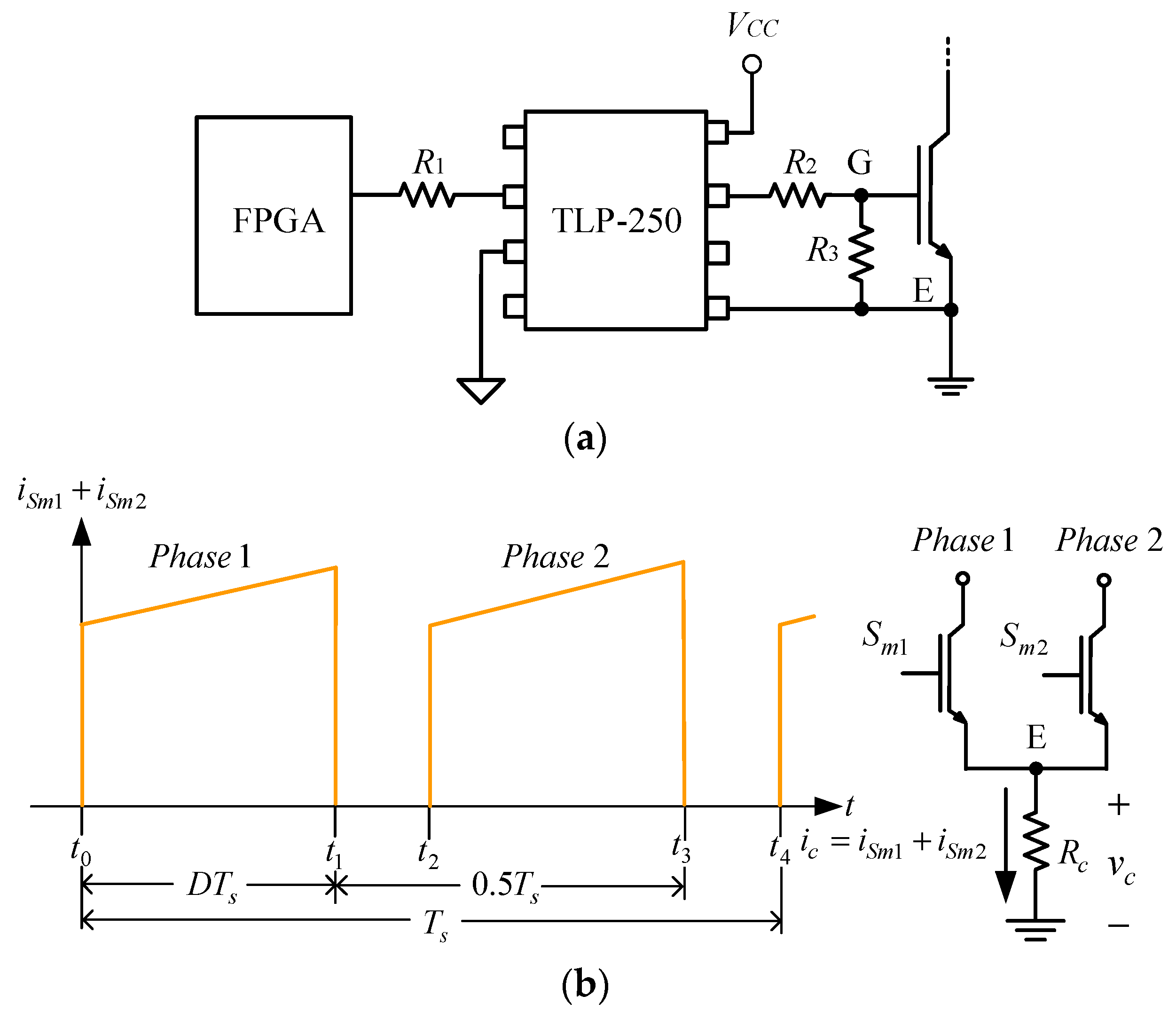
3.1.3. Current Sharing Controller

In this paper, the average current method is used to make the input current evenly distributed between the two phases, as shown in Figure 11. For the average current method to be considered, the sampled current signals of two phases are averaged to generate the current sharing reference command Iref. Sequentially, each phase current is subtracted from this reference command to generate the current error signal and then feeds this error signal to the corresponding current sharing compensator to obtain the required control force. After this, this control force is added with the voltage control force created from the voltage compensator to control the corresponding switch of each phase, so that current sharing, as well as output voltage stabilization, can be achieved.

4. Design of Resonant Components

This section introduces the resonant component design according to the given system specifications, the resonant inductors and resonant capacitors of two phases are designed. The system specifications are shown in Table 1. First, the on-time of the auxiliary switch should be given, and after this, the values of the resonant components will be calculated under the rated condition as the worst condition. Accordingly, the ZCT operation under the light condition can be guaranteed, and this can be verified by measured waveforms, to be seen later.
From Sec. 2, the turn-on time of the auxiliary switch is used to determine the resonance time. If the auxiliary switch conduction time is too long, it is easy to cause an excessive increase in conduction loss, whereas if the turn-on time of the auxiliary switch is less than the sum of the cut-off delay time Td(off) and falling time Tf of the IGBT, the resonance inductor Lr and the resonance capacitor Cr will resonate several times and affect the operation of the auxiliary circuit. According to Figure 12, the on-time of the auxiliary switch must be greater than the sum of Td(off) and Tf. Therefore, to reduce the effect of the resonance frequency on PWM switching, the resonance period is set between 0.05 times the switching period and 0.1 times the switching period, that is, the resonance period locates between 1 μs and 2 μs, so the turn-on time of the auxiliary switch is taken as 1.5 μs.
According to Figure 3, since the resonant inductor and resonant capacitor resonate with two times the turn-on time of the auxiliary switch, the resonant angular frequency can be obtained to be
ω r = 2 π × f r = 2 π × 1 2 × 1.5 μ   = 2.1 M rad / s
To ensure that the main switch can reach turn-off ZCT from light load to rated load, the peak current of the resonant inductor must be larger than the peak current of the input inductor, and when one phase is broken, the other phase must continue to operate. Therefore, the peak current of the resonant inductor is twice the peak current of the input inductor, and the resonant impedance can be obtained as
2 I L i 1 , m a x = V o v C r ( t 0 ) Z r Z r = V o v C r ( t 0 ) 2 I L i 1 , m a x
As shown in Figure 3, the following equation can be approximately obtained to be
v C r ( t 0 ) Z r I L i 1 , m a x = Z r I L i 1 , m a x v C r ( t 0 ) V o
Substituting (22) and (25) into (26) yields the initial resonant capacitance across the voltage as
v C r ( t 0 ) = 6 V o 36 V o 2 + 12 V o 2 6 = 62 V
By substituting (25) into (26) and (27), the values of the resonant inductor and resonant capacitor can be obtained to be
{ L r = Z r ω r 40 μ H C r = 1 ω r Z r 5 nF
As shown in Figure 3, the maximum voltage across the resonant capacitor is 2Vo-vCr(t0), i.e., 862 V. Therefore, the resonant capacitor takes a 1.5 kV Mylar capacitor, and the resonant inductor adopts a Sendust core manufactured by CHANGSUNG, with the model number CS270125, 18 turns, and the wire diameter No. 16 AWG.

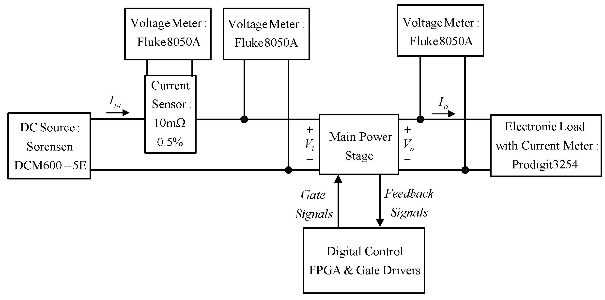
5. System Configuration

In Figure 13, the main power stage is composed of a two-phase interleaved step-up converter with a ZCT auxiliary circuit, whereas the peripheral circuit includes a gate driver circuit, a voltage sampling circuit, a two-phase current sampling circuit and an analog-to-digital converter; in the controller, the FPGA is used as the control kernel to realize the fully digital interleaved PWM control. The Cyclone II series FPGA chip, manufactured by Altera Co., has a product number of EP2C20F484C8.

6. Simulated and Experimental Results and Discussions

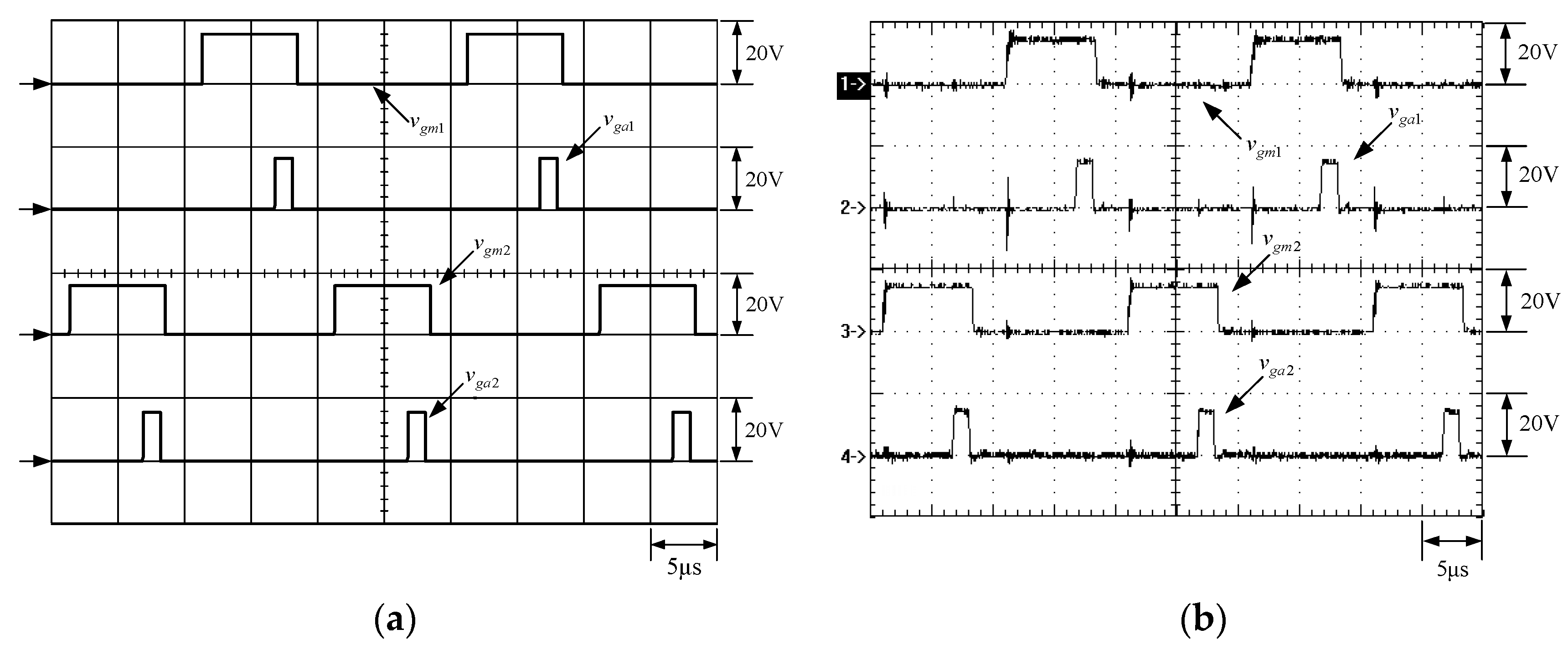
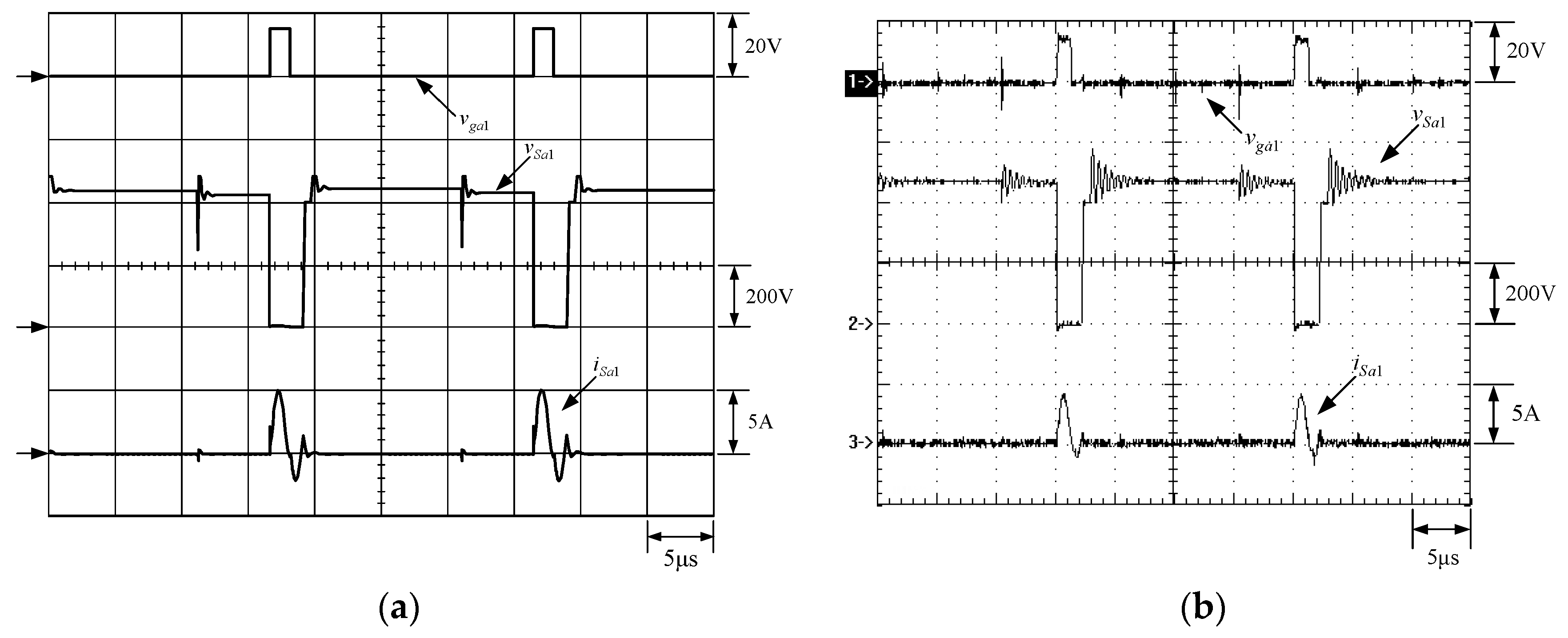
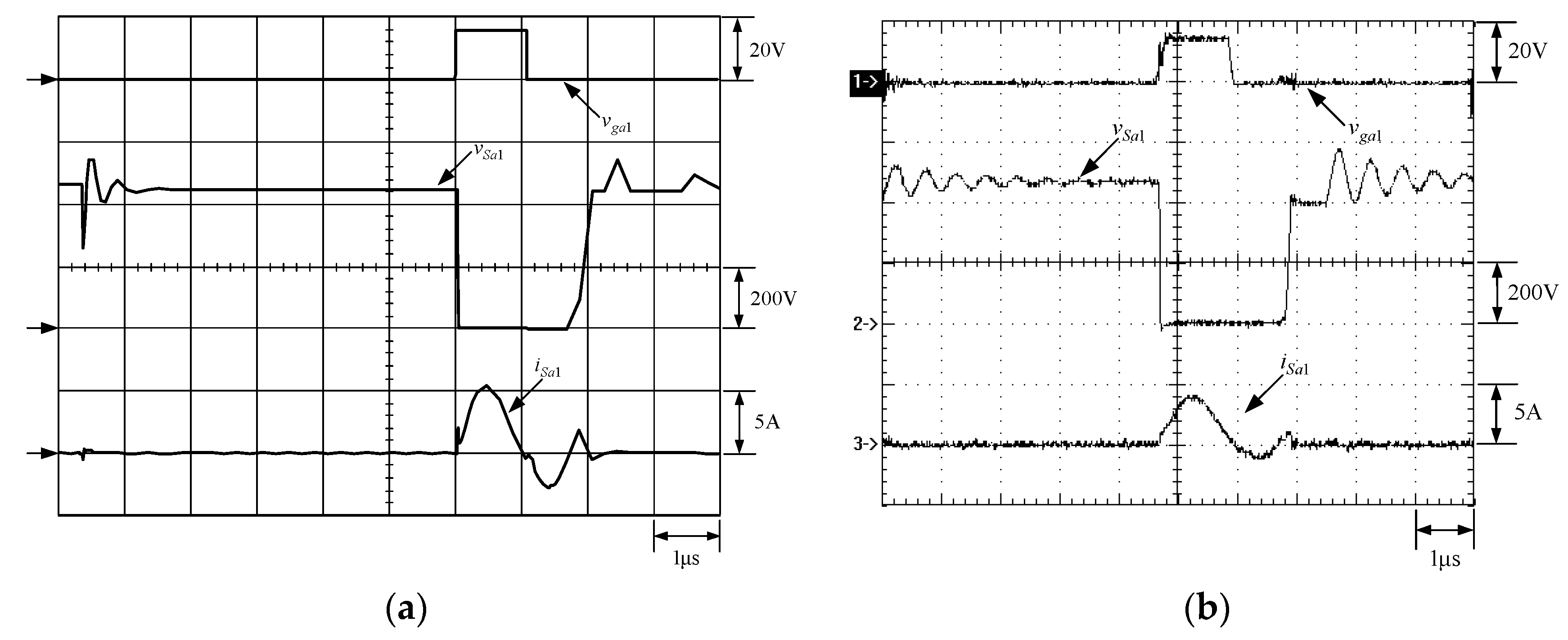
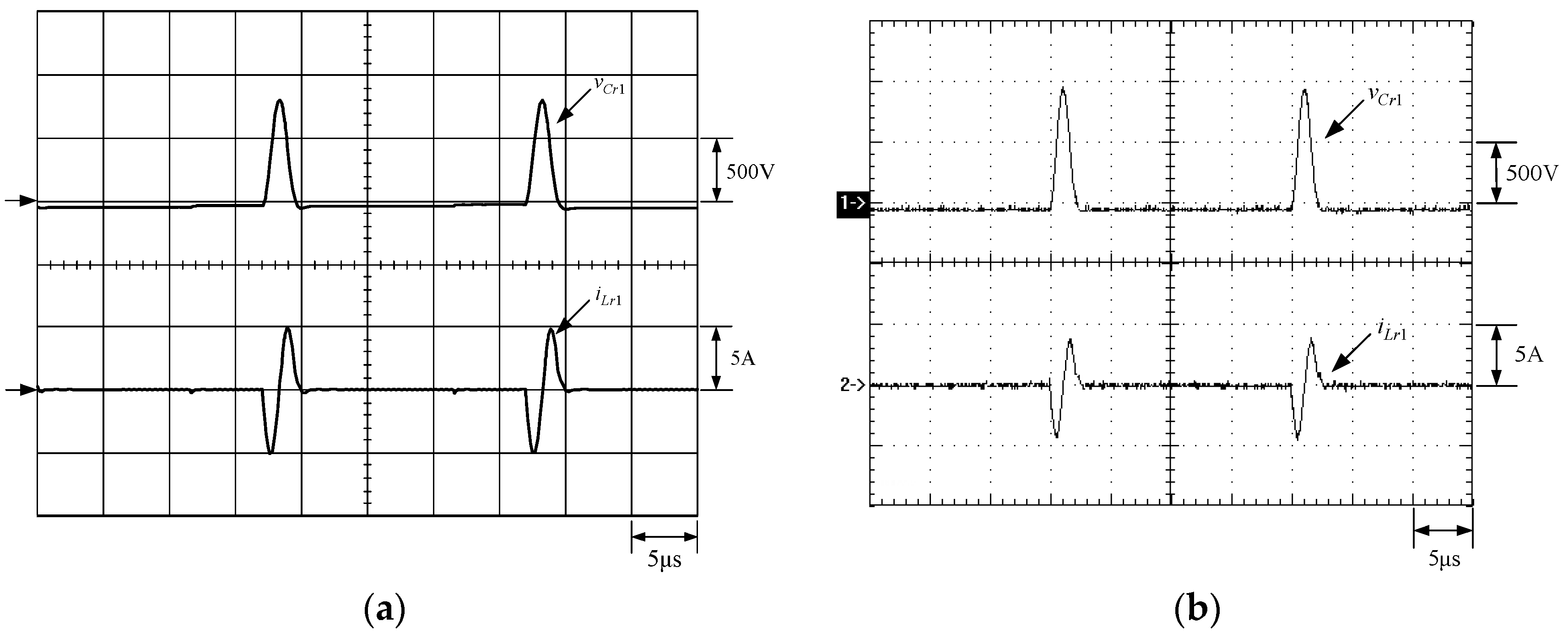
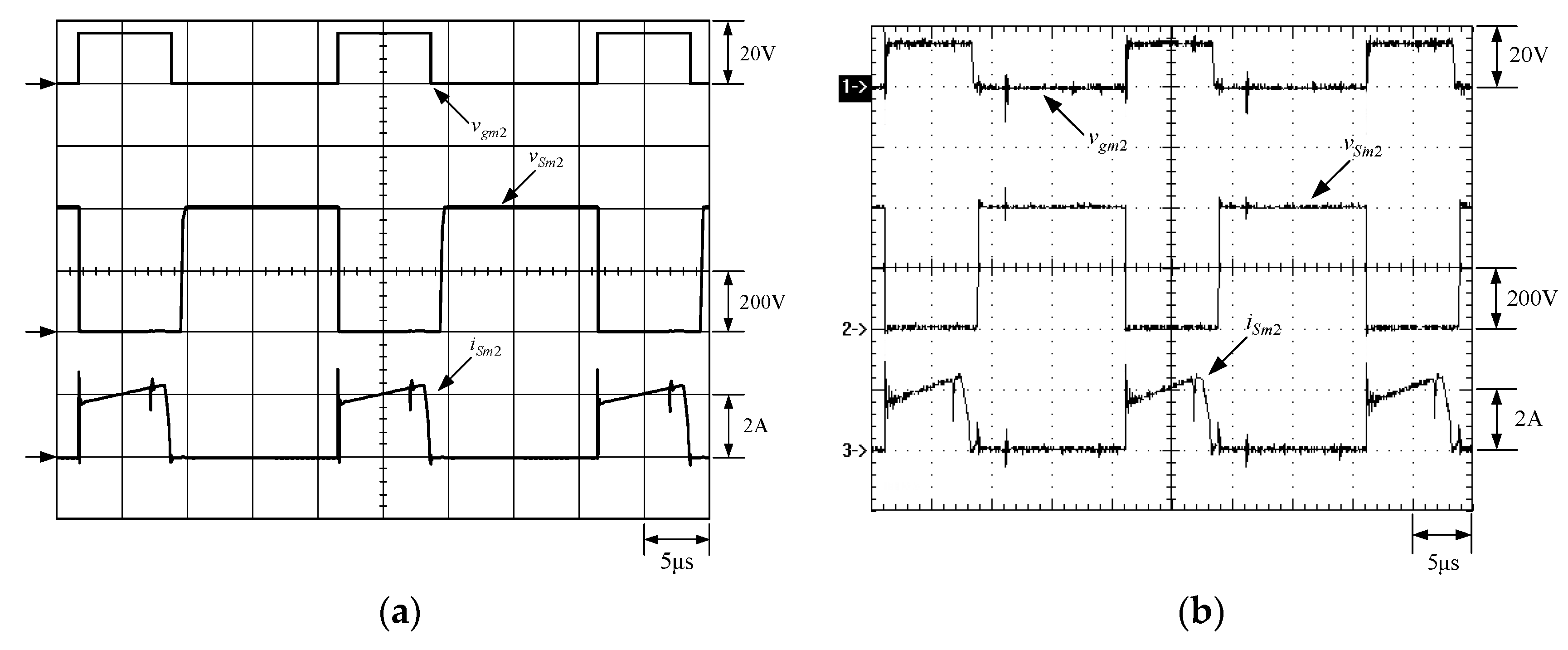
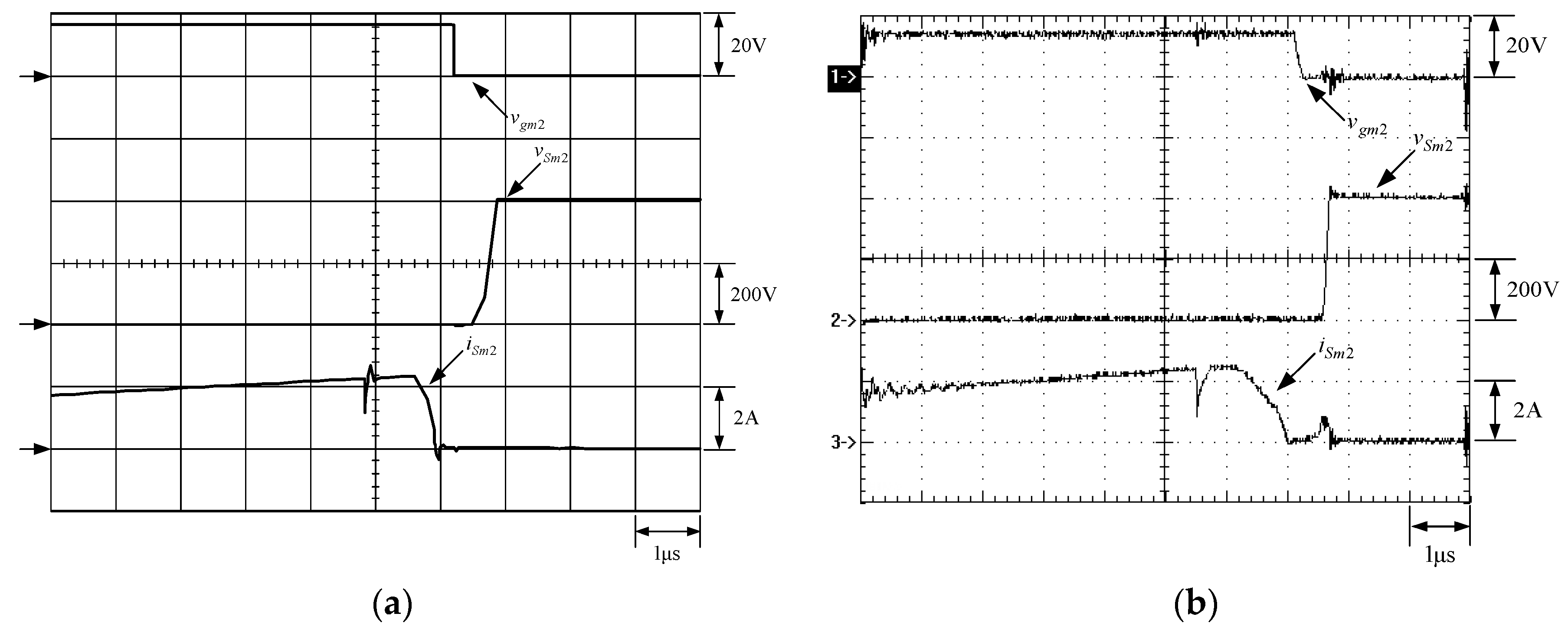
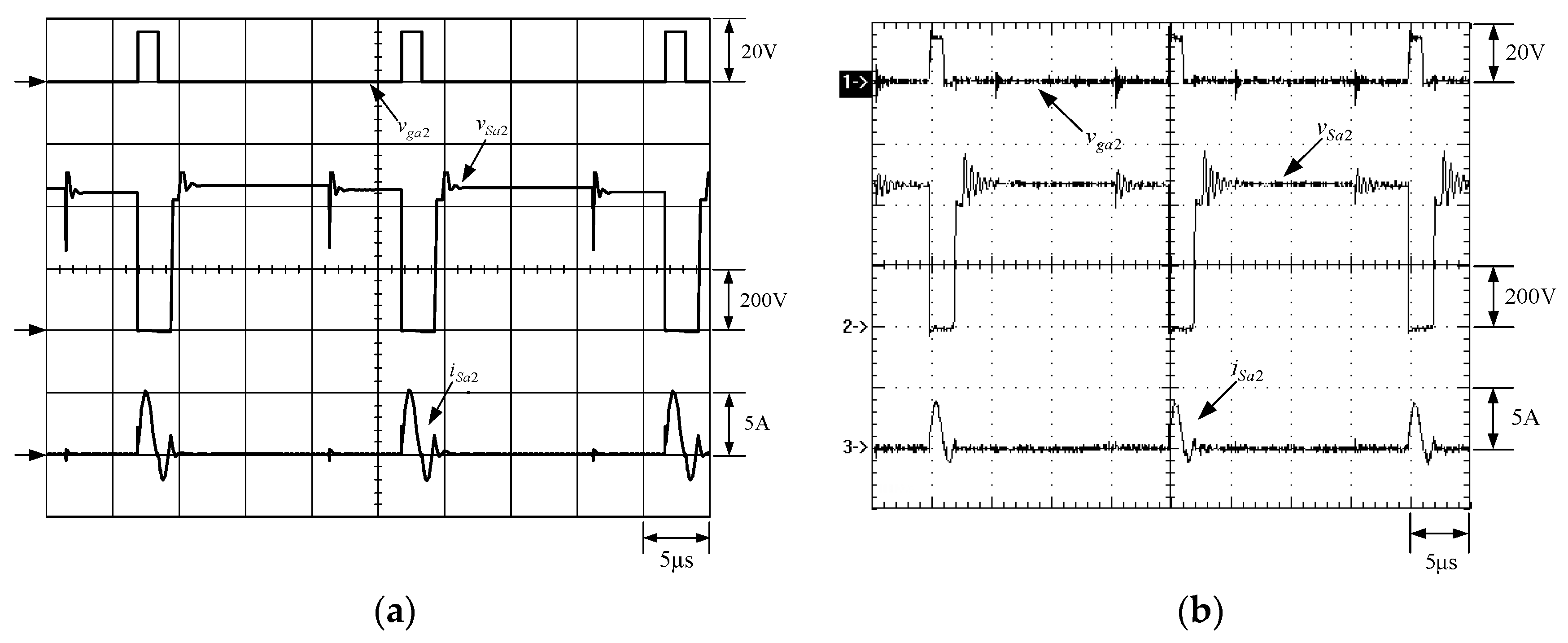
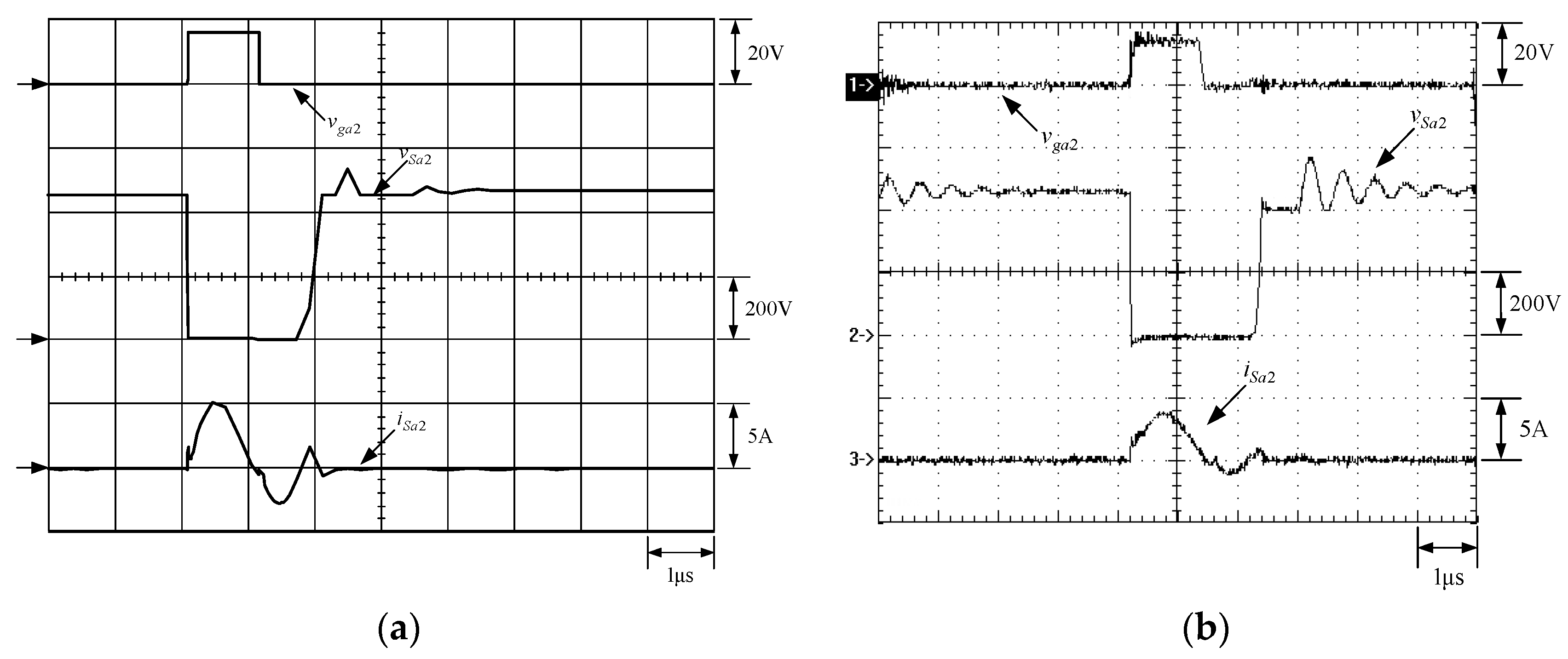
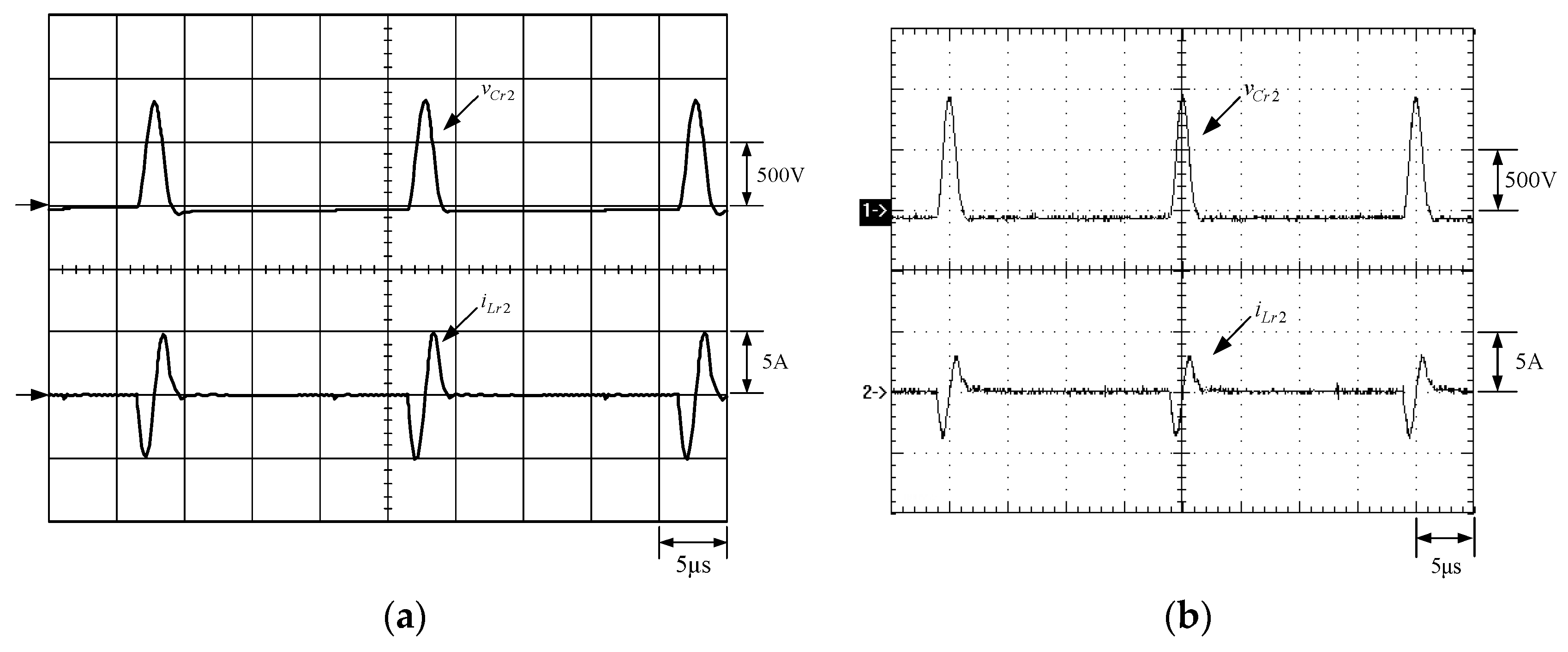
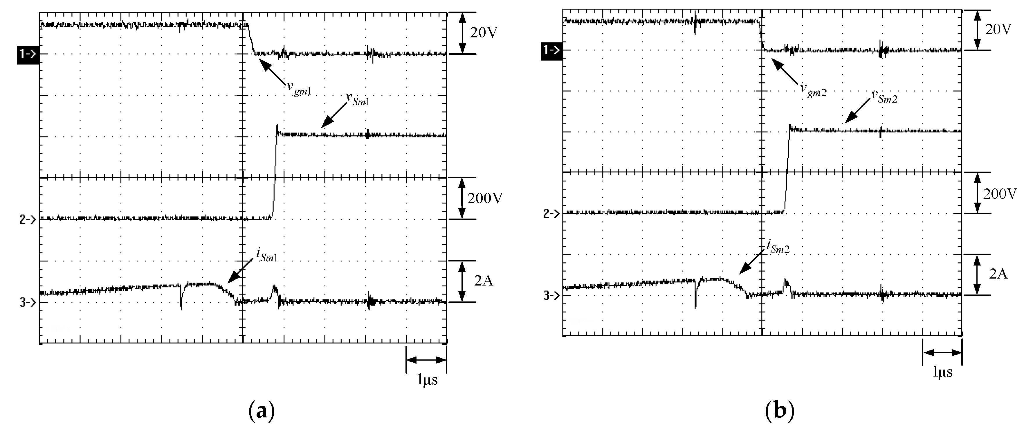
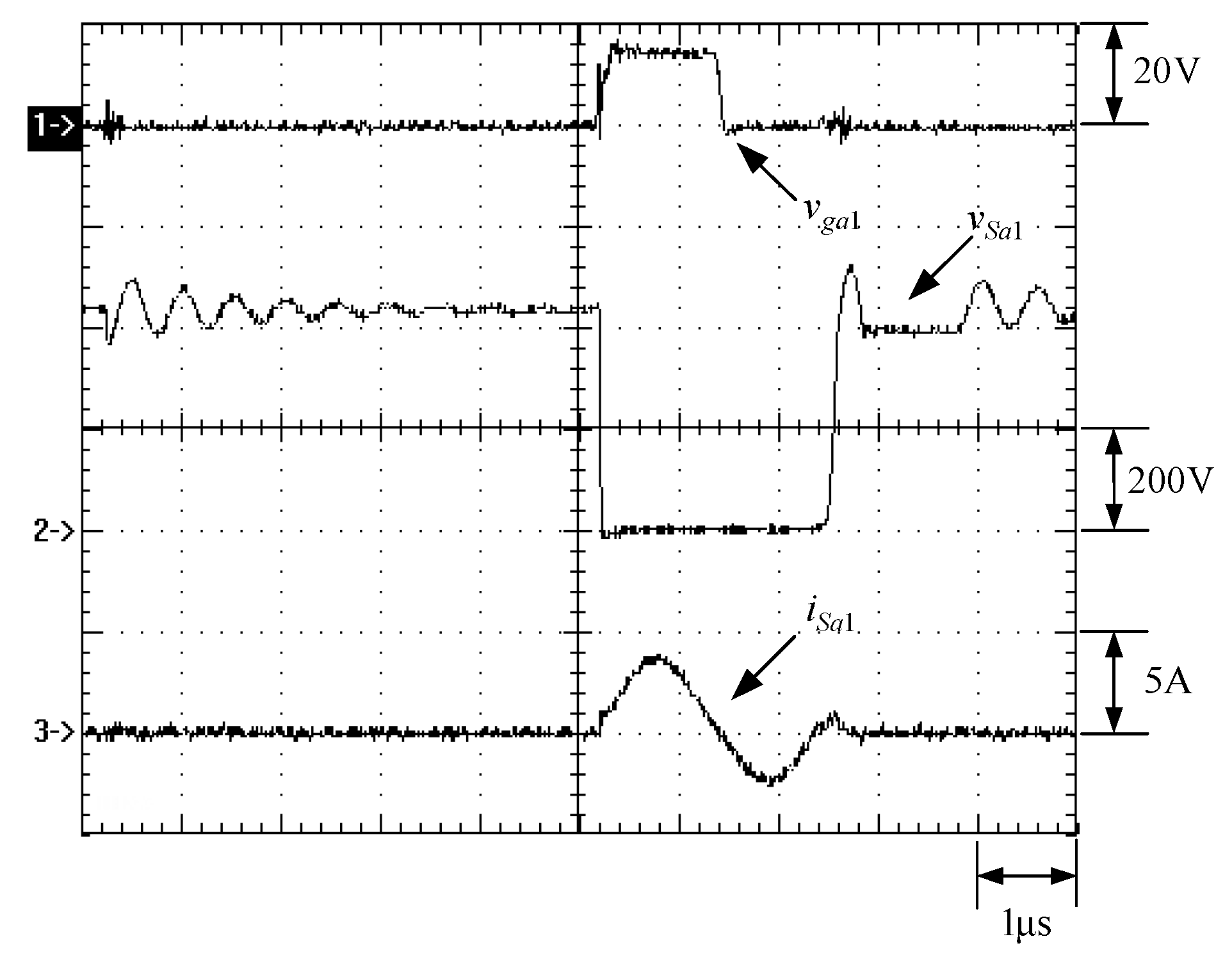
6.1. Simulated and Measured Waveforms

The simulation shown in Figure 14 is based on the IsSpice software. In the following, the simulated and experimental results are obtained at rated load. Moreover, in Table 2, the part numbers used for the switches and diodes in the simulation and experiment can be configured according to the system specifications and the main operating waveforms.
Figure 15 shows the gate driving signals for main switches vgm1 and vgm2, and auxiliary switches vga1 and vga2. Figure 16 shows the gate driving signal for the phase-1 main switch Sm1, called vgm1, the voltage across Sm1, called vSm1, and the current flowing through Sm1, called iSm1. Figure 17 shows the zoom-in of Figure 16. Figure 18 shows the gate driving signal for the phase-1 auxiliary switch Sa1, called vga1, the voltage across Sa1, called vSa1, and the current flowing through Sa1, called iSa1. Figure 19 shows the zoom-in of Figure 18. Figure 20 shows the voltage on the resonant capacitor, called vCr1, and the current flowing through the resonant inductor, called iLr1.
Figure 21 shows the gate driving signal for the phase-2 main switch Sm2, called vgm2, the voltage across Sm2, called vSm2, and the current flowing through Sm2, called iSm2. Figure 22 shows the zoom-in of Figure 21. Figure 23 shows the gate driving signal for the phase-2 auxiliary switch Sa2, called vSa2, called vga2, the voltage across Sa2, called vSa2, and the current flowing through Sa2, called iSa2. Figure 24 shows the zoom-in of Figure 23. Figure 25 shows the voltage on the resonant capacitor, called vCr2, and the current flowing through the resonant inductor, called iLr2. Figure 26 shows the gate driving signals vgm1 and vgm2, and the resonant inductor currents iLr1 and iLr2.

6.2. Waveform Comments

The simulated and experimental results are similar to some extent except for oscillation. From Figure 15, vgm2 is shifted by 180 degrees from vgm1 whereas vga2 is shifted by 180 degrees from vga1. Figure 17 shows Sm1 has turn-off ZCT. Figure 19 shows vSa1 and iSa1, corresponding to near ZCS. Figure 20 shows vCr1 and iLr1, also corresponding to Figure 3. Figure 22 shows Sm2 has turn-off ZCT. Figure 24 shows vSa2 and iSa2, corresponding to near ZCS. Figure 25 shows vCr2 and iLr2, also corresponding to Figure 3. Figure 26 shows iL2 is shifted by 180 degrees from iL2, the average values of the two currents are almost the same, meaning that the output current is almost distributed between the two phases.
In Figure 16 or Figure 21, there are four phenomena to be described. One is the current spike in iSm1 or iSm2 is due to the reverse recovery current of Do1 or Do1, and the voltage vSm1 or vSm2 during the turn-on period is smaller than the maximum on-voltage drop VCE(sat) of 2.5 V based on the STGP10NC60H datasheet, thereby making sure that Sm1 or Sm2 are operated in the saturation region. Another is that iSm1 or iSm2 will have a small increase when the voltage across Sm1 or Sm2 rises since the IGBT needs time to withdraw injected carriers at the emitter of the IGBT during the turn-off period. The other is that as Sa1 or Sa2 is on instantaneously, the corresponding Da1 or Da2 is on, so some of the currents in Sm1 or Sm2 will be shifted to Sa1 or Sa2, resulting in a current dip in current iSm1 or iSm2.
In Figure 18 or Figure 23, there are two ringing voltages on vSa1 or vSa2 to be described. One is that since the reverse recovery current of DSa1 or DSa2 will flow to the resonant path, the first ringing voltage on vSa1 or vSa2 will occur. The other is that when Sm1 or Sm2 turn on instantaneously, the reverse recovery current of Do1 or Do2 will flow to the resonant path through Da1 or Da2, so the second ringing voltage on vSa1 or vSa2 will occur.
In Figure 20 or Figure 25, the peak value of the resonant inductor current is smaller than the designed value due to the presence of parasitic resistance in the actual circuit, and the peak value of the resonant capacitor voltage is larger than the designed value due to the tolerance of the resonant capacitance. From Figure 27, it is noted that at light load, the main switches Sm1 and Sm2 still have ZCT turn-off, corresponding to the requirements.

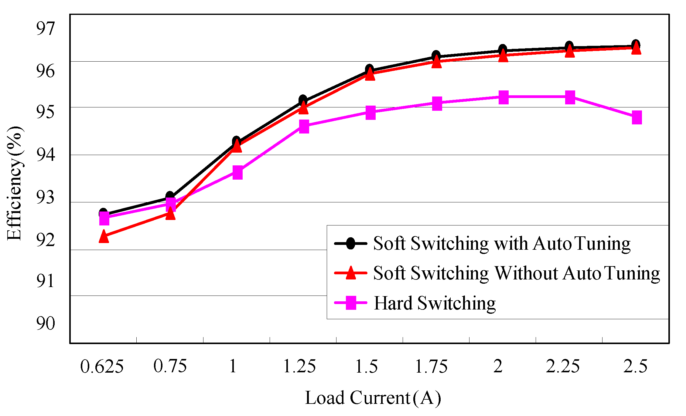
6.3. Light-Load Efficiency Improvement

Figure 28 shows the waveforms of Sa1 under 25% load by not adjusting the on-time and off-triggering moment of Sa1. As can be seen from this figure, when the proposed converter is operated under a light load, the current flowing through Dsa1 is larger than that under a rated load. Therefore, the reverse recovery current of this diode is larger than that under a rated load, so a voltage spike on Sa1 is likely to be caused. Figure 29 shows the waveforms of Sa1 under 25% load by adjusting the on-time and off-triggering moment of Sa1. The peak value of the voltage spike will be reduced from 620 V to 460 V, thereby making the light-load efficiency improved. This description can be applied to phase-2 Sa2.

6.4. Efficiency Measurement

Figure 30 shows the efficiency measurement block diagram. From this figure, a current sampling resistor is connected in series with the input current path. The input current and input voltage are multiplied to obtain the input power. To measure the output power, an electronic load, named Prodigit 3254, is used to provide the required load current, and a digital voltmeter, named Fluke 8050 A, is used to measure the output voltage, which is multiplied by the load current to obtain the output power. Eventually, the output power at each load is divided by the corresponding input power to obtain a curve of efficiency versus load current shown in Figure 31. In Figure 31, there are three cases to be compared. Case 1 has the ZVT turn-on without the on-time and the off-triggering instant of Sa1 and Sa2 adjusted. Case 2 has the ZVT turn-on with the on-time and the off-triggering instant of Sa1 and Sa2 adjusted. Case 3 has no ZVT. From this figure, Case 2 has better light-load efficiency than the other two. The rated load efficiencies for Case 1, Case 2 and Case 3 are 96.3%, 96.4% and 94.8%, respectively. Since the power loss relevant to the tail current is quite difficult to estimate [24], we use the rated-load efficiencies for Case 3 and Case 1 to figure out the individual power losses of 54.8 W and 38.4 W, respectively, and then the power loss associated to the falling current can be approximately estimated out by the difference in power loss between these two cases, equal to 16.4 W.

6.5. Comparison between the Existing and the Proposed

In Table 3, the literature [14] has the least number of main switches, and the main switches have a hard turn-on and ZCS turn-off; however, the main switches will have large current stresses when they are turned off. In [9], the main switches have a large voltage spike when they are turned off. Additionally, although the auxiliary switches have turn-off ZVS and ZCS, they are turned off with higher voltage surges so that the components with higher voltage withstand are needed. The output diode, although it has a turn-on near ZCS and turn-off ZVZCS in [9], there are high resonance voltages and resonance currents, resulting in the need for a higher voltage and current-withstanding components for the output diode. The auxiliary diode has a soft switching function in every literature except for [14]. The maximum efficiency is the highest in [13]; however, the average efficiency of [13] is not the highest. Although the maximum efficiency of the proposed circuit is not the highest, its average efficiency has been improved by using an auto-tuning technique, and hence the practicality of this circuit has been greatly increased.

7. Conclusions

This paper proposes a fully digital multiphase interleaved boost converter with a fixed-frequency ZCT. The proposed auxiliary circuits used to realize the ZCT with the common-grounded auxiliary switches are added to the traditional boost converter to reduce the switching loss caused by the hard switching of IGBTs. In addition, the overall efficiency of the converter can be improved by adjusting the on-time and off-trigger times of the auxiliary switch. Furthermore, a current-sharing control along with a two-phase interleaved control is used to distribute the input current evenly among the phases. In addition, a new current sampling method is used, which requires only one sampling circuit to simultaneously return the current signals of the two-phase main switches. Above all, the number of phases can be extended, still possessing easy control of the ZCT and current sharing.

Author Contributions

Conceptualization, K.-I.H. and P.-C.T.; methodology, K.-I.H. and P.-C.T.; software, P.-C.T.; validation, K.-I.H. and P.-C.T.; formal analysis, P.-C.T.; investigation, P.-C.T.; resources, P.-C.T.; data curation, P.-C.T.; writing—original draft preparation, K.-I.H.; writing—review and editing, K.-I.H.; visualization, P.-C.T.; supervision, K.-I.H.; project administration, K.-I.H.; funding acquisition, K.-I.H. All authors have read and agreed to the published version of the manuscript.

Funding

This research was funded by the Ministry of Science and Technology, Taiwan, under Grant Number: MOST 110-2221-E-027-045-MY2.

Data Availability Statement

No new data were created or analyzed in this study. Data sharing is not applicable to this article.

Conflicts of Interest

The authors declare no conflict of interest.

References

  1. Erickson, R.W.; Maksimovic, D. Fundamental Power Electronics, 2nd ed.; Electronic Services: Boulder, CO, USA, 2001. [Google Scholar]
  2. Liu, K.; Lee, F.C. Resonant switches: A unified approach to improving performances of switching converters. In Proceedings of the INTELEC’84-International Telecommunications Energy Conference, New Orleans, LA, USA, 4–7 November 1984; pp. 344–359. [Google Scholar]
  3. Lee, F.C. High-frequency quasi-resonant and multi-resonant converter technologies. In Proceedings of the 14 Annual Conference of Industrial Electronics Society, Singapore, 24–28 October 1988; pp. 509–521. [Google Scholar]
  4. Tutakne, D.R.; Suryawanshi, H.M.; Tarnekar, S.G. Universal input zero current switched high power factor variable speed DC drive. IEEE Trans. Ind. Electron. 2006, 12, 1618–1623. [Google Scholar]
  5. Martins, M.L.S.; Hey, H.L. Self-commutated auxiliary circuit ZVT PWM converters. IEEE Trans. Power Electron. 2004, 19, 1435–1445. [Google Scholar] [CrossRef]
  6. Choi, H.S.; Cho, B.H. Zero current switching (ZCS) power factor pre-regulator (PFP) with reduced conduction losses. In Proceedings of the Eighteenth Annual IEEE Applied Power Electronics Conference and Exposition, Dalla, TX, USA, 10–14 March 2002; pp. 962–967. [Google Scholar]
  7. Qin, L.; Shaojun, X.; Zhou, H. A novel family of PWM converters based on improved ZCS switch cell. In Proceedings of the 2007 IEEE Power Electronics Specialists Conference, Orlando, FL, USA, 17–21 June 2007; pp. 2725–2730. [Google Scholar]
  8. Ling, Q.; Yafang, W.; Juping, G.; Huiling, X. A novel family of ZCS-PWM converters minimizing additional conduction loss. In Proceedings of the 2008 International Conference on Electrical Machines and Systems, Wuhan, China, 17–20 October 2008; pp. 1716–1720. [Google Scholar]
  9. Wang, C.M. A new family of zero-current-switching (ZCS) PWM converters. IEEE Trans. Ind. Electron. 2005, 52, 1117–1125. [Google Scholar] [CrossRef]
  10. Mao, H.; Lee, F.C.; Zhou, X.; Boroyevich, D. Improved zero-current transition converters for high power applications. In Proceedings of the Conference Record of the 1996 IEEE Industry Applications Conference Thirty-First IAS Annual Meeting, San Diego, CA, USA, 6–10 October 1996; pp. 1145–1152. [Google Scholar]
  11. Bodur, H.; Bakan, A.F. An improved ZCT-PWM DC-DC converter for high-power and frequency applications. IEEE Trans. Ind. Electron. 2004, 51, 89–95. [Google Scholar] [CrossRef]
  12. Saravanan, K.K.; Rajalakshmi, S.; Stalin, N.; Titus, S. New zero current transition PWM dc/dc converter without current stress. In Proceedings of the 2012 International Conference on Advances in Engineering, Science and Management (ICAESM 2012), Nagapattinam, India, 30–31 March 2012; pp. 566–570. [Google Scholar]
  13. Mao, H.; Lee, F.C.; Zhou, X.; Dai, H.; Cosan, M.; Boroyevich, D. Improved zero-current transition converters for high-power applications. IEEE Trans. Ind. Appl. 1997, 33, 1220–1232. [Google Scholar]
  14. Yazdani, M.R.; Farzanehfard, H.; Faiz, J. EMI Analysis and evaluation of an improved ZCT flyback converter. IEEE Trans. Power Electron. 2011, 26, 2326–2334. [Google Scholar] [CrossRef]
  15. Lee, D.-Y.; Lee, M.-K.; Hyun, D.-S.; Choy, I. New zero-current-transition PWM DC/DC converters without current stress. IEEE Trans. Power Electron. 2003, 18, 95–104. [Google Scholar]
  16. Das, P.; Moschopoulos, G. A comparative study of zero-current-transition PWM converters. IEEE Trans. Ind. Electron. 2007, 54, 1319–1328. [Google Scholar] [CrossRef]
  17. Wang, C.M. New family of zero-current-switching PWM converters using a new zero-current-switching PWM auxiliary circuit. IEEE Trans. Ind. Electron. 2006, 53, 768–777. [Google Scholar] [CrossRef]
  18. Yau, Y.T.; Hwu, K.I.; Shieh, J.J. Minimization of output voltage ripple of two-phase interleaved buck converter with active clamp. Energies 2021, 14, 5215. [Google Scholar] [CrossRef]
  19. Hwu, K.I.; Shieh, J.J.; Jiang, W.Z. Interleaved boost converter with ZVT-ZCT for main switches and ZCS for auxiliary switch. Appl. Sci. 2020, 10, 2033. [Google Scholar] [CrossRef] [Green Version]
  20. Yau, Y.T.; Hwu, K.I.; Jiang, W.Z. Two-phase interleaved boost converter with ZVT turn-on for main switches and ZCS turn-off for auxiliary switches based on one resonant loop. Appl. Sci. 2020, 10, 3881. [Google Scholar] [CrossRef]
  21. Guoyong, G.; Bingxue, S. Design of multi-phase DC-DC converter with master-slave current sharing control. In Proceedings of the 2002 IEEE Region 10 Conference on Computers, Communications, Control and Power Engineering, Beijing, China, 28–31 October 2002; pp. 1990–1993. [Google Scholar]
  22. Huang, W.; Schuellein, G.; Clavette, D. A scalable multiphase buck converter with average current share bus. In Proceedings of the Eighteenth Annual IEEE Applied Power Electronics Conference and Exposition, Miami Beach, FL, USA, 9–13 February 2003; pp. 438–443. [Google Scholar]
  23. Hwu, K.I.; Yau, Y.T. Applying one-comparator counter-based sampling to current sharing control of multichannel LED strings. IEEE Trans. Ind. Appl. 2011, 47, 2413–2421. [Google Scholar] [CrossRef]
  24. Baliga, B.J. Fundamental Power Semiconductor Devices, 1st ed.; Springer: New York, NY, USA, 2008. [Google Scholar]
Figure 1. Proposed converter.
Micromachines 13 02055 g001
Figure 2. Single-phase equivalent circuit.
Micromachines 13 02055 g002
Figure 3. Main operating waveforms.
Micromachines 13 02055 g003
Figure 4. Current flow of state 1.
Micromachines 13 02055 g004
Figure 5. Current flow of state 2.
Micromachines 13 02055 g005
Figure 6. Current flow of state 4.
Micromachines 13 02055 g006
Figure 7. Current flow of state 5.
Micromachines 13 02055 g007
Figure 8. Current flow of state 6.
Micromachines 13 02055 g008
Figure 9. Current flow of state 7.
Micromachines 13 02055 g009
Figure 10. Proposed sampling method: (a) Relationship between TLP250 and IGBT; (b) Relationship between two TLP250s and Rc.
Micromachines 13 02055 g010
Figure 11. Block diagrams of the average current method.
Micromachines 13 02055 g011
Figure 12. IGBT on delay time and off delay time.
Micromachines 13 02055 g012
Figure 13. System circuit configuration.
Micromachines 13 02055 g013
Figure 14. IsSpice simulation of the proposed circuit with selected component models and parameters.
Micromachines 13 02055 g014
Figure 15. Waveforms relevant to gate driving signals: (1) vgm1; (2) vga1; (3) vgm2; (4) vga2 for (a) simulation and (b) experiment.
Micromachines 13 02055 g015
Figure 16. Waveforms relevant to Sm1: (1) vgm1; (2) vSm1; (3) iSm1 for (a) simulation and (b) experiment.
Micromachines 13 02055 g016
Figure 17. Zoom-in of Figure 17: (1) vgm1; (2) vSm1; (3) iSm1 for (a) simulation and (b) experiment.
Micromachines 13 02055 g017
Figure 18. Waveforms relevant to Sa1: (1) vga1; (2) vSa1; (3) iSa1 for (a) simulation and (b) experiment.
Micromachines 13 02055 g018
Figure 19. Zoom-in of Figure 19: (1) vga1; (2) vSa1; (3) iSa1 for (a) simulation and (b) experiment.
Micromachines 13 02055 g019
Figure 20. Waveforms relevant to Cr1 and Lr1: (1) vCr1; (2) iLr1 for (a) simulation and (b) experiment.
Micromachines 13 02055 g020
Figure 21. Waveforms relevant to Sm2: (1) vgm2; (2) vSm2; (3) iSm2 for (a) simulation and (b) experiment.
Micromachines 13 02055 g021
Figure 22. Zoom-in of Figure 23: (1) vgm2; (2) vSm2; (3) iSm2 for (a) simulation and (b) experiment.
Micromachines 13 02055 g022
Figure 23. Waveforms relevant to Sa2: (1) vga2; (2) vSa2; (3) iSa2 for (a) simulation and (b) experiment.
Micromachines 13 02055 g023
Figure 24. Zoom-in: (1) vga2; (2) vSa2; (3) iSa2 for (a) simulation and (b) experiment.
Micromachines 13 02055 g024
Figure 25. Waveforms relevant to Cr2 and Lr2: (1) vCr2; (2) iLr2 for (a) simulation and (b) experiment.
Micromachines 13 02055 g025
Figure 26. Waveforms relevant to Li1 and Li2: (1) vgm1; (2) vgm2; (3) iLi2; (4) iLi2 for (a) simulation and (b) experiment.
Micromachines 13 02055 g026
Figure 27. Waveforms under 25% load: (1) vgm1; (2) vSm1; (3) iSm1 for (a) Sm1; (1) vgm2; (2) vSm2; (3) iSm2 for (b) Sm2.
Micromachines 13 02055 g027
Figure 28. Waveforms related to phase-1 Sa1 under 25% load without the on-time and off-triggering moment of Sa1 adjusted: (1) vga1; (2) vSa1; (3) iSa1.
Micromachines 13 02055 g028
Figure 29. Waveforms related to phase-1 Sa1 under 25% load with the on-time and off-triggering moment of Sa1 adjusted: (1) vga1; (2) vSa1; (3) iSa1.
Micromachines 13 02055 g029
Figure 30. Efficiency measurement block diagram.
Micromachines 13 02055 g030
Figure 31. Curves of efficiency versus load current.
Micromachines 13 02055 g031
Table 1. System specifications.
SpecificationValue or Condition
Input Voltage (Vi)250 V
Output Voltage (Vo)400 V
Rated Output Current (Io,rated)/Rated Output Power (Po,rated)2.5 A/1 kW
Min. Output Current (Io,min)/Min. Output Power (Po,min)0.625 A/0.25 kW
Switching Frequency (fs)/Switching Period (Ts)50 kHz/20 μs
Operating ModeContinuous Current Mode (CCM)
Input Inductance1.66 mH
Output Voltage RippleSmaller than 0.15% of Vo
Table 2. Part numbers used for the switches and diodes on simulation and experiment.
Switch and DiodePart Number
SimulationMain Switches Sm1 and Sm2STGP10NC60H
Aux. Switches Sa1 and Sa2STGP10NC60HD
Output Diodes Do1 and Do2IN3903
Aux. Diodes Da1 and Da2IN3903
ExperimentMain Switches Sm1 and Sm2MGM5N50
Aux. Switches Sa1 and Sa2SKM25GB
Output Diodes Do1 and Do2BYV29
Aux. Diodes Da1 and Da2BYV29
Table 3. Comparison of the existing and the proposed.
Ref.SwitchMain Switch Aux. SwitchOutput DiodeAux. DiodeMax. Eff.
OnOffOnOffOnOffOnOff
[9]4HardZCSNear ZCSZVS ZCSZVSZCS ZVSZVS ZCSNear ZCS96.7%
[13]4HardZCSNear ZCSZCSZCSHardHardNear ZCS98.5%
[14]3HardZCSNear ZCSZCSZVSZCS--92.2%
[15]4HardZCSNear ZCSZCSNear ZCSNear ZCSZCSZVS95.5%
[16]6HardZCSNear ZCSZCSNear ZCSNear ZCSNear ZVSNear ZCSHard97.6%
[17]4HardZCSNear ZCSZCSNear ZCSNear ZCSZVS ZCSZCS ZVS98%
Proposed4HardZCSNear ZCSZCSNear ZCSHardZVSNear ZCS96.4%
Publisher’s Note: MDPI stays neutral with regard to jurisdictional claims in published maps and institutional affiliations.

