Article

Tunable Gain SnS2/InSe Van der Waals Heterostructure Photodetector

by
Seyedali Hosseini
1,
Azam Iraji zad
1,2,*,
Seyed Mohammad Mahdavi
1,2,* and
Ali Esfandiar
2
1
Center for Nanoscience and Nanotechnology, Institute for Convergent Science and Technology, Sharif University of Technology, Tehran 11155-9161, Iran
2
Department of Physics, Sharif University of Technology, Tehran 11155-9161, Iran
*
Authors to whom correspondence should be addressed.
Micromachines 2022, 13(12), 2068; https://doi.org/10.3390/mi13122068
Submission received: 20 October 2022 / Revised: 14 November 2022 / Accepted: 19 November 2022 / Published: 25 November 2022
(This article belongs to the Special Issue Feature Papers of Micromachines in Engineering and Technology 2022)

Abstract

:
Due to the favorable properties of two-dimensional materials such as SnS2, with an energy gap in the visible light spectrum, and InSe, with high electron mobility, the combination of them can create a novel platform for electronic and optical devices. Herein, we study a tunable gain SnS2/InSe Van der Waals heterostructure photodetector. SnS2 crystals were synthesized by chemical vapor transport method and characterized using X-ray diffraction and Raman spectroscopy. The exfoliated SnS2 and InSe layers were transferred on the substrate. This photodetector presents photoresponsivity from 14 mA/W up to 740 mA/W and detectivity from 2.2 × 10⁸ Jones up to 3.35 × 10⁹ Jones by gate modulation from 0 V to +70 V. Light absorption and the charge carrier generation mechanism were studied by the Silvaco TCAD software and the results were confirmed by our experimental observations. The rather high responsivity and visible spectrum response makes the SnS2/InSe heterojunction a potential candidate for commercial visible image sensors.

1. Introduction

Image sensors are widely used in smartphones, webcams, security cameras, etc. [1,2]. Each pixel consists of a photodiode and an electronic circuit to amplify and transmit the signal. The fill factor, which is defined as the ratio of the light absorption to the total pixel area, is an important parameter in image sensor fabrication [3]. Improving the fill factor and controlling the photodiode gain for operation in the unsaturated region are important considerations [4]. In current technology, the gain is tuned according to the received light intensity by electronic components like transistors, capacitors, etc. However, these components occupy part of the pixel area, which in turn reduces the fill factor. To solve this challenge, various solutions have been proposed, including utilizing smaller transistors, which greatly increases the fabrication cost [4]. Another solution is replacing the photodiode with a photogate where carrier concentration (photocurrent) can be tuned by gate voltage modulation [5,6]. For efficient tuning, two-dimensional (2D) materials are introduced as an interesting candidate because their charge carriers are more affected by external electrostatic fields due to their atomic thickness [7]. For example, in most 2D materials-based transistors, a high switching ratio (~108) and a suitable threshold slope (60 mV/dec) have been reported [8,9]. On the other hand, their high exciton binding energy and diverse energy gap provide the possibility of fabricating efficient photodetectors at different wavelengths [10]. Therefore, for the fabrication of tunable gain photodetectors, 2D materials homo or heterostructures configuration are suitable candidates [11].
There are some reports on tunable gain photodetectors based on Graphene, MoS2, ReS2, etc. For example, for graphene phototransistors, the observed gain decreases from 95 to 65 by applying a positive gate voltage, whereas it increases to 115 by applying a negative gate voltage. This behavior was attributed to the hole impact ionization effect by the external electrical field (gate voltage) [12]. In a graphene phototransistor fabricated on SiC substrate, photoresponsivity increases to a large value (7 A/W by negative gate voltage) due to high effective electric field caused by the substrate [13]. In another study, change in the effective barrier height in the graphene/InN heterostructure photodetector enhances the photoresponsivity five times by applying a positive gate voltage [14]. Due to having a variable energy gap, 2D semiconductor materials compared to graphene have more suitable optical and electronic properties. In the back gated n-type MoS2 (ReS2) based phototransistors, by applying positive gate voltages (accumulation area), the photoresponsivity increases two (three) orders of magnitude, whereas in negative gate voltage (depletion area) it is decreased by one order of magnitude [15].
Due to the weak Van der Waals bonding between 2D layers and the free dangling bonds, it is possible to fabricate ideal interfaces without lattice mismatch. The diversity of 2D materials creates distinct electronic and optical properties when putting these layers together, which promise the fabrication of efficient devices such as photodetectors with high photoresponsivity and photodetectivity at different wavelengths.
In this work, an SnS2/InSe heterostructure photodetector has been fabricated. The 2D InSe layers indicate a 1.5 eV energy gap and high electron mobility (~104 cm2/Vs) [16,17], whereas SnS2 presents a 2.44 eV energy gap suitable for visible light spectrum absorption [18]. In this study, an attempt has been made to combine the high mobility of InSe and the proper energy gap of these two materials to fabricate a gain tunable efficient photodetector. SnS2 crystals are synthesized by the Chemical Vapor Transport (CVT) technique [19] and they were mechanically exfoliated on a SiO2/Si substrate. To fabricate the photodetector, a mechanically exfoliated InSe layer was transferred on the SnS2 layer. Our results indicate that the photoresponsivity and photo-detectivity are increased up to 50 times by positive gate voltage. This work demonstrates that SnS2/InSe heterojunctions can serve as qualified candidates for the next generation of tunable gain visible spectrum image sensors.

2. Materials and Methods

SnS2 crystals were grown by the CVT technique as follows. Tin and Sulfur powder with stoichiometric ratio were placed in a clean vacuum sealed quartz ampoule in a furnace at 850 °C for 2 weeks. After removing the grown crystal, its quality was investigated using the X-ray diffraction (Spectro Xepos, Kleve, Germany) and Raman (Horiba XploRA, Kyoto, Japan) techniques. To prepare the 2D layer, the crystal was mechanically exfoliated and transferred on SiO2/Si substrates [20]. The InSe layer, which was already exfoliated from a commercial high-quality crystal (HQ Graphene Co., Groningen, Netherland) on PMMA/PVA film, was transferred on the mentioned SnS2 layer using a home-made transferring system [21]. Finally, Cr/Au electrodes were deposited on both sides of the SnS2/InSe heterostructure by standard photolithography process and an electron gun evaporator.
Electrical characterization was measured using a Keithley 6487 picometer instrument. To investigate the optical properties of devices in the visible spectrum, we used three blue (460 nm), green (525 nm), and red (625 nm) LEDs with an optical power of 1 µW.

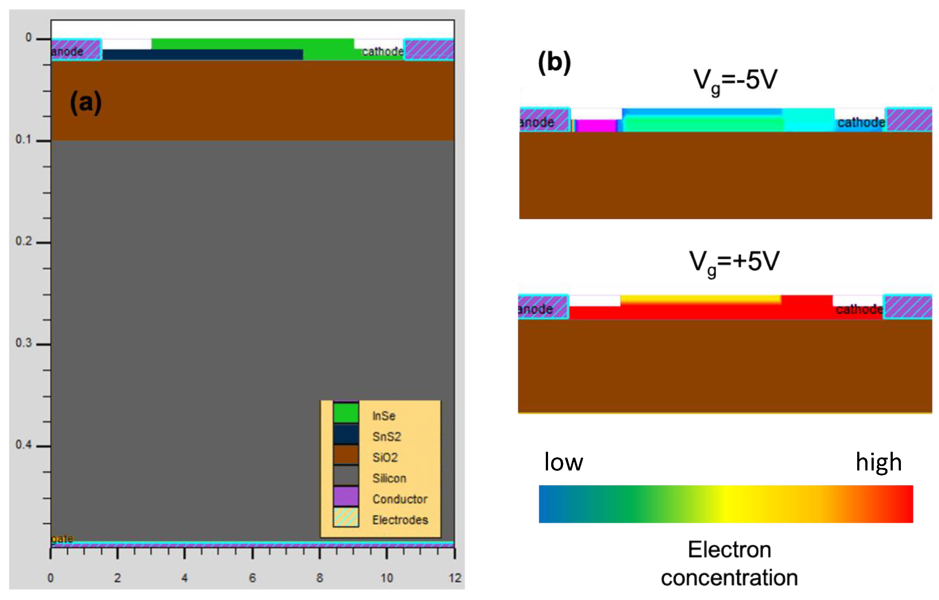
3. Results and Discussion

Figure 1a and b show the schematic and the optical microscope image of the SnS2/InSe photodetector, respectively, which has a channel length (L) of about 20 μm. Figure 1c shows the X-ray diffraction spectrum of the SnS2 crystals grown by the CVT technique. Comparing this pattern with standard tables [22] indicates suitable crystal quality. Figure 1d demonstrates the Raman spectrum including the A1g characteristic peak of SnS2 at 314 cm−1 [23].
The energy band diagram of the device is shown in Figure 2a. Due to small differences in their work functions, electron transfer from InSe to SnS2 results in a small potential barrier (around 40 meV) and linear current versus voltage behavior (Figure 2b). Figure 2c shows the device drain current versus gate voltage. It behaves like an n-type transistor, as we expect based on type of carriers in both layers. The on/off current ratio is about 40, which indicates proper gate modulation in the field effect transistor. The equation μ = [dIsd/dVg] × [L/(W × C × Vsd)] [24] has been used to calculate the field-effect mobility of the charge carriers. The maximum mobility was about 6 cm2/Vs for our device with length, L = 20 μm and width, W = 30 μm for device channel, and C as the capacitance/m2 of the gate oxide about C = 1.15 × 10⁻⁴ F/m2 for the silicon substrate with 300 nm SiO2 dielectric layer. Here, Vg, Vsd, and Isd represent the applied back gate voltage, source-drain voltage, and current respectively. According to Figure 2c (inset), by applying the positive gate voltage (Vg > Vth) the energy band of the layers shift downward, leading to accumulation of electrons within the conduction band of SnS2. Thus, applying a drain voltage results in a high device current, as is shown in the right part of Figure 2c.
The photocurrent (Iph = Ilight − Idark) of the device under illumination by three light sources with wavelengths of 460, 525, and 625 nm at the optical power of 1 µW is shown in Figure 3a. As is shown, shorter wavelengths, or more energetic photons for a given bias voltage, result in higher photocurrent. The depletion charge density can be calculated by QD = C × ∆Vth/e, where C and ΔVth are capacitance and threshold voltage shift, respectively. By using the carrier density, the photogain can be calculated through the G = Iph/(e × QD × S) [25]. According to Figure 3b, the threshold voltage shift is equal to 10 V for 460 and 525 nm wavelength and 5 V for 625 nm wavelength. By applying +70 V gate voltage, the calculated QD are ≈ 7.31 × 1011 cm−2 for both 460 and 525 nm and 3.65 × 1011 cm−2 for 625 nm and photogain are 1.05 × 10¹⁰, 8 × 10⁹, and 7.45 × 10⁹ for 460, 525, and 625 nm, respectively.
The photoresponsivity (R ≡ Iph/Poptical) and detectivity of the devices is presented in Figure 4. As seen in Figure 4a, photoresponsivity at +1 V reaches to 14, 10, and 2.5 mA/W using the three light sources. Detectivity is defined as D* ≡ RS1/2/(2eIdark)1/2 where R is responsivity, S is effective area (here: ~ 600 μm2), and e is elementary charge. Detectivity reaches to 2.2 × 10⁸, 1.6 × 10⁸, and 5 × 10⁷ Junes at 460, 525, and 625 nm at under +1 V respectively. Increasing the charge density and photogain result in the photocurrent enhancement and thus improves the photoresponsivity up to 740 mA/W, 560 mA/W, and 260 mA/W and detectivity up to 3.35 × 10⁹ Junes, 2.55 × 10⁹ Junes, and 1.18 × 10⁹ Junes at Vg = +70 V for 460, 525, and 625 nm, respectively (Figure 4a). As shown in Figure 4b, by applying the gate voltage, the photoresponsivity rises. Therefore, we can control photodetector performance using the gate voltage. By applying a pulsed gate voltage (Figure 4c) without external electronic circuits, the unsaturated state image sensor with real-time tunable gain can be fabricated.
As can be seen, by applying a gate voltage, the photoresponsivity increases up to 50 times, which shows good sensitivity to the gate voltage and shows an improvement compared to similar structures. Table 1 shows a comparison between our devise and the previous reports [26,27,28,29].
To understand the process of light absorption and the mechanism of electron-hole pair generation, this structure was simulated by the Silvaco TCAD software. Figure 5a and b show the simulated structure and the carrier concentration at Vg = −5 and 5 V, respectively. It is observed that at Vg = +5 V the carrier concentration is higher than at Vg= −5 V, which can increase the photocurrent at positive gate voltage. The carrier concentration is calculated through n = σ/eμ where σ is conductivity at Vg [30] and the photocurrent can be calculated by Ipc = eμnEWD, where E and D are the electric field in the channel and absorption depth, respectively [31]. At positive gate voltage, with increasing conduction (in large slope region in Figure 2c), carrier concentration is also increased. This results in a photocurrent enhancement, which had already been observed in experimental results.
The simulated photogeneration at the three wavelengths that were used is shown in Figure 6a. As can be seen, most of the photogeneration is in the SnS2 layer, due to more carriers of n-type SnS2 than InSe. The SnS2 layer has little absorption in the red light range because of rather high energy gap. As a result, in our device, the photocurrent will generate only by absorption of red light in the InSe layer, which causes a photoresponsivity of about 2.5 mA/W. However, in the blue and green light regions, both layers are active, which causes a significant increase in photocurrent and photoresponsivity (14 and 10 A/W for blue and green light). In this way, the SnS2/InSe heterostructure causes the broadband photodetector and works properly in the entire range of the visible light spectrum (Figure 6b).

4. Conclusions

In conclusion, an SnS2/InSe heterostructure photodetector for the visible light spectrum has been introduced. This photodetector presents photoresponsivity from 14 mA/W up to 740 mA/W and detectivity from 2.2 × 10⁸ Jones up to 3.35 × 10⁹ Jones by applying various gate voltages. According to experimental and simulation results, at 460 and 532 nm wavelengths, due to the proximity of the energy of the photon to the SnS2 energy gap, light is absorbed in both layers and the photocurrent increases. Our results showed that the gate voltage increases the carriers in the SnS2 layer. Due to the weak absorption of red light in the SnS2 layer, applying gate voltage does not affect the photocurrent at red light compared to blue and green light. The results show that this structure has potential for use in visible light tunable gain image sensors.

Author Contributions

The authors confirm their contributions as follow; Conceptualization, A.I.z. and S.H.; methodology, S.H.; validation, A.I.z. and S.M.M.; device fabrication, A.E.; investigation, S.H.; resources, A.I.z.; data curation, A.I.z.; writing—original draft preparation, S.H.; writing—review and editing, A.I.z.; visualization, S.H.; project administration, A.I.z. All authors have read and agreed to the published version of the manuscript.

Funding

This research was funded by Iran National Science Foundation (INSF), grant number 99029911.

Data Availability Statement

Not applicable.

Conflicts of Interest

The authors declare no conflict of interest.

References

  1. El Gamal, A. Trends in CMOS image sensor technology and design. In Proceedings of the Technical Digest—International Electron Devices Meeting, San Francisco, CA, USA, 8–11 December 2002; pp. 805–808. [Google Scholar] [CrossRef] [Green Version]
  2. Sakai, T.; Takagi, T.; Imamura, K.; Mineo, K.; Yakushiji, H.; Hashimoto, Y.; Aotake, T.; Sadamitsu, Y.; Sato, H.; Aihara, S. Color-Filter-Free Three-Layer-Stacked Image Sensor Using Blue/Green-Selective Organic Photoconductive Films with Thin-Film Transistor Circuits on CMOS Image Sensors. ACS Appl. Electron. Mater. 2021, 3, 3085–3095. [Google Scholar] [CrossRef]
  3. Cho, K.; Lee, S.J.; Kavehei, O.; Eshraghian, K. High fill factor low-voltage CMOS image sensor based on time-to-threshold PWM VLSI architecture. IEEE Trans. Very Large Scale Integr. (VLSI) Syst. 2014, 22, 1548–1556. [Google Scholar] [CrossRef]
  4. Chou, W.F.; Yeh, S.F.; Chiu, C.F.; Hsieh, C.C. A linear-logarithmic CMOS image sensor with pixel-FPN reduction and tunable response curve. IEEE Sens. J. 2014, 14, 1625–1632. [Google Scholar] [CrossRef]
  5. Blanksby, A.J.; Loinaz, M.J. Performance analysis of a color CMOS photogate image sensor. IEEE Trans. Electron Devices 2000, 47, 55–64. [Google Scholar] [CrossRef]
  6. Tsai, T.H.; Sahoo, A.K.; Syu, H.K.; Wu, Y.C.; Tsai, M.Y.; Siao, M.D.; Yang, Y.C.; Lin, Y.F.; Liu, R.S.; Chiu, P.W. WS2/WSe2Nanodot Composite Photodetectors for Fast and Sensitive Light Detection. ACS Appl. Electron. Mater. 2021, 3, 4291–4299. [Google Scholar] [CrossRef]
  7. Kallis, K.T.; Müller, M.R.; Knoch, J.; Gumprich, A.; Merten, D. Electrostatic Doping of 2D-Materials—From Single Devices Toward Circuitry Exploration. Quantum Matter 2017, 6, 45–49. [Google Scholar] [CrossRef]
  8. Liu, J.; Zhong, M.; Liu, X.; Sun, G.; Chen, P.; Zhang, Z.; Li, J.; Ma, H.; Zhao, B.; Wu, R.; et al. Two-dimensional plumbum-doped tin diselenide monolayer transistor with high on/off ratio. Nanotechnology 2018, 29, 474002. [Google Scholar] [CrossRef]
  9. McGuire, F.A.; Lin, Y.-C.; Price, K.; Rayner, G.B.; Khandelwal, S.; Salahuddin, S.; Franklin, A.D. Sustained Sub-60 mV/decade switching via the negative capacitance effect in MoS2 Transistors. Nano Lett. 2017, 17, 4801–4806. [Google Scholar] [CrossRef]
  10. Wang, F.; Liu, Z.; Zhang, T.; Long, M.; Wang, X.; Xie, R.; Ge, H.; Wang, H.; Hou, J.; Gu, Y.; et al. Fully Depleted Self-Aligned Heterosandwiched Van Der Waals Photodetectors. Adv. Mater. 2022, 34, 2203283. [Google Scholar] [CrossRef]
  11. Lei, T.; Tu, H.; Lv, W.; Ma, H.; Wang, J.; Hu, R.; Wang, Q.; Zhang, L.; Fang, B.; Liu, Z.; et al. Ambipolar Photoresponsivity in an Ultrasensitive Photodetector Based on a WSe2/InSe Heterostructure by a Photogating Effect. ACS Appl. Mater. Interfaces 2021, 13, 50213–50219. [Google Scholar] [CrossRef]
  12. Liu, Y.; Xia, Q.; He, J.; Liu, Z. Direct Observation of High Photoresponsivity in Pure Graphene Photodetectors. Nanoscale Res. Lett. 2017, 12, 93. [Google Scholar] [CrossRef] [Green Version]
  13. Sarker, B.K.; Childres, I.; Cazalas, E.; Jovanovic, I.; Chen, Y.P. Gate-tunable and high responsivity graphene phototransistors on undoped semiconductor substrates. arXiv 2014, arXiv:1409.5725. [Google Scholar] [CrossRef]
  14. Jahangir, I.; Uddin, M.A.; Franken, A.; Singh, A.K.; Koley, G. Electrically or chemically tunable photodetector with ultra high responsivity using graphene/InN nanowire based mixed dimensional barristors. Nanotechnology 2021, 32, 475203. [Google Scholar] [CrossRef]
  15. Xu, J.; Chen, L.; Dai, Y.-W.; Cao, Q.; Sun, Q.-Q.; Ding, S.-J.; Zhu, H.; Zhang, D.W. A two-dimensional semiconductor transistor with boosted gate control and sensing ability. Sci. Adv. 2017, 3, e1602246. [Google Scholar] [CrossRef] [Green Version]
  16. Bandurin, D.A.; Tyurnina, A.V.; Yu, G.L.; Mishchenko, A.; Zólyomi, V.; Morozov, S.; Kumar, R.K.; Gorbachev, R.; Kudrynskyi, Z.; Pezzini, S.; et al. High electron mobility, quantum Hall effect and anomalous optical response in atomically thin InSe. Nat. Nanotechnol. 2016, 12, 223–227. [Google Scholar] [CrossRef]
  17. Mudd, G.W.; Svatek, S.A.; Ren, T.; Patanè, A.; Makarovsky, O.; Eaves, L.; Beton, P.H.; Kovalyuk, Z.D.; Lashkarev, G.V.; Kudrynskyi, Z.R.; et al. Tuning the Bandgap of Exfoliated InSe Nanosheets by Quantum Confinement. Adv. Mater. 2013, 25, 5714–5718. [Google Scholar] [CrossRef] [Green Version]
  18. Gonzalez, J.M.; Oleynik, I.I. Layer-dependent properties of SnS2 and SnSe2 two-dimensional materials. Phys. Rev. B 2016, 94, 125443. [Google Scholar] [CrossRef] [Green Version]
  19. Hosseini, S.A.; Esfandiar, A.; Zad, A.I.; Hosseini-Shokouh, S.H.; Mahdavi, S.M. High-Photoresponsive Backward Diode by Two-Dimensional SnS2/Silicon Heterostructure. ACS Photonics 2019, 6, 728–734. [Google Scholar] [CrossRef]
  20. Gao, E.; Lin, S.Z.; Qin, Z.; Buehler, M.J.; Feng, X.Q.; Xu, Z. Mechanical exfoliation of two-dimensional materials. J. Mech. Phys. Solids 2018, 115, 248–262. [Google Scholar] [CrossRef]
  21. Kim, S.; Shin, S.; Kim, T.; Du, H.; Song, M.; Lee, C.; Kim, K.; Cho, S.; Seo, D.H.; Seo, S. Robust graphene wet transfer process through low molecular weight polymethylmethacrylate. Carbon N Y 2016, 98, 352–357. [Google Scholar] [CrossRef]
  22. Persson, K. Materials Data on SnS2 (SG:164) by Materials Project. 2014. Available online: https://materialsproject.org/materials/mp-1170/ (accessed on 26 July 2021).
  23. Sriv, T.; Kim, K.; Cheong, H. Low-Frequency Raman Spectroscopy of Few-Layer 2H-SnS 2. Sci. Rep. 2018, 8, 10194. [Google Scholar] [CrossRef] [PubMed] [Green Version]
  24. Huang, J.; Yang, L.; Liu, D.; Chen, J.; Fu, Q.; Xiong, Y.; Lin, F.; Xiang, B. Large-area synthesis of monolayer WSe2 on a SiO2/Si substrate and its device applications. Nanoscale 2015, 7, 4193–4198. [Google Scholar] [CrossRef] [PubMed]
  25. Lee, I.; Rathi, S.; Lim, D.; Li, L.; Park, J.; Lee, Y.; Yi, K.S.; Dhakal, K.P.; Kim, J.; Lee, C.; et al. Gate-Tunable Hole and Electron Carrier Transport in Atomically Thin Dual-Channel WSe2/MoS2 Heterostructure for Ambipolar Field-Effect Transistors. Adv. Mater. 2016, 28, 9519–9525. [Google Scholar] [CrossRef] [PubMed]
  26. Zhang, W.; Chuu, C.-P.; Huang, J.-K.; Chen, C.-H.; Tsai, M.-L.; Chang, Y.-H.; Liang, C.-T.; Chen, Y.-Z.; Chueh, Y.-L.; He, J.-H.; et al. Ultrahigh-gain photodetectors based on atomically thin graphene-MoS2 heterostructures. Sci. Rep. 2014, 4, 3826. [Google Scholar] [CrossRef] [Green Version]
  27. Feng, W.; Wu, J.-B.; Li, X.; Zheng, W.; Zhou, X.; Xiao, K.; Cao, W.; Yang, B.; Idrobo, J.-C.; Basile, L.; et al. Ultrahigh photo-responsivity and detectivity in multilayer InSe nanosheets phototransistors with broadband response. J. Mater. Chem. C 2015, 3, 7022–7028. [Google Scholar] [CrossRef]
  28. Yu, J.; Suleiman, A.A.; Zheng, Z.; Zhou, X.; Zhai, T. Giant-Enhanced SnS2 Photodetectors with Broadband Response through Oxygen Plasma Treatment. Adv. Funct. Mater. 2020, 30, 2001650. [Google Scholar] [CrossRef]
  29. Zhao, Y.; Cho, J.; Choi, M.; Coileáin, C.; Arora, S.; Hung, K.-M.; Chang, C.-R.; Abid, M.; Wu, H.-C. Light-Tunable Polarity and Erasable Physisorption-Induced Memory Effect in Vertically Stacked InSe/SnS2 Self-Powered Photodetector. ACS Nano 2022, 16, 17347–17355. [Google Scholar] [CrossRef]
  30. Mondal, P.; Bid, A.; Basu, J.K. Electrical and Chemical Tuning of Exciton Lifetime in Monolayer MoS2 for Field-Effect Transistors. ACS Appl. Nano Mater 2019, 3, 641–647. [Google Scholar] [CrossRef] [Green Version]
  31. Island, J.O.; Blanter, S.I.; Buscema, M.; van der Zant, H.S.J.; Castellanos-Gomez, A. Gate controlled photocurrent generation mechanisms in high-gain In2Se3 phototransistors. Nano Lett. 2015, 15, 7853–7858. [Google Scholar] [CrossRef]
Figure 1. (a) Schematic of SnS2/InSe photodetector. (b) Optical microscope image of the fabricated device. (c) XRD spectrum of the SnS2 Crystal. (d) Raman Spectrum of the SnS2 layer.
Micromachines 13 02068 g001
Figure 2. (a) Band diagram of SnS2/InSe heterostructure before and after contact, after contact, electron transfer from InSe to SnS2 and hole transfer from SnS2 to InSe (Ef, Ec, and Ev are Fermi level, conduction band edge, and vallance band edge, respectively, The energy values are shown in figure). (b) Typical current-voltage curve of the device. (c) Drain current versus gate voltage of the device. Inset presents band diagram in positive gate voltage.
Micromachines 13 02068 g002
Figure 3. (a) Photocurrent of the device under light irradiation. (b) The transfer curves in light irradiations.
Micromachines 13 02068 g003
Figure 4. (a) photoresponsivity and photodetectivity of the device under light irradiation by applying and without applying gate voltage; (b) photoresponsivity versus gate voltage under red, green and blue light irradiation (c) photocurrent of the device under pulsed applying gate voltages at different wavelength irradiation (green is applying +70 V gate voltage and red is without gate voltage).
Micromachines 13 02068 g004
Figure 5. (a) Schematic of the simulated structure (500 nm × 12 μm). (b) Carrier concentration at positive and negative gate voltage in the channel.
Micromachines 13 02068 g005
Figure 6. (a) Simulated photogeneratin at 625 nm, 525 nm and 460 nm wavelength. (b) Band diagram of device in light irradiation.
Micromachines 13 02068 g006
Table 1. Comparison of gate effect on 2D photodetectors.
StructureGainPhotoresponsivity Ratio
(Applying Gate/without Applying Gate)
Response Wavelength (nm)References
Graphene1151.16632[12]
Graphene/InN-4550[14]
Graphene/MoS21085650[26]
InSe-2.5254~850[27]
SnS2-3300~750[28]
SnS2/InSe-1.4405[29]
SnS2/InSe101052460~625This Work
Publisher’s Note: MDPI stays neutral with regard to jurisdictional claims in published maps and institutional affiliations.

