

High-Density 1R/1W Dual-Port Spin-Transfer Torque MRAM


Abstract
:1. Introduction
2. Review of Conventional STT-MRAMs
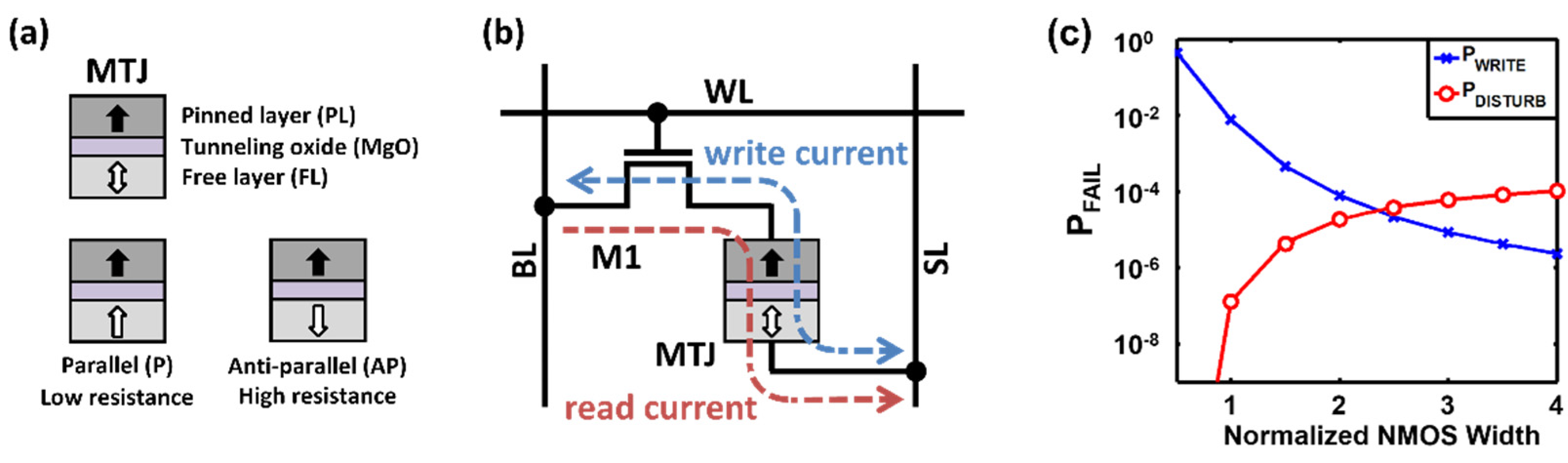
2.1. Single-Port STT-MRAM
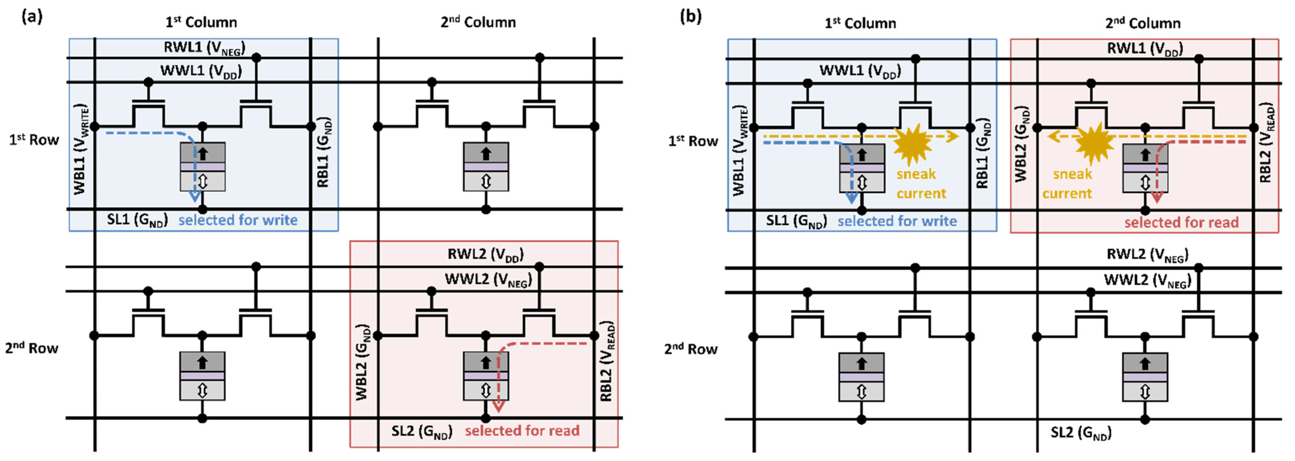
2.2. 1R/1W Dual-Port STT-MRAM
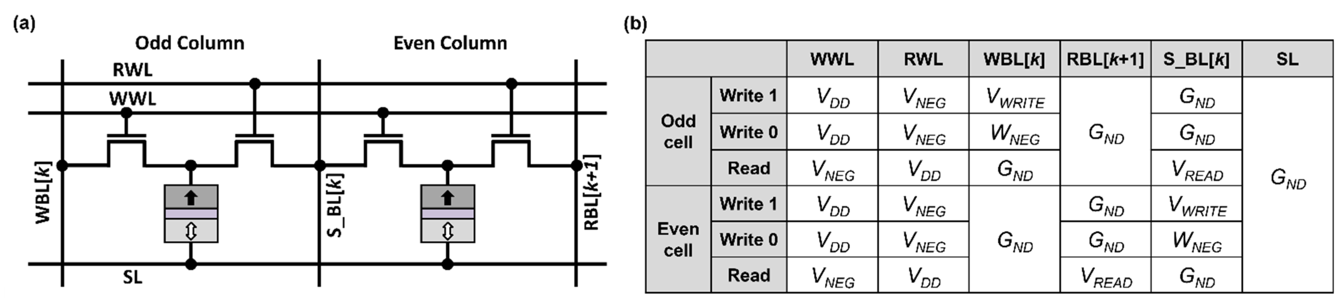
3. Proposed Design
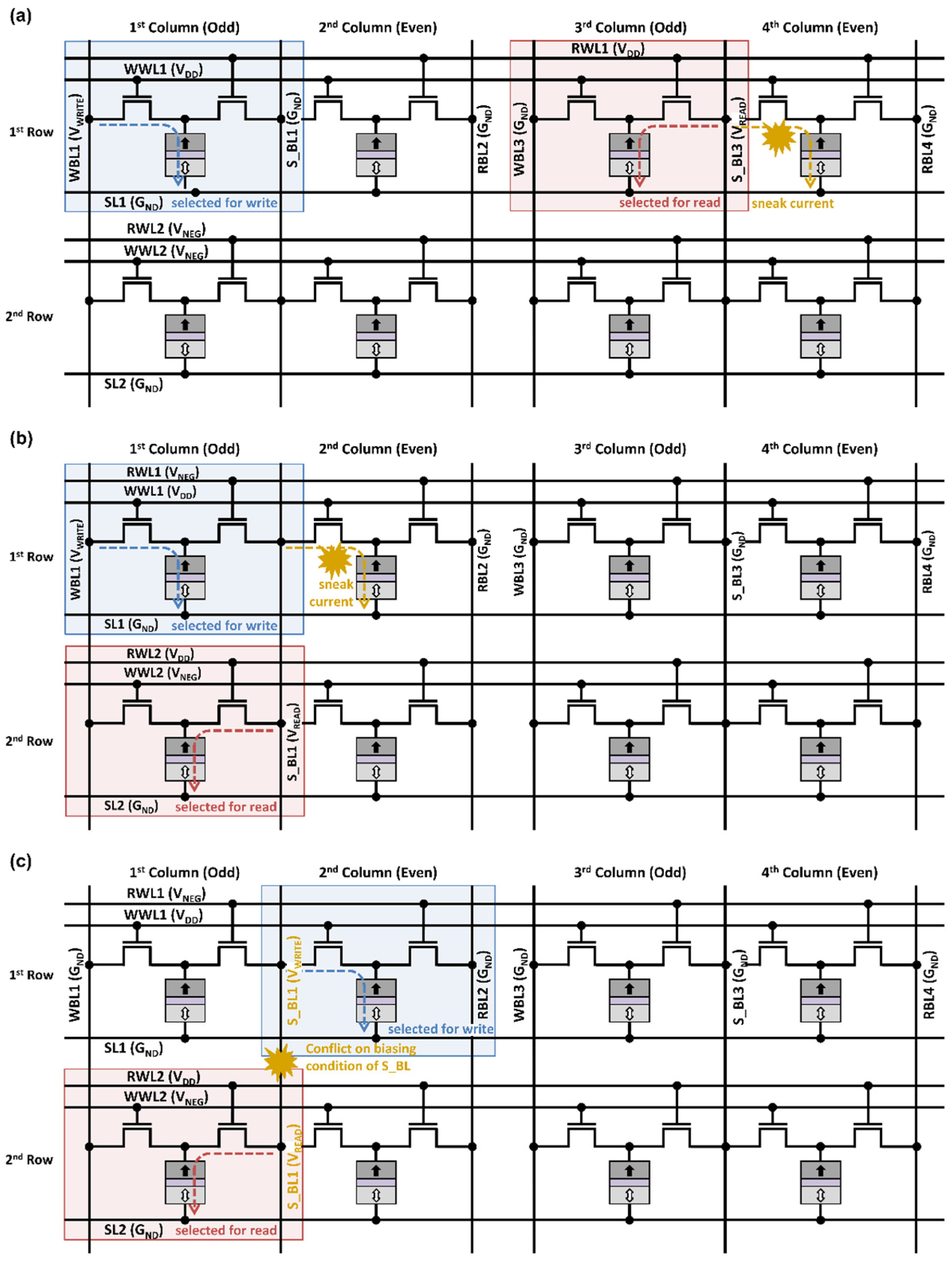
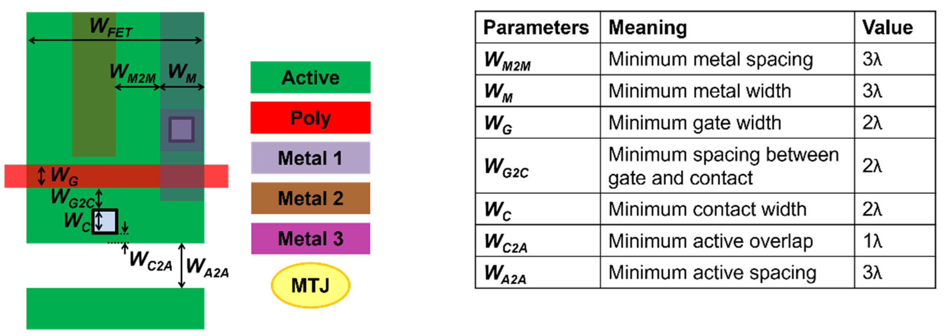
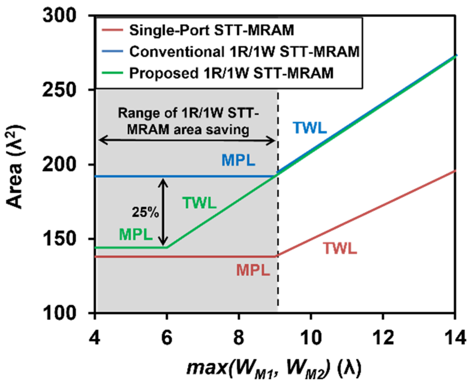
4. Layout Analysis
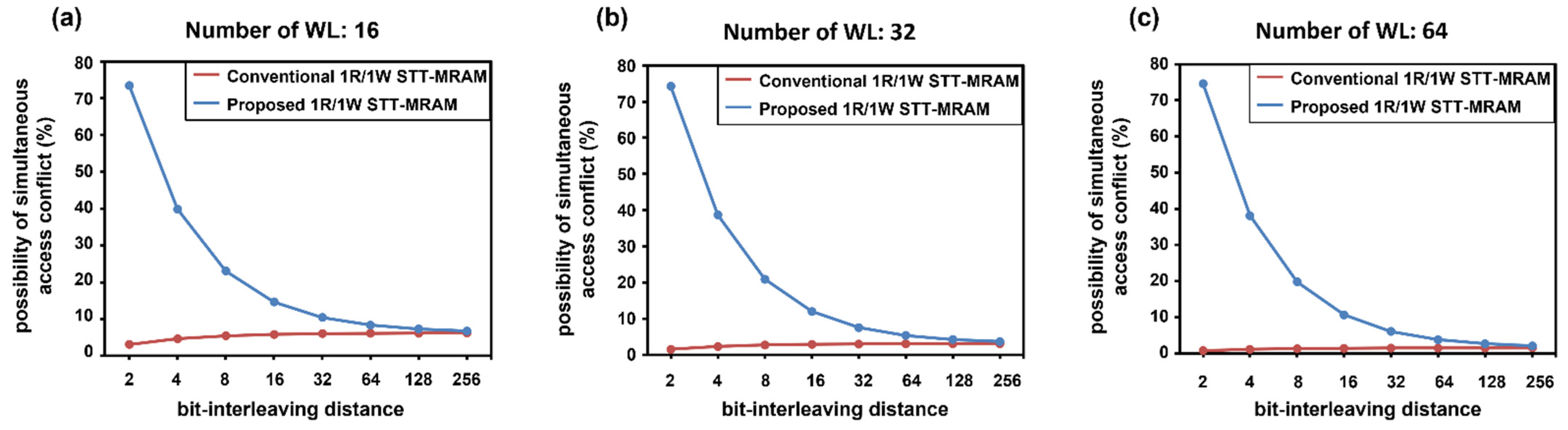
5. Simulations and Results
- (1)
- (2)
- the non-equilibrium Green’s function (NEGF) formalism in order to determine the resistivity of MTJ [24];
- (3)
- the simulation program with integrated circuit emphasis (SPICE) simulator to model the memory bit-cell circuit.
6. Conclusions
Author Contributions
Funding
Conflicts of Interest
References
- Chun, K.C.; Zhao, H.; Harms, J.D.; Kim, T.-H.; Wang, J.-P.; Kim, C.H. A scaling roadmap and performance evaluation of in plane and perpendicular MTJ based STT-MRAMs for high-density cache memory. IEEE J. Solid State Circuits 2013, 48, 598–610. [Google Scholar] [CrossRef]
- Augustine, C.; Mojumder, N.; Fong, X.; Choday, H.; Park, S.P.; Roy, K. STT-MRAMs for future universal memories: Perspective and prospective. In Proceedings of the International Conference on Microelectronics, Nis, Serbia, 13–16 May 2012; pp. 349–355. [Google Scholar] [CrossRef]
- Li, J.; Ndai, P.; Goel, A.; Salahuddin, S.; Roy, K. Design paradigm for robust spin-torque transfer magnetic RAM (STT MRAM) from circuit/architecture perspective. IEEE Trans. Very Large Scale Integr. (VLSI) Syst. 2009, 18, 1710–1723. [Google Scholar] [CrossRef]
- Fong, X.; Kim, Y.; Choday, S.H.; Roy, K. Failure mitigation techniques for 1T-1MTJ spin-transfer torque MRAM bit-cells. IEEE Trans. Very Large Scale Integr. (VLSI) Syst. 2014, 22, 384–395. [Google Scholar] [CrossRef]
- Lin, C.J.; Kang, S.H.; Wang, Y.J.; Lee, K.; Zhu, X.; Chen, W.C.; Li, X.; Hsu, W.N.; Kao, Y.C.; Tran, L.; et al. 45 nm low power CMOS logic compatible embedded STT MRAM utilizing a reverse-connection 1T/1MTJ cell. In Proceedings of the IEEE International Electron Devices Meeting, Baltimore, MD, USA, 7–9 December 2009; pp. 11.6.1–11.6.4. [Google Scholar] [CrossRef]
- Seo, Y.; Fong, X.; Roy, K. Domain wall coupling-based STT-MRAM for on-chip cache applications. IEEE Trans. Electron. Devices 2015, 62, 554–560. [Google Scholar] [CrossRef]
- Park, S.P.; Gupta, S.; Mojunder, N.; Raghunathan, A.; Roy, K. Future cache design using STT MRAMs for improved energy efficiency: Devices, circuits and architecture. In Proceedings of the ACM/EDAC/IEEE Design Automation Conference, San Francisco, CA, USA, 3–7 June 2012; pp. 492–497. [Google Scholar] [CrossRef]
- Augustine, C.; Raychowdhury, A.; Somasekhar, D.; Tschanz, J.; Roy, K.; De, V.K. Numerical analysis of typical STT-MTJ stacks for 1T-1R memory arrays. In Proceedings of the IEEE International Electron Devices Meeting, San Francisco, CA, USA, 6–8 December 2010; pp. 22.7.1–22.7.4. [Google Scholar] [CrossRef]
- Kim, Y.; Gupta, S.K.; Park, S.P.; Panagopoulos, G.; Roy, K. Write-optimized reliable design of STT MRAM. In Proceedings of the ACM/IEEE International Symposium on Low Power Electronics and Design, Redondo Beach, CA, USA, 30 July–1 August 2012; pp. 3–8. [Google Scholar] [CrossRef]
- Seo, Y.; Kwon, K.-W.; Fong, X.; Roy, K. High Performance and Energy-Efficient On-Chip Cache Using Dual Port (1R/1W) Spin-Orbit Torque MRAM. IEEE J. Emerg. Sel. Top. Circuits Syst. 2016, 6, 293–304. [Google Scholar] [CrossRef]
- Bi, X.; Weldon, M.A.; Li, H. STT-RAM designs supporting dual-port accesses. In Proceedings of the Design, Automation & Test in Europe Conference & Exhibition, Grenoble, France, 18–22 March 2013; pp. 1–6. [Google Scholar] [CrossRef]
- Seo, Y.; Fong, X.; Kwon, K.-W.; Roy, K. Spin-Hall Magnetic Random-Access Memory with Dual Read/Write Ports for On-Chip Caches. IEEE Magn. Lett. 2015, 6, 3000204. [Google Scholar] [CrossRef]
- Seo, Y.; Kwon, K.-W. Area Optimization Techniques for High-Density Spin-Orbit Torque MRAMs. Electronics 2021, 10, 792. [Google Scholar] [CrossRef]
- Nayak, D.; Acharya, D.P.; Nanda, U. A high sTable 8T-SRAM with bit interleaving capability for minimization of soft error rate. Microelectron. J. 2018, 73, 43–51. [Google Scholar] [CrossRef]
- Baeg, S.; Wen, S.; Wong, R. SRAM Interleaving Distance Selection With a Soft Error Failure Model. IEEE Trans. Nucl. Sci. 2009, 56, 2111–2118. [Google Scholar] [CrossRef]
- Shi, Y.Q.; Zhang, X.M.; Ni, Z.-C.; Ansari, N. Interleaving for combating bursts of errors. IEEE Circuits Syst. Mag. 2004, 4, 29–42. [Google Scholar] [CrossRef]
- Gupta, S.K.; Park, S.P.; Mojumder, N.N.; Roy, K. Layout-aware optimization of STT-MRAMs. In Proceedings of the Design, Automation & Test in Europe Conference & Exhibition, Dresden, Germany, 12–16 March 2012; pp. 1455–1458. [Google Scholar] [CrossRef]
- Seo, Y.; Kwon, K.-W. Area-optimized design of SOT-MRAM. IEICE Electron. Express 2020, 17, 20200314. [Google Scholar] [CrossRef]
- Liebman, L. DfM, the teenage years. Proc. SPIE 2008, 6925, 692502. [Google Scholar] [CrossRef]
- Fong, X.; Gupta, S.K.; Mojumder, N.N.; Choday, S.H.; Augustine, C.; Roy, K. KNACK: A Hybrid Spin-Charge Mixed-Mode Simulator for Evaluating Different Genres of Spin Transfer Torque MRAM Bit-cells. In Proceedings of the International Conference on Simulation of Semiconductor Processes and Devices, Osaka, Japan, 8–10 September 2011; pp. 51–54. [Google Scholar] [CrossRef]
- Gilbert, T.L. A phenomenological theory of damping in ferromagnetic materials. IEEE Trans. Magn. 2004, 40, 3443–3449. [Google Scholar] [CrossRef]
- Fong, X.; Kim, Y.; Venkatesan, R.; Choday, S.H.; Raghunathan, A.; Roy, K. Spin-Transfer Torque Memories: Devices, Circuits, and Systems. Proc. IEEE 2016, 104, 1449–1488. [Google Scholar] [CrossRef]
- Ikeda, S.; Miura, K.; Yamamoto, H.; Mizunuma, K.; Gan, H.D.; Endo, M.; Kanai, S.; Hayakawa, J.; Ohno, H. A perpendicular-anisotropy CoFeB-MgO magnetic tunnel junction. Nat. Mater. 2010, 9, 721–724. [Google Scholar] [CrossRef] [PubMed]
- Datta, D.; Behin-Aein, D.; Salahuddin, S.; Datta, S. Quantitative Model for TMR and Spin-Transfer Torque in MTJ Devices. In Proceedings of the IEEE International Electron Devices Meeting, San Francisco, CA, USA, 6–8 December 2010; pp. 22.8.1–22.8.4. [Google Scholar] [CrossRef]
- Mojumder, N.N.; Augustine, C.; Nikonov, D.E.; Roy, K. Electronic transport and effect of quantum confinement in dual barrier resonant tunneling spin-torque-transfer magnetic tunnel junctions. J. Appl. Phys. 2010, 108, 104306.1–104306.12. [Google Scholar] [CrossRef]
- Kishi, T.; Yoda, H.; Kai, T.; Nagase, T.; Kitagawa, E.; Yoshikawa, M.; Nishiyama, K.; Daibou, T.; Nagamine, M.; Amano, M.; et al. Lower-current and fast switching of a perpendicular TMR for high speed and high density spin-transfer-torque MRAM. In Proceedings of the IEEE International Electron Devices Meeting, San Francisco, CA, USA, 15–17 December 2008; pp. 1–4. [Google Scholar] [CrossRef]


| Device Parameters | Magnetic Tunnel Junction |
|---|---|
| Activation Energy, EA | 56 kBT |
| Gilbert damping, α | 0.01 |
| Saturation magnetization, MS | 1000 × 103 A/m |
| Dimension of FL (WFL × LFL × tFL) | 40 nm × 40 nm × 2 nm 1 |
| Tunneling oxide barrier thickness, tMgO | 1.25 nm |
| Critical current for 10 ns switching time | 27 µA |
| Conventional Single-Port STT-MRAM | Conventional 1R/1W STT-MRAM | Proposed 1R/1W STT-MRAM | |
|---|---|---|---|
| Transistor width (nm) | 180 | 180 (M1)/60 (M2) | 120 (M1)/60 (M2) |
| Bit-cell area (µm2) | 0.0552 | 0.0768 | 0.0576 |
| VWRITE (V) | 0.8 | 0.8 | 1.0 |
| VREAD (V) | 0.2 | 0.2 | 0.2 |
| VNEG (V) | - | −0.8 | −0.8 |
| Write Power (µW) | 30.15 | 30.99 | 32.48 |
| Read Power (µW) | 4.00 | 3.40 | 3.40 |
| Read-Disturb Margin (%) | 48 | 57 | 57 |
Publisher’s Note: MDPI stays neutral with regard to jurisdictional claims in published maps and institutional affiliations. |
© 2022 by the authors. Licensee MDPI, Basel, Switzerland. This article is an open access article distributed under the terms and conditions of the Creative Commons Attribution (CC BY) license (https://creativecommons.org/licenses/by/4.0/).
Share and Cite
Seo, Y.; Kwon, K.-W. High-Density 1R/1W Dual-Port Spin-Transfer Torque MRAM. Micromachines 2022, 13, 2224. https://doi.org/10.3390/mi13122224
Seo Y, Kwon K-W. High-Density 1R/1W Dual-Port Spin-Transfer Torque MRAM. Micromachines. 2022; 13(12):2224. https://doi.org/10.3390/mi13122224
Chicago/Turabian StyleSeo, Yeongkyo, and Kon-Woo Kwon. 2022. "High-Density 1R/1W Dual-Port Spin-Transfer Torque MRAM" Micromachines 13, no. 12: 2224. https://doi.org/10.3390/mi13122224
APA StyleSeo, Y., & Kwon, K.-W. (2022). High-Density 1R/1W Dual-Port Spin-Transfer Torque MRAM. Micromachines, 13(12), 2224. https://doi.org/10.3390/mi13122224