
Reflow Soldering Capability Improvement by Utilizing TaN Interfacial Layer in 1Mbit RRAM Chip

Abstract
:1. Introduction
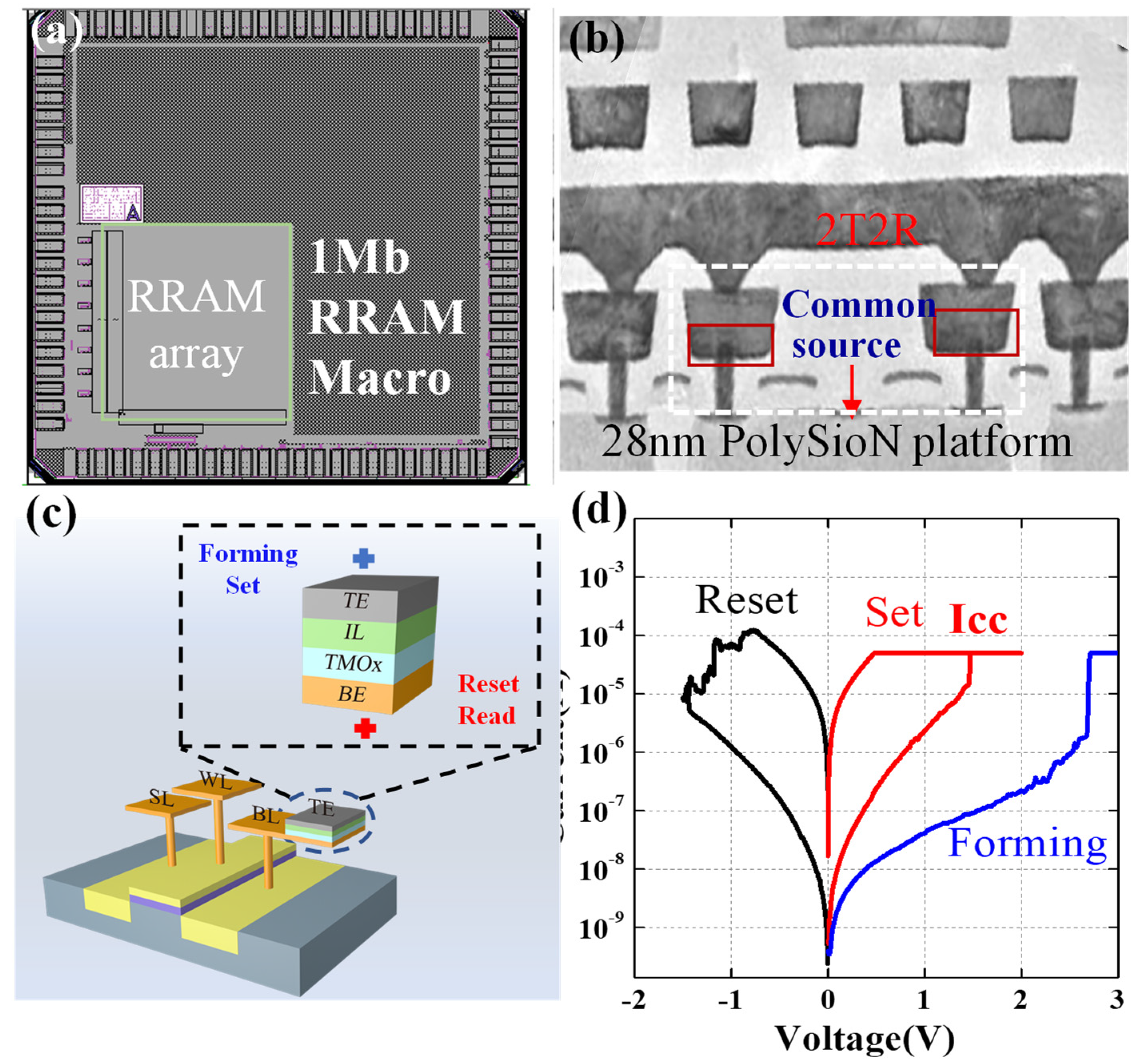
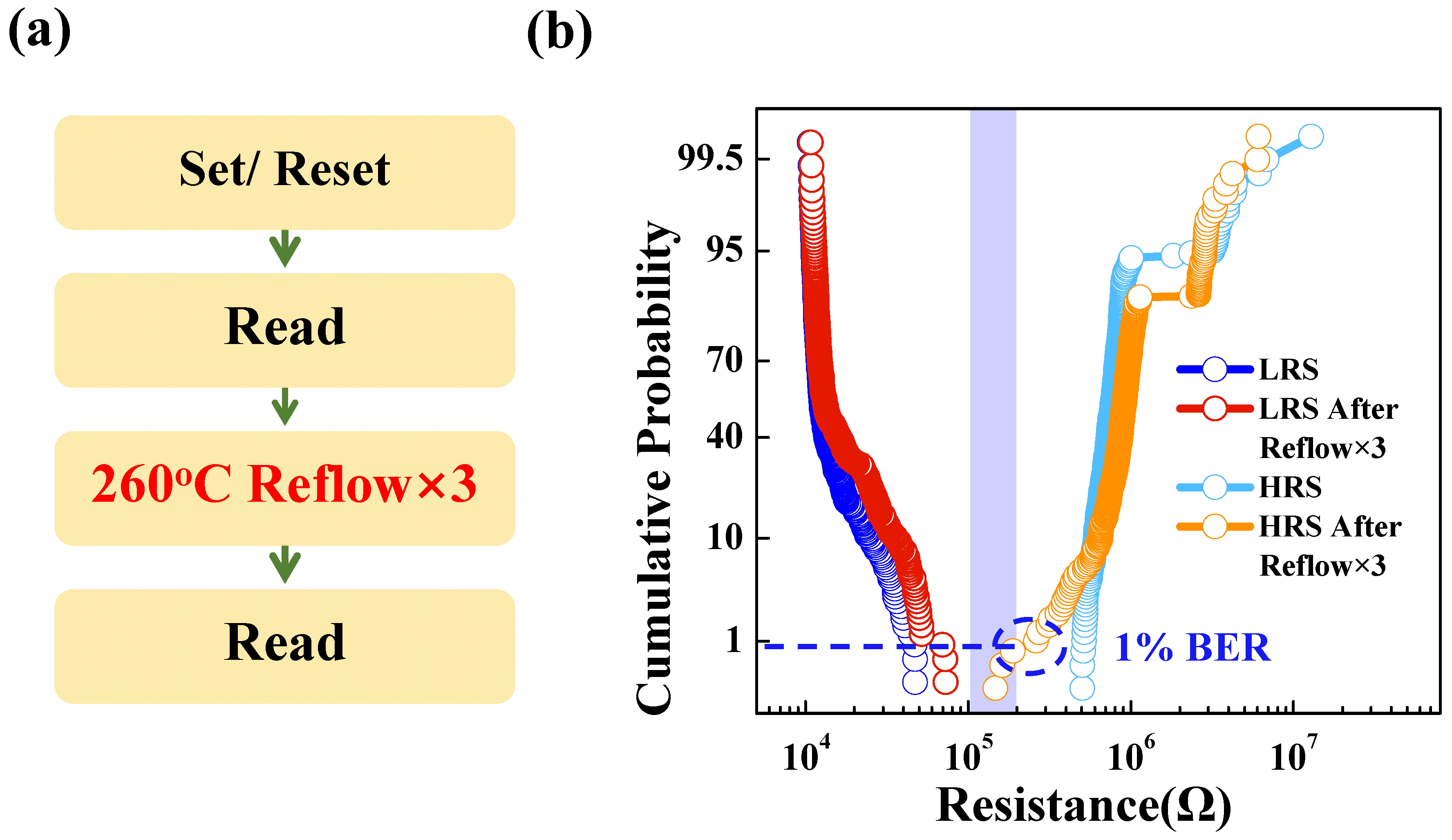
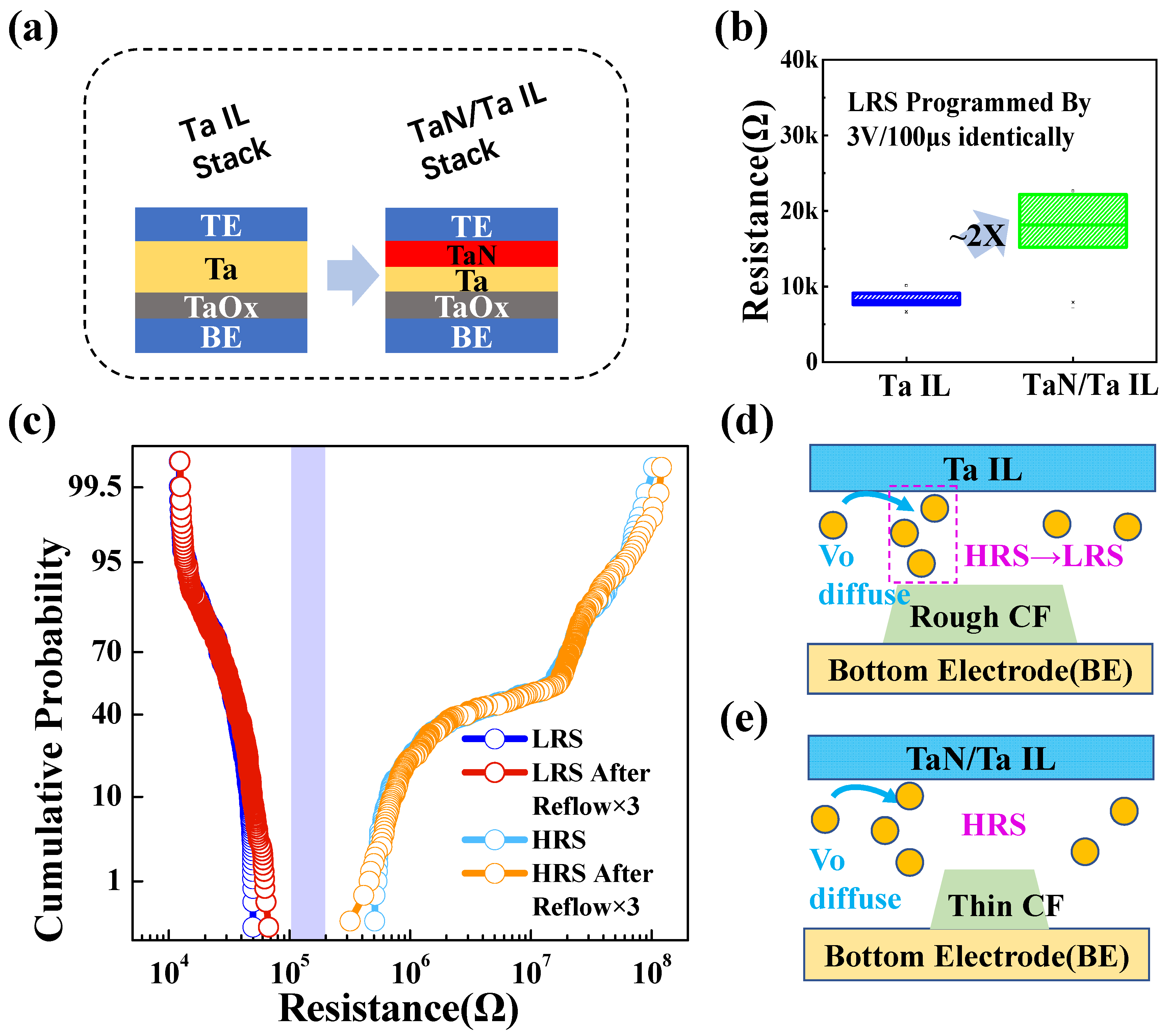
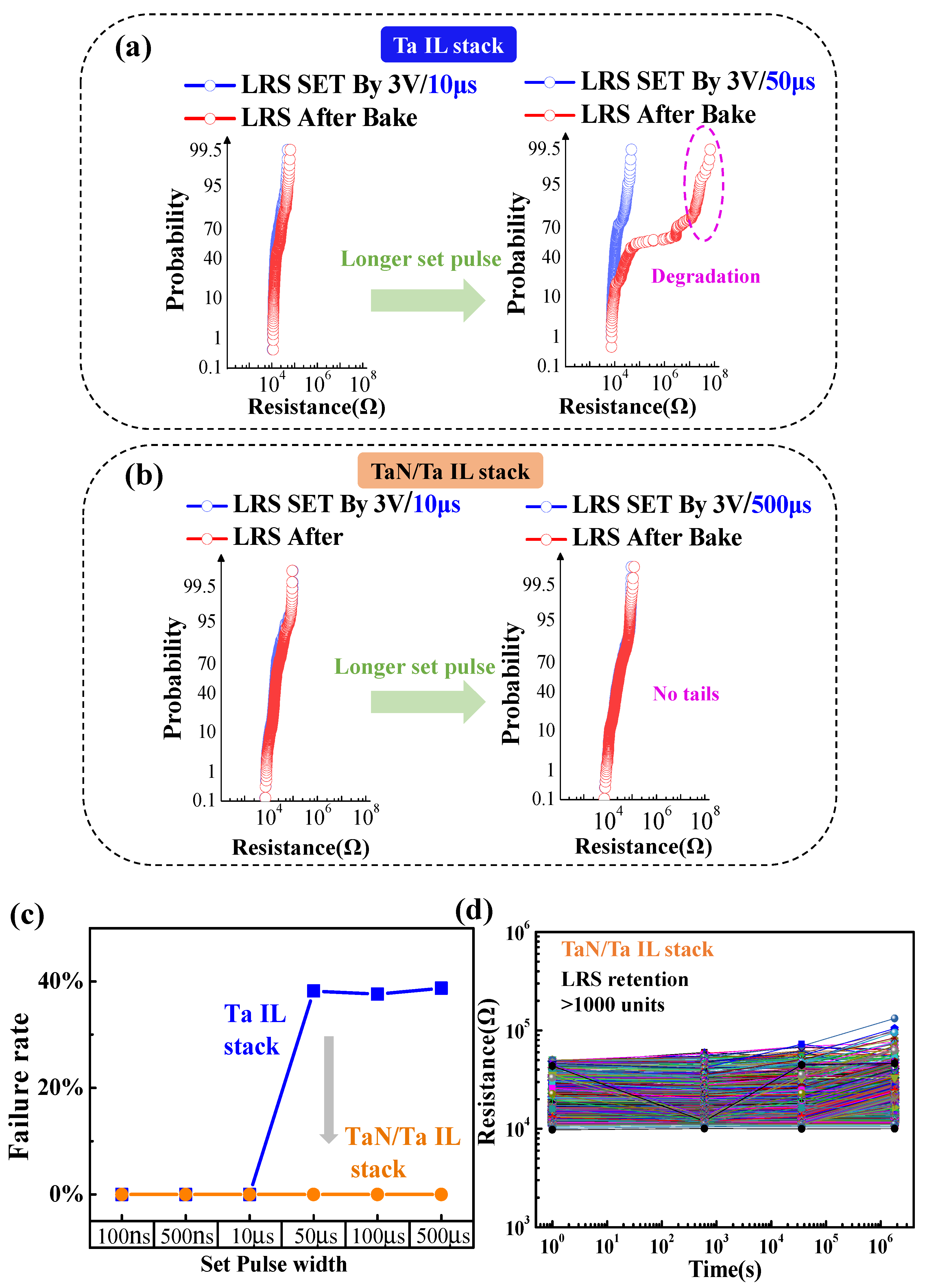
2. Experiment
3. Results and Discussion
4. Conclusions
Author Contributions
Funding
Data Availability Statement
Conflicts of Interest
References
- Xu, X.; Luo, Q.; Gong, T.; Lv, H.; Long, S.; Liu, Q.; Chung, S.S.; Li, J.; Liu, M. Fully CMOS compatible 3D vertical RRAM with self-aligned self-selective cell enabling sub-5 nm scaling. In Proceedings of the 2016 IEEE Symposium on VLSI Technology, Honolulu, HI, USA, 14–16 June 2016; pp. 1–2. [Google Scholar]
- Ho, C.; Shen, T.Y.; Hsu, P.Y.; Chang, S.C.; Wen, S.Y.; Lin, M.H.; Wang, P.K.; Liao, S.C.; Chou, C.S.; Peng, K.M.; et al. Random soft error suppression by stoichiometric engineering: CMOS compatible and reliable 1Mb HfO2-ReRAM with 2 extra masks for embedded IoT systems. In Proceedings of the 2016 IEEE Symposium on VLSI Technology, Honolulu, HI, USA, 14–16 June 2016; pp. 1–2. [Google Scholar]
- Ho, C.; Chang, S.-C.; Huang, C.-Y.; Lim, S.-F.; Hsieh, M.-H.; Chang, S.-C.; Liao, H.-H. Integrated HfO2-RRAM to achieve highly reliable, greener, faster, cost-effective, and scaled devices. In Proceedings of the 2017 IEEE International Electron Devices Meeting (IEDM), San Francisco, CA, USA, 2–6 December 2017; pp. 2.6.1–2.6.4. [Google Scholar]
- Shih, M.C.; Wang, C.Y.; Lee, Y.H.; Wang, W.; Thomas, L.; Liu, H.; Zhu, J.; Lee, Y.J.; Jan, G.; Wang, Y.J.; et al. Reliability study of perpendicular STT-MRAM as emerging embedded memory qualified for reflow soldering at 260 °C. In Proceedings of the 2016 IEEE Symposium on VLSI Technology, Honolulu, HI, USA, 14–16 June 2016. [Google Scholar]
- Shih, Y.-C.; Lee, C.-F.; Chang, Y.-A.; Lee, P.-H.; Lin, H.-J.; Chen, Y.-L.; Lo, C.-P.; Lin, K.-F.; Chiang, T.-W.; Lee, Y.-J.; et al. A Reflow-capable, Embedded 8Mb STT-MRAM Macro with 9nS Read Access Time in 16nm FinFET Logic CMOS Process. In Proceedings of the 2020 IEEE International Electron Devices Meeting (IEDM), Virtually, 12–18 December 2020; pp. 11.4.1–11.4.4. [Google Scholar]
- Rodriguez, J.A.; Zhou, C.; Graf, T.; Bailey, R.; Wiegand, M.; Wang, T.; Ball, M.; Wen, H.C.; Udayakumar, K.R.; Summerfelt, S.; et al. High Temperature Data Retention of Ferroelectric Memory on 130nm and 180nm CMOS. In Proceedings of the 2016 IEEE 8th International Memory Workshop (IMW), Paris, France, 15–18 May 2016; pp. 1–4. [Google Scholar]
- Lv, H.; Xu, X.; Yuan, P.; Dong, D.; Gong, T.; Liu, J.; Yu, Z.; Huang, P.; Zhang, K.; Huo, C.; et al. BEOL Based RRAM with One Extra-mask for Low Cost, Highly Reliable Embedded Application in 28 nm Node and Beyond. In Proceedings of the 2017 IEEE International Electron Devices Meeting (IEDM), San Francisco, CA, USA, 2–6 December 2017; pp. 2.4.1–2.4.4. [Google Scholar]
- J-STD-020E (2014) for Reflow Condition. Available online: https://www.jedec.org/ (accessed on 21 December 2014).
- Liu, S.; Lu, N.; Zhao, X.; Xu, H.; Banerjee, W.; Lv, H.; Long, S.; Li, Q.; Liu, Q.; Liu, M. Eliminating Negative-SET Behavior by Suppressing Nanofilament Overgrowth in Cation-Based Memory. Adv. Mater. 2016, 28, 10623–10629. [Google Scholar] [CrossRef] [PubMed]
- Cao, R.; Liu, S.; Liu, Q.; Zhao, X.; Wang, W.; Zhang, X.; Wu, F.; Wu, Q.; Wang, Y.; Lv, H.; et al. Improvement of Device Reliability by Introducing a BEOL-Compatible TiN Barrier Layer in CBRAM. IEEE Electron. Device Lett. 2017, 38, 1371–1374. [Google Scholar] [CrossRef]
- Wei, Z.; Takagi, T.; Kanzawa, Y.; Katoh, Y.; Ninomiya, T.; Kawai, K.; Muraoka, S.; Mitani, S.; Katayama, K.; Fujii, S.; et al. Retention Model for High-Density ReRAM. In Proceedings of the 2012 4th IEEE International Memory Workshop, Milan, Italy, 20–23 May 2012; pp. 1–4. [Google Scholar]
- Bhosale, P.; Lanzillo, N.; Motoyama, K.; Nogami, T.; Simon, A.; Huang, H.; Chen, K.; Mignot, Y.; Edelstein, D.; Loubet, N.; et al. Dual Damascene BEOL Extendibility with Cu Reflow/Selective TaN And Co/Cu Composite. In Proceedings of the 2021 Symposium on VLSI Technology, Kyoto, Japan, 13–19 June 2021; pp. 1–2. [Google Scholar]
- Banerjee, W. Challenges and Applications of Emerging Nonvolatile Memory Devices. Electronics 2020, 9, 1029. [Google Scholar] [CrossRef]
- Yasuhara, R.; Ninomiya, T.; Muraoka, S.; Wei, Z.; Katayama, K.; Takagi, T. Consideration of conductive filament for realization of low-current and highly-reliable TaOx ReRAM. In Proceedings of the 2013 5th IEEE International Memory Workshop, Monterey, CA, USA, 26–29 May 2013; pp. 34–37. [Google Scholar]
Publisher’s Note: MDPI stays neutral with regard to jurisdictional claims in published maps and institutional affiliations. |
© 2022 by the authors. Licensee MDPI, Basel, Switzerland. This article is an open access article distributed under the terms and conditions of the Creative Commons Attribution (CC BY) license (https://creativecommons.org/licenses/by/4.0/).
Share and Cite
Yuan, P.; Dong, D.; Zheng, X.; Xing, G.; Xu, X. Reflow Soldering Capability Improvement by Utilizing TaN Interfacial Layer in 1Mbit RRAM Chip. Micromachines 2022, 13, 567. https://doi.org/10.3390/mi13040567
Yuan P, Dong D, Zheng X, Xing G, Xu X. Reflow Soldering Capability Improvement by Utilizing TaN Interfacial Layer in 1Mbit RRAM Chip. Micromachines. 2022; 13(4):567. https://doi.org/10.3390/mi13040567
Chicago/Turabian StyleYuan, Peng, Danian Dong, Xu Zheng, Guozhong Xing, and Xiaoxin Xu. 2022. "Reflow Soldering Capability Improvement by Utilizing TaN Interfacial Layer in 1Mbit RRAM Chip" Micromachines 13, no. 4: 567. https://doi.org/10.3390/mi13040567