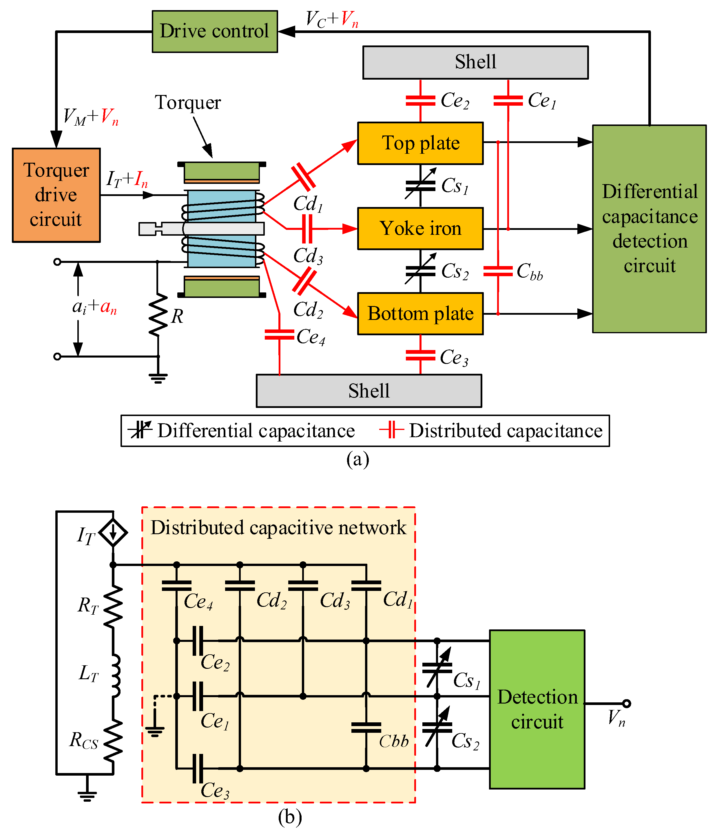
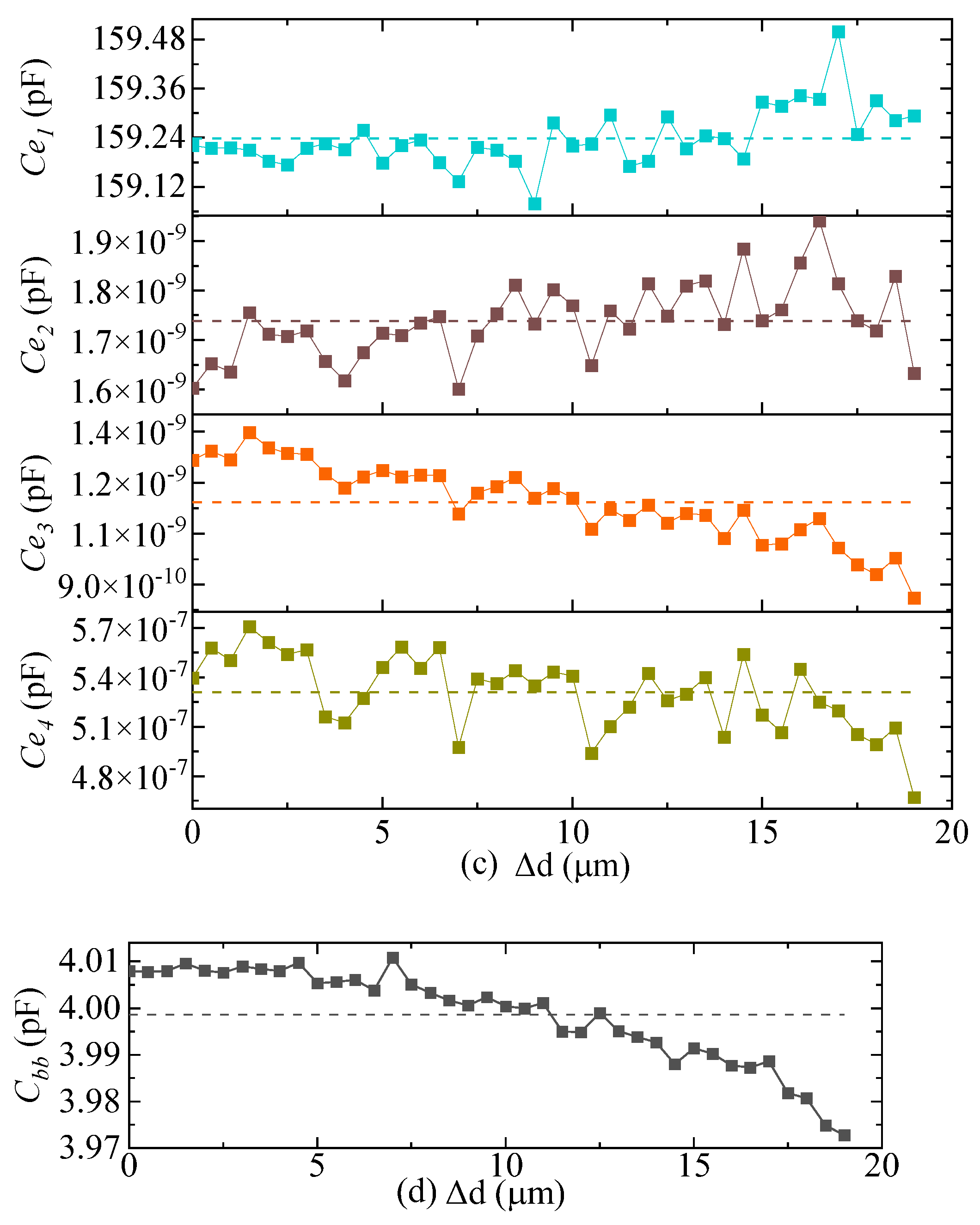
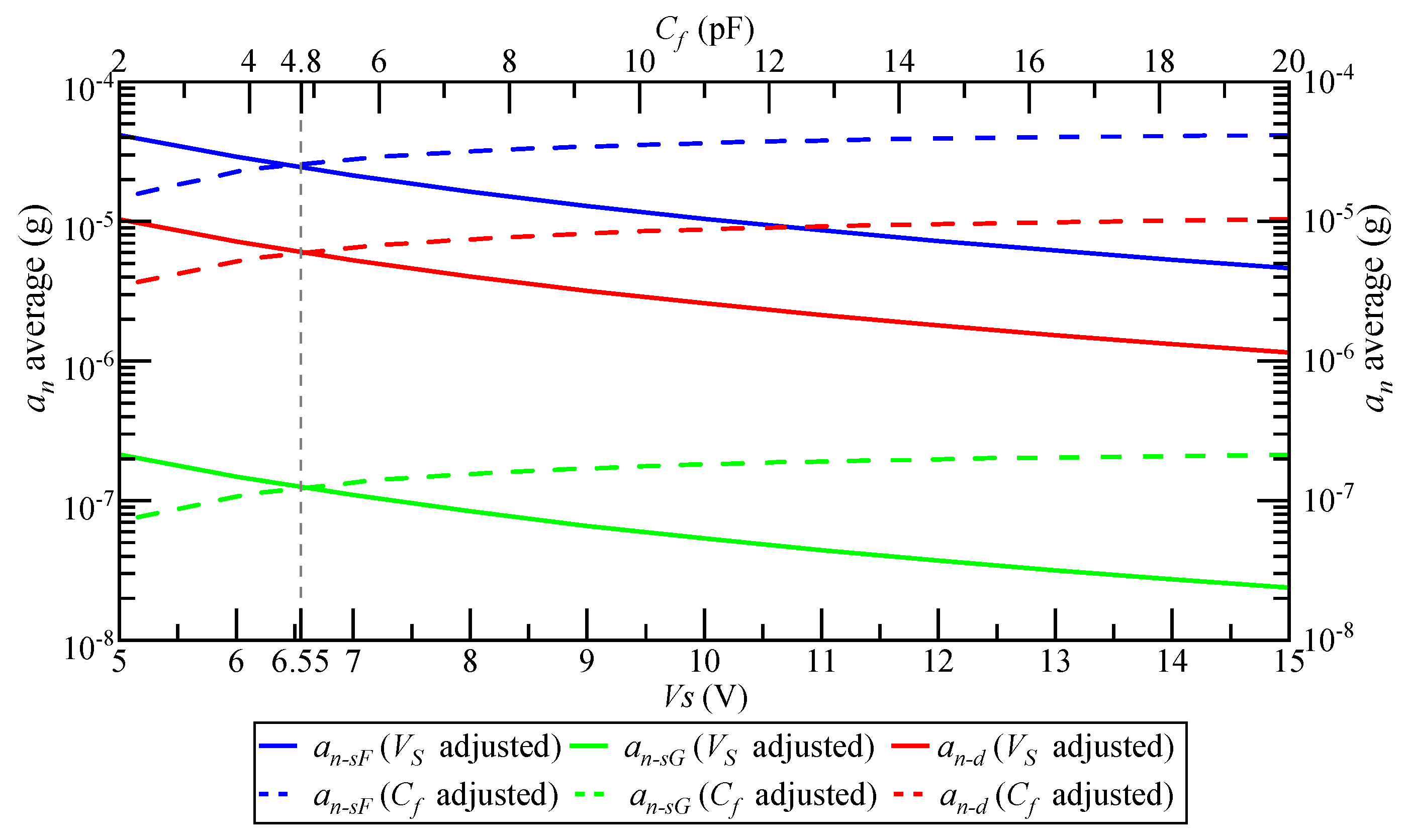
According to the equivalent circuit model of electric field coupling detection noise, the noise is related to the type of differential capacitance detection circuit. At present, the common differential capacitance detection circuits mainly include capacitance divider type, switch capacitance integral type, ring diode type and carrier modulation type detection circuits. Among them, the carrier modulation detection circuit is widely used in QFAs. The carrier modulation detection circuits are divided into single-channel carrier modulation (SCM) and dual-channel carrier modulation (DCM) detection circuits. In addition, the shell has two connection modes: grounded and float. Shell grounding is also a common electromagnetic shielding method. The float shell is designed to prevent the internal components from being destroyed in use. Different types of differential capacitance detection circuits and the connection mode of the accelerometer shell constitute multiple combinations of noise transfer paths.
3.1. Detection Noise Transfer System Structure of SCM Detection Circuit
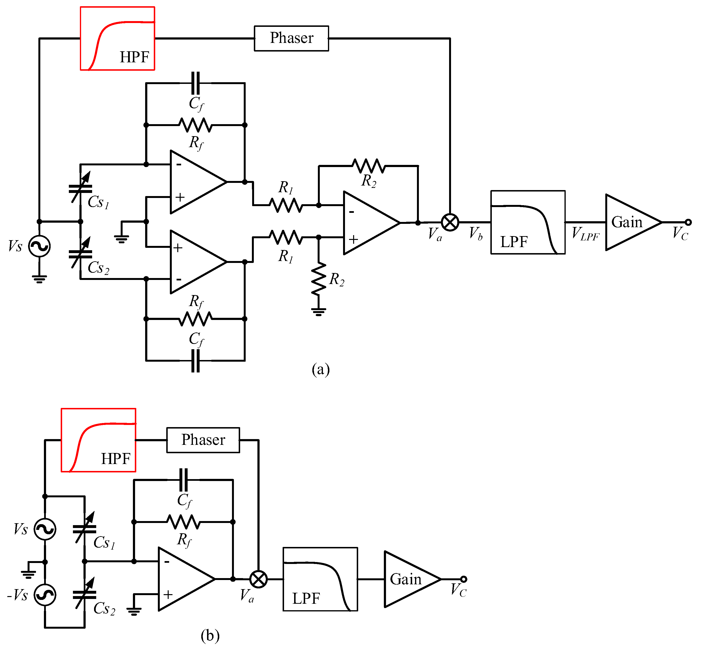
When an SCM detection circuit is used to detect differential capacitance, the structure of the detection circuit is as shown in
Figure 4a. The single-channel high-frequency sinusoidal carrier signal
is input to the differential capacitance fixed plate, and the signals of the two moving plates pass through the charge amplification circuit and the differential amplification circuit to obtain the modulated signal
, whose amplitude reflects the variation in the differential capacitance
.
The modulated signal
can be expressed as:
where
is the amplification factor of the differential amplifier circuit. Generally, the value of
ranges from dozens to hundreds of MΩ; thus, Equation (4) can be simplified as:
It is assumed that sin carrier signal
and differential capacitance variation
, where
and
are amplitude
and
, respectively;
is the frequency of carrier signal
, usually from tens of kHz to tens of MHz; and
is the effective detectable frequency of
, which is related to the bandwidth of the accelerometer closed-loop system, generally less than 1 kHz. We take the time-domain representation of
and
into Equation (5) to obtain:
The modulated signal
is mixed with the phase-adjusted carrier signal
through the mixer, and the mixing output signal
can be expressed as:
There are high-frequency signals of frequency
and low-frequency signals of the same frequency
in
. When
passes through a low-pass filter with a cut-off frequency of
, the high-frequency signals in
are filtered out, and only the low-frequency signals in the same frequency as
are retained. The filter output signal
can be expressed as:
After
adjusts the gain through the amplifier, the output voltage
of the SCM detection circuit is obtained:
where
is the amplification factor of the amplifier circuit. According to Equation (9), the output voltage
of the SCM detection circuit is directly proportional to the variation of differential capacitance
.
According to the equivalent circuit model of electric field coupling detection noise and the simulation results of distributed capacitance, the detection noise transfer path formed by the SCM detection circuit is as shown in
Figure 4b. After the voltage
on the torquer coil passes through the distributed capacitance network, it is loaded onto the three plates of the differential capacitor, and then passed into the charge amplification circuit and the differential amplification circuit to form a pseudo-modulated signal
. The signal loaded on the fixed plate is also passed into the phase-shift circuit as a pseudo-carrier signal
. After mixing
with
, the electric field coupling detection noise
is formed through a low-pass filter and gain-adjustment circuit. In the SCM detection noise transfer path,
forms a common-mode signal when it is transmitted to the detection circuit through
and
, which is cancelled when it goes through differential amplification, and does not affect the differential capacitance detection.
does not divide voltage or affect differential capacitance detection. We remove
,
, and
to obtain a simplified detection noise transfer path of the SCM detection circuit, as shown in
Figure 4c. In the transfer path of the detection noise of the SCM detection circuit, the distributed capacitance
between the torquer coil and the yoke iron and
between the yoke iron and the shell play a major role.
The process in which the torquer drive current
generates voltage
from the torquer coil can be expressed as:
where
is the frequency of the torquer drive current
. When the accelerometer float shell is used, the pseudo-carrier signal
can be expressed as:
The pseudo-modulated signal
can be expressed as:
In Equation (12),
can be ignored, and
can be expressed as:
When the shell is grounded, the pseudo-carrier signal
can be expressed as:
The pseudo-modulated signal
can be expressed as:
The accelerometer closed-loop system is linear;
,
, and
have the same frequency; and the maximum frequency is equal to the closed-loop system bandwidth.
and
multiply to produce a double-frequency effect, so that the frequency of
is twice that of
, and then through the mixing step, the output-signal frequency is three times that of
. Generally, the cut-off frequency of the low-pass filter circuit of the carrier modulation detection circuit is several times that of the closed-loop system bandwidth; therefore, the attenuation of the frequency-doubling signal through the filter circuit can be ignored. The structure of the detection noise transfer system of the SCM detection circuit is as shown in
Figure 4d. The detection noise
of SCM detection circuit can be expressed as:
where
represents the transfer process from
to carrier signal
,
when the float shell is used, and
when the shell is grounded;
represents the transfer process from the product of
and
to
.
when the float shell is used, and
when the shell is grounded.
3.2. Detection Noise Transfer System Structure of DCM Detection Circuit
When a DCM detection circuit is used to detect differential capacitance, the structure of the detection circuit is as shown in
Figure 5a.
and
are high-frequency sinusoidal carrier signals with the same frequency and amplitude and opposite phase, which are separately input to the two movable plates of the differential capacitor. After the output signals of the movable plate pass through the charge amplifier circuit, the modulated signal
can be expressed as:
As with the SCM detection circuit, after mixing, filtering, and gain adjustment of the modulated signal
are performed, a voltage signal
proportional to the change in differential capacitance
can be obtained, and expressed as:
The detection noise transfer path formed by the DCM detection circuit is shown in
Figure 5b. After the voltage
on the torquer coil passes through the distributed capacitance network, it is loaded onto the three plates of the differential capacitor, and then passed into the charge amplification circuit to form a pseudo-modulated signal
. The signal loaded on the top plate is also passed into the phase-shift circuit as a pseudo-carrier signal
. After mixing
with
, the electric field coupling detection noise
is formed through a low-pass filter and gain adjustment circuit. In the DCM detection noise transfer path,
is connected to the reverse port of the operational amplifier, which is approximately grounded and does not affect the differential capacitance detection.
does not divide the voltage or affect differential capacitance detection. We remove
and
to obtain a simplified detection noise transfer path of the DCM detection circuit, as shown in
Figure 5c. In the transfer path of the detection noise of the DCM detection circuit, the distributed capacitances
,
, and
between the torquer coil and the three plates of the differential capacitor play a major role.
The pseudo-carrier signal
can be expressed as
The equivalent capacitance
of the capacitance network composed of distributed capacitances
,
, and
and differential capacitors
and
can be expressed as
The pseudo-modulated signal
can be expressed as
The frequency of
and
is the same, and the frequency of the mixing output signal
is twice that of
. The structure of the detection noise transfer system of the DCM detection circuit is shown in
Figure 5d. The detection noise
of the DCM detection circuit can be expressed as:
where
represents the transfer process from
to carrier signal
, and
represents the transfer process from
to
.


