
A Thermoelectric Polymer Field-Effect Transistor via Iodine-Doped P3HT


Abstract
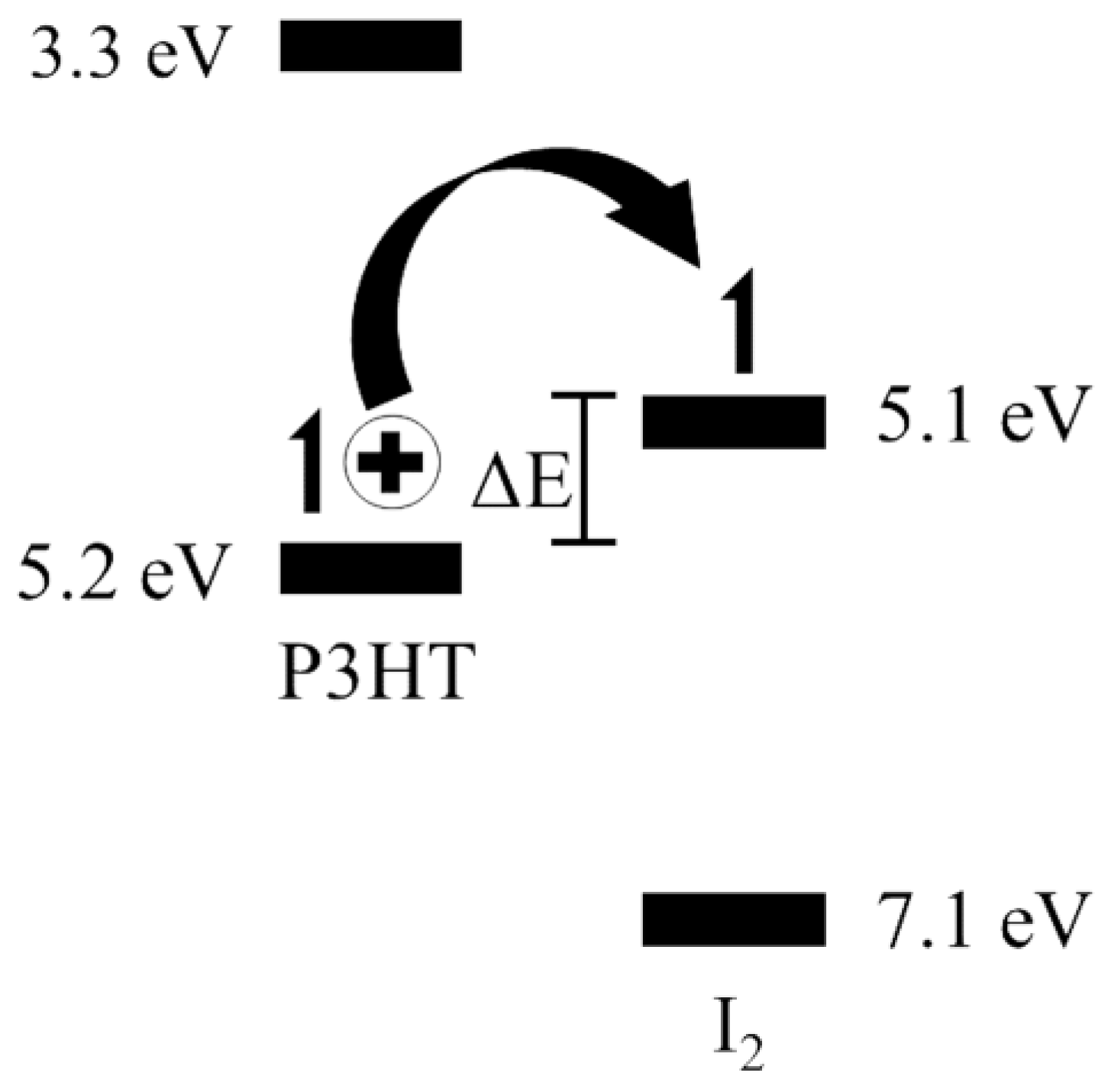
:1. Introduction
2. Experimental
2.1. Materials
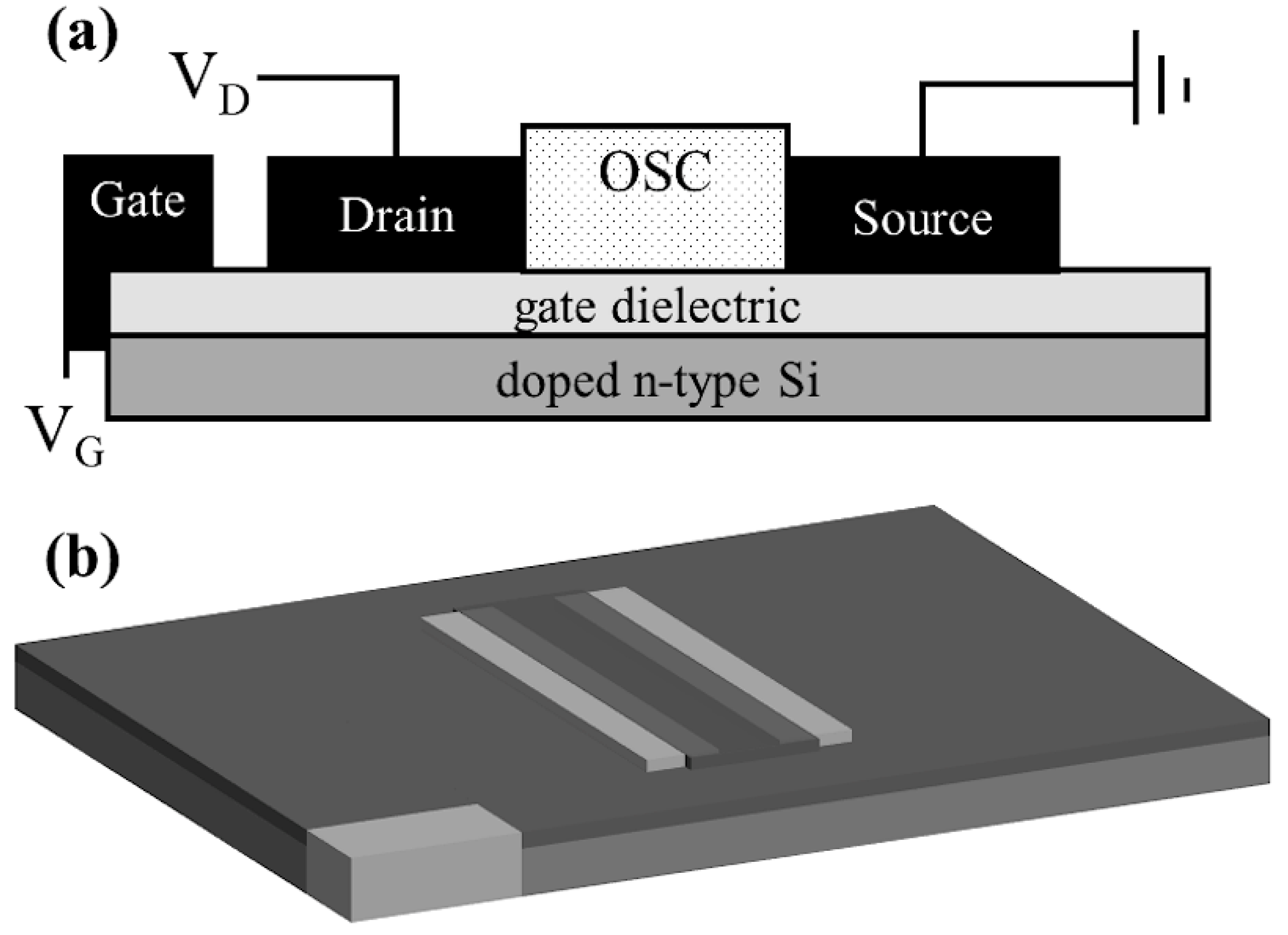
2.2. Solution and Device Fabrication
2.3. Field Effect and Seebeck Coefficient Characterizations
2.4. Atomic Force Microscopy
3. Results and Discussion
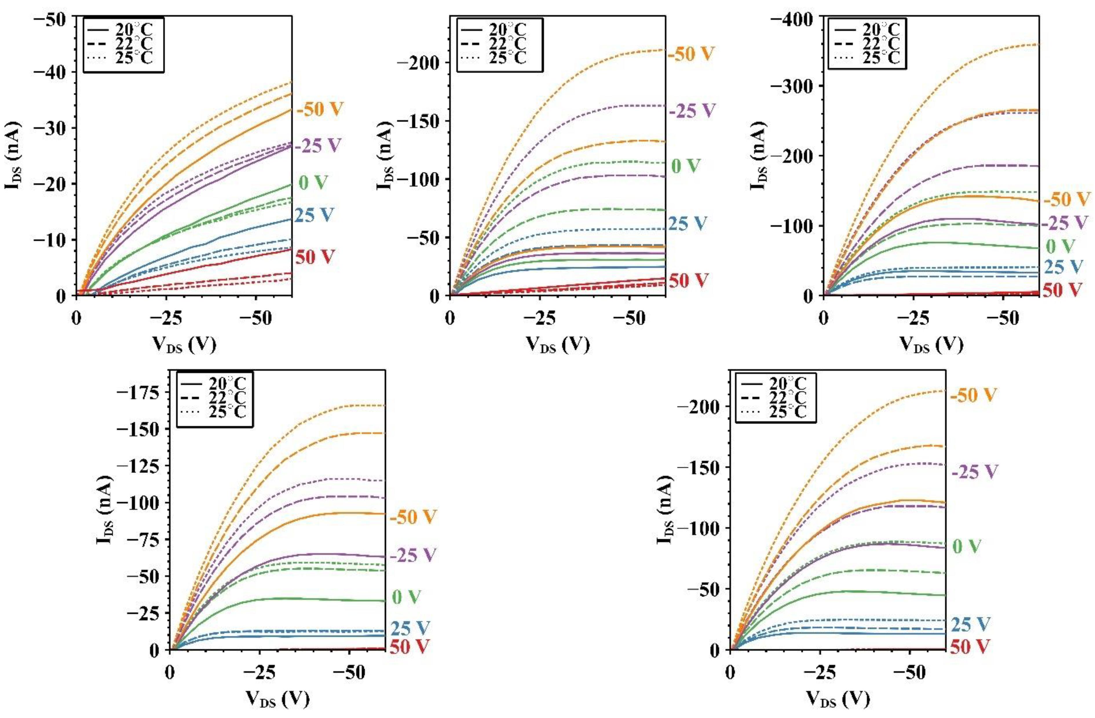
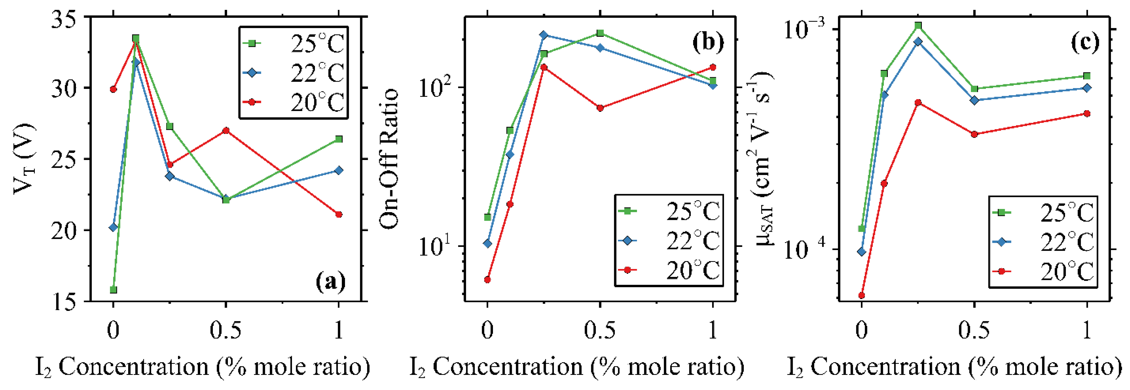
3.1. Optimization of Doping Concentration Range
3.2. Temperature Modulation of the Dual-Modulation OFET
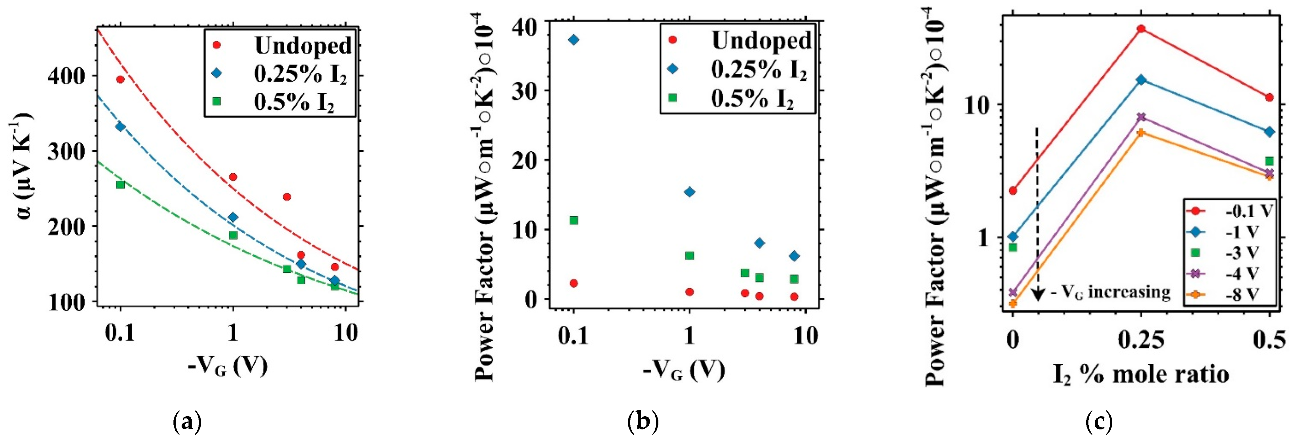
3.3. Gate Voltage Modulation of the Thermoelectric Properties
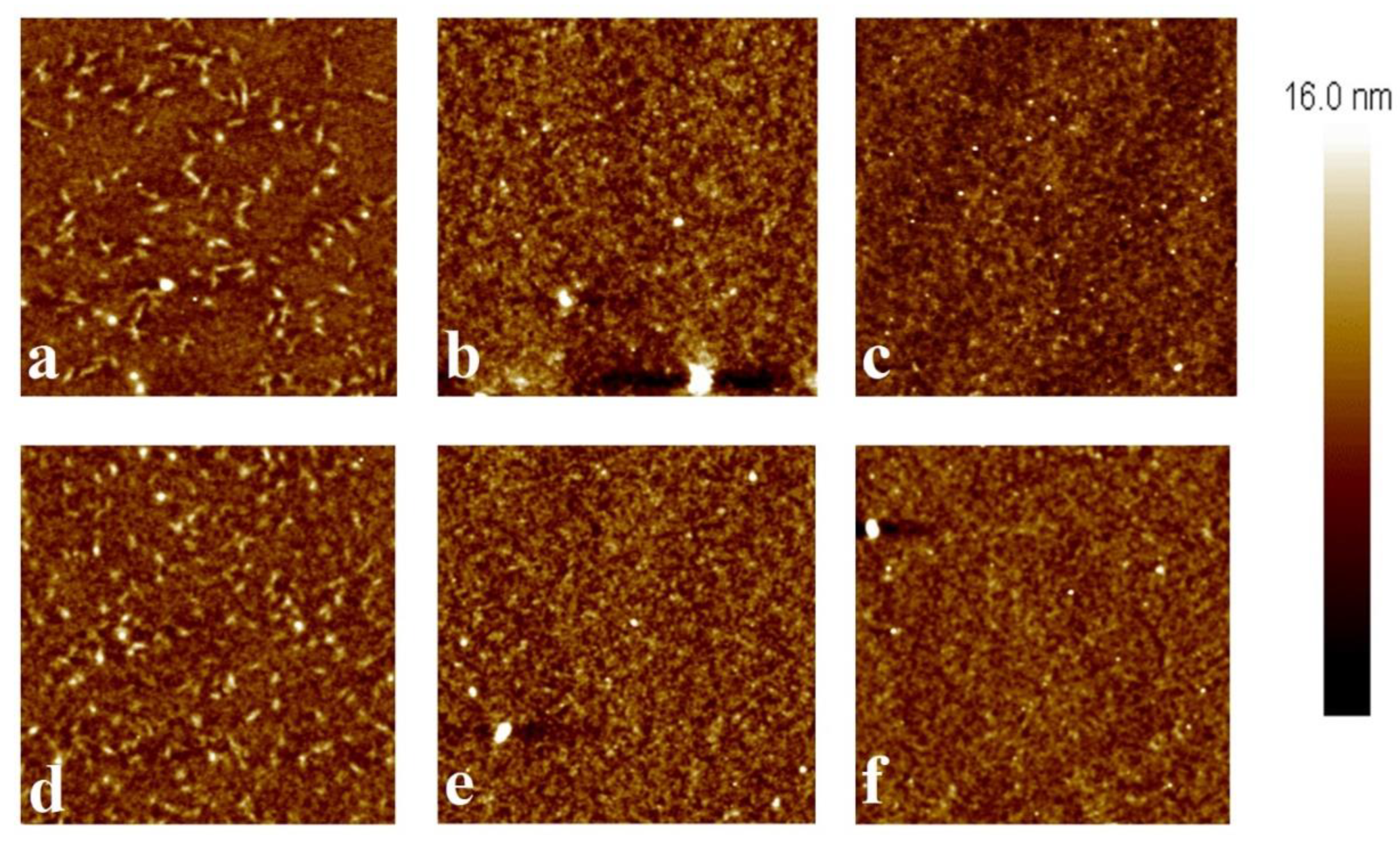
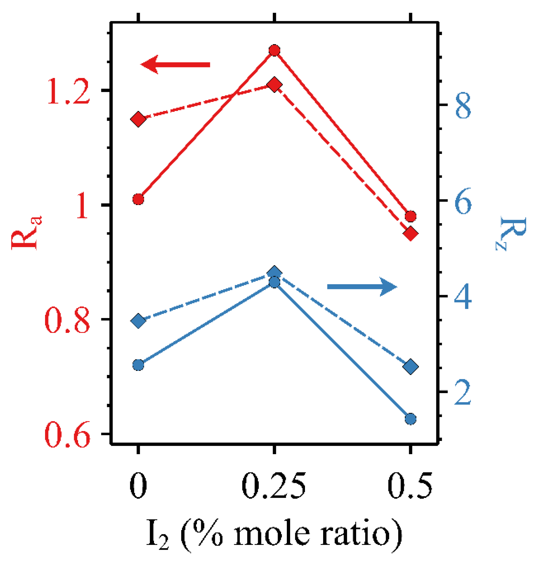
3.4. Atomic Force Microscopy
4. Conclusions
Author Contributions
Funding
Data Availability Statement
Acknowledgments
Conflicts of Interest
References
- Huewe, F.; Steeger, A.; Pflaum, J.; Kostova, K.; Dimitrov, V.; Burroughs, L.; Woodward, S.; Bauer, I.; Strohriegl, P. Low-cost and sustainable organic thermoelectrics based on low-dimensional molecular metals. Adv. Mater. 2017, 29, 1605682. [Google Scholar] [CrossRef] [PubMed]
- Kwon, S.; Kang, H.; Lee, J.; Lee, J.; Hong, S.; Kim, H.; Lee, K. Effect of processing additives on organic photovoltaics: Recent progress and future prospects. Adv. Energy Mater. 2016, 7, 1601496. [Google Scholar] [CrossRef]
- Richardson, B.J.; Zhu, L.; Yu, Q. Design and development of plasmonic nanostructured electrodes for ITO-free organic photovoltaic cells on rigid and highly flexible substrates. Nanotechnology 2017, 28, 165401. [Google Scholar] [CrossRef] [PubMed]
- Välimäki, M.; Jansson, E.; Korhonen, P.; Peltoniemi, A.; Rousu, S. Custom-Shaped Organic Photovoltaic Modules—Freedom of Design by Printing. Nanoscale Res. Lett. 2017, 12, 117. [Google Scholar] [CrossRef] [PubMed]
- Park, T.; Park, C.; Kim, B.; Shin, H.; Kim, E. Flexible PEDOT electrodes with large thermoelectric power factors to generate electricity by the touch of fingertips. Energy Environ. Sci. 2013, 6, 788–792. [Google Scholar] [CrossRef]
- Zhang, Q.; Sun, Y.; Xu, W.; Zhu, D. Thermoelectric energy from flexible P3HT films doped with a ferric salt of triflimide anions. Energy Environ. Sci. 2012, 5, 9639–9644. [Google Scholar] [CrossRef]
- Prabavathy, N.; Shalini, S.; Balasundaraprabhu, R.; Velauthapillai, D.; Prasanna, S.; Muthukumarasamy, N. Enhancement in the photostability of natural dyes for dye-sensitized solar cell (DSSC) applications: A review. Int. J. Energy Res. 2017, 41, 1372–1396. [Google Scholar] [CrossRef]
- Lucera, L.; Machui, F.; Schmidt, H.; Ahmad, T.; Kubis, P.; Strohm, S.; Hepp, J.; Vetter, A.; Egelhaaf, H.-J.; Brabec, C. Printed semi-transparent large area organic photovoltaic modules with power conversion efficiencies of close to 5%. Org. Electron. 2017, 45, 209–214. [Google Scholar] [CrossRef]
- Berny, S.; Krompiec, M.; Lozman, O.R.; Morse, G.E.; Nanson, L.; Pron, A.; Seidler, N.; Tiwana, P.; Blouin, N.; Lohr, A.; et al. Solar trees: First large-scale demonstration of fully solution coated, semitransparent, flexible organic photovoltaic modules. Adv. Sci. 2016, 3, 1500342. [Google Scholar] [CrossRef]
- Kim, H.; Lee, J.; Sohn, S.; Jung, D. Low-Temperature Process for Atomic Layer Chemical Vapor Deposition of an Al2O3 Passivation Layer for Organic Photovoltaic Cells. J. Nanosci. Nanotechnol. 2016, 16, 5285–5290. [Google Scholar] [CrossRef]
- Wu, X.; Mao, S.; Chen, J.; Huang, J. Strategies for Improving the Performance of Sensors Based on Organic Field-Effect Transistors. Adv. Mater. 2018, 30, e1705642. [Google Scholar] [CrossRef]
- Raval, H.N.; Rao, V.R. OFET Sensors with Poly 3-hexylthiophene and Pentacene as Channel Materials for Ionizing Radiation. MRS Proc. 2012, 1383, mrsf11. [Google Scholar] [CrossRef]
- Liu, S.; Al-Shadeedi, A.; Kaphle, V.; Lüssem, B. 67-1: Invited paper: Doped organic transistors—Increased stability and reproducibility for active matrix displays. SID Symp. Dig. Tech. Pap. 2018, 49, 884–887. [Google Scholar] [CrossRef]
- Sirringhaus, H.; Tessler, N.; Friend, R.H. Integrated optoelectronic devices based on conjugated polymers. Science 1998, 280, 1741–1744. [Google Scholar] [CrossRef] [PubMed]
- Xu, Y.; Sun, H.; Liu, A.; Zhu, H.; Li, W.; Lin, Y.; Noh, Y. Doping: A key enabler for organic transistors. Adv. Mater. 2018, 30, e1801830. [Google Scholar] [CrossRef] [PubMed]
- Wang, Z.; Zou, Y.; Chen, W.; Huang, Y.; Yao, C.; Zhang, Q. The role of weak molecular dopants in enhancing the performance of solution-processed organic field-effect transistors. Adv. Electron. Mater. 2018, 5, 1800547. [Google Scholar] [CrossRef]
- Hu, L.; Liu, T.; Duan, J.; Ma, X.; Ge, C.; Jiang, Y.; Qin, F.; Xiong, S.; Jiang, F.; Hu, B.; et al. An amidine-type n-dopant for solution-processed field-effect transistors and perovskite solar cells. Adv. Funct. Mater. 2017, 27, 1703254. [Google Scholar] [CrossRef]
- Ma, L.; Lee, W.H.; Park, Y.D.; Kim, J.S.; Lee, H.S.; Cho, K. High performance polythiophene thin-film transistors doped with very small amounts of an electron acceptor. Appl. Phys. Lett. 2008, 92, 063310. [Google Scholar] [CrossRef]
- Thomas, E.M.; Popere, B.C.; Fang, H.; Chabinyc, M.L.; Segalman, R.A. Role of disorder induced by doping on the thermoelectric properties of semiconducting polymers. Chem. Mater. 2018, 30, 2965–2972. [Google Scholar] [CrossRef]
- Venkateshvaran, D.; Kronemeijer, A.J.; Moriarty, J.; Emin, D.; Sirringhaus, H. Field-effect modulated Seebeck coefficient measurements in an organic polymer using a microfabricated on-chip architecture. APL Mater. 2014, 2, 032102. [Google Scholar] [CrossRef]
- Pernstich, K.P.; Rössner, B.; Batlogg, B. Field-effect-modulated Seebeck coefficient in organic semiconductors. Nat. Mater. 2008, 7, 321–325. [Google Scholar] [CrossRef] [PubMed]
- Warwick, C.N.; Venkateshvaran, D.; Sirringhaus, H. Accurate on-chip measurement of the Seebeck coefficient of high mobility small molecule organic semiconductors. APL Mater. 2015, 3, 096104. [Google Scholar] [CrossRef]
- Zhang, F.; Zang, Y.; Huang, D.; Di, C.; Gao, X.; Sirringhaus, H.; Zhu, D. Modulated thermoelectric properties of organic semiconductors using field-effect transistors. Adv. Funct. Mater. 2015, 25, 3004–3012. [Google Scholar] [CrossRef]
- Joseph, N. Demonstration of an Electro-Electric and Themo-Electric Dual Modulation Material and Device. Ph.D. Dissertation, Norfolk State University, Norfolk, VA, USA, 2021. [Google Scholar]
- Norman, J.W.; Lee, H.; Sun, S.-S. Polymer composites for potential thermo-electro dual sensors. In Proceedings of the Organic and Hybrid Sensors and Bioelectronics XII, San Diego, CA, USA, 11–13 August 2019; p. 1109608. [Google Scholar]
- Norman, J.W.; Sun, S.-S. A potential dual-functional thermoelectric and electroelectric polymer composite. Mater. Lett. 2022, 308, 131263. [Google Scholar] [CrossRef]
- Norman, J.; Sun, S. A Thermoelectric Polymer Field-effect Transistor via Iodine-doped P3HT. Preprints 2023, 2023121730. [Google Scholar] [CrossRef]
- Available online: https://en.wikipedia.org/wiki/Wearable_technology (accessed on 2 January 2024).
- Jiang, C.-X.; Cheng, X.-M.; Wu, X.-M.; Yang, X.-Y.; Yin, B.; Hua, Y.-L.; Wei, J.; Yin, S.-G. Effects of P3HT concentration on the performance of organic field effect transistors. Optoelectron. Lett. 2011, 7, 30–32. [Google Scholar] [CrossRef]
- Wang, X.; Ochiai, S.; Sawa, G.; Uchida, Y.; Kojima, K.; Ohashi, A.; Mizutani, T. Organic Field-Effect Transistors with Crosslinkable Poly(vinyl alcohol) Insulator and Spin-Coated/Drop-Cast Poly(3-hexylthiophene-2,5-diyl) Semiconductor. Jpn. J. Appl. Phys. 2007, 46, 1337. [Google Scholar] [CrossRef]
- Abbas, M.; Pivrikas, A.; Arici, E.; Tekin, N.; Ullah, M.; Sitter, H.; Sariciftci, N.S. Temperature dependent charge transport in organic field-effect transistors with the variation of both carrier concentration and electric field. J. Phys. D Appl. Phys. 2013, 46, 495105. [Google Scholar] [CrossRef]
- Horowitz, G.; Hajlaoui, R.; Delannoy, P. Temperature dependence of the field-effect mobility of Sexithiophene: Determination of the density of traps. J. Phys. III 1995, 5, 355–371. [Google Scholar] [CrossRef]
- Lee, H.O., III; Sun, S.-S. Properties and mechanisms of iodine doped of P3HT and P3HT/PCBM composites. AIMS Mater. Sci. 2018, 5, 479–493. [Google Scholar] [CrossRef]
- Sirringhaus, H.; Brown, P.J.; Friend, R.H.; Nielsen, M.M.; Bechgaard, K.; Langeveld-Voss, B.M.W.; Spiering, A.J.H.; Janssen, R.A.J.; Meijer, E.W.; Herwig, P.; et al. Two-dimensional charge transport in self-organized, high-mobility conjugated polymers. Nature 1999, 401, 685–688. [Google Scholar] [CrossRef]
- Kang, S.D.; Snyder, G.J. Charge-transport model for conducting polymers. Nat. Mater. 2016, 16, 252–257. [Google Scholar] [CrossRef] [PubMed]
- Zheng, J.-C. Recent advances on thermoelectric materials. Front. Phys. China 2008, 3, 269–279. [Google Scholar] [CrossRef]


| Doping (% Mole Ratio) | Sample Surface T (°C) | VT (V) | µSAT (cm2V−1s−1) | On/Off Ratio |
|---|---|---|---|---|
| Undoped | 20 | 57.6 | 5.13 × 10⁻⁵ | 1.01 × 101 |
| Undoped | 22 | 56.3 | 6.51 × 10⁻⁵ | 1.09 × 101 |
| Undoped | 25 | 55.3 | 6.40 × 10⁻⁵ | 1.25 × 101 |
| 0.25 | 20 | 68.0 | 9.28 × 10⁻⁴ | 1.66 × 101 |
| 0.25 | 22 | 76.3 | 9.14 × 10⁻⁴ | 3.38 × 101 |
| 0.25 | 25 | 74.3 | 1.01 × 10⁻³ | 3.91 × 101 |
| 0.5 | 20 | 58.2 | 5.91 × 10⁻⁴ | 3.70 × 101 |
| 0.5 | 22 | 59.3 | 6.51 × 10⁻⁴ | 3.73 × 101 |
| 0.5 | 25 | 60.5 | 7.04 × 10⁻⁴ | 3.61 × 101 |
Disclaimer/Publisher’s Note: The statements, opinions and data contained in all publications are solely those of the individual author(s) and contributor(s) and not of MDPI and/or the editor(s). MDPI and/or the editor(s) disclaim responsibility for any injury to people or property resulting from any ideas, methods, instructions or products referred to in the content. |
© 2024 by the authors. Licensee MDPI, Basel, Switzerland. This article is an open access article distributed under the terms and conditions of the Creative Commons Attribution (CC BY) license (https://creativecommons.org/licenses/by/4.0/).
Share and Cite
Norman, J.W.; Sun, S.-S. A Thermoelectric Polymer Field-Effect Transistor via Iodine-Doped P3HT. Micromachines 2024, 15, 172. https://doi.org/10.3390/mi15020172
Norman JW, Sun S-S. A Thermoelectric Polymer Field-Effect Transistor via Iodine-Doped P3HT. Micromachines. 2024; 15(2):172. https://doi.org/10.3390/mi15020172
Chicago/Turabian StyleNorman, Joseph Wayne, and Sam-Shajing Sun. 2024. "A Thermoelectric Polymer Field-Effect Transistor via Iodine-Doped P3HT" Micromachines 15, no. 2: 172. https://doi.org/10.3390/mi15020172