Next Issue
Volume 15, March
Previous Issue
Volume 15, January


Micromachines, Volume 15, Issue 2 (February 2024) – 124 articles

Cover Story (view full-size image): 
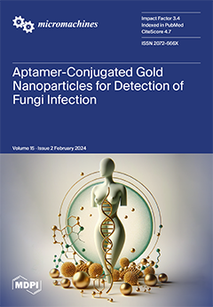
Candida albicans’ infection presents a global health and economic challenge, afflicting women with discomfort, mental distress, and fatalities in immunocompromised individuals. Current detection methods, relying on microscopy, culturing, or DNA amplification are prohibitively expensive, slow, and inaccessible in remote areas. Our study unveils an affordable, rapid detection platform. Leveraging aptamers for their selective recognition of 1,3-β-D glucan molecules, a hallmark of C. albicans cell walls, we employ aptamer-tagged gold core–shell nanoparticles. In the presence of a pathogen, these nanoparticles aggregate, causing a distinctive blue colour perceptible to the naked eye. This innovation holds the potential to transform Candida albicans diagnostics, particularly in underserved regions, thereby advancing women's healthcare. View this paper
  • Issues are regarded as officially published after their release is announced to the table of contents alert mailing list.
  • You may sign up for e-mail alerts to receive table of contents of newly released issues.
  • PDF is the official format for papers published in both, html and pdf forms. To view the papers in pdf format, click on the "PDF Full-text" link, and use the free Adobe Reader to open them.
Order results
Result details
Section
Select all
Export citation of selected articles as:
16 pages, 9950 KiB  
Article
Measurement and Data Correction of Channel Sampling Timing Walk-Off of Photonic Analog-to-Digital Converter in Signal Recovery
by Junli Qi, Xin Chen, Meicheng Fu, Hongyu Zhang, Wenjun Yi, Hui Zhang, Xiaoming Wei, Bo Shi, Tengfei Xu, Dezhi Su, Weihua Wang and Xiujian Li
Micromachines 2024, 15(2), 290; https://doi.org/10.3390/mi15020290 - 19 Feb 2024
Cited by 1 | Viewed by 709
Abstract
A two-channel, time–wavelength interleaved photonic analog-to-digital converter (PADC) system with a sampling rate of 10.4 GSa/s was established, and a concise method for measuring and data correcting the channel sampling timing walk-off of PADCs for signal recovery was proposed. The measurements show that [...] Read more.
A two-channel, time–wavelength interleaved photonic analog-to-digital converter (PADC) system with a sampling rate of 10.4 GSa/s was established, and a concise method for measuring and data correcting the channel sampling timing walk-off of PADCs for signal recovery was proposed. The measurements show that for the two RF signals of f1 = 100 MHz and f2 = 200 MHz, the channel sampling timing walk-off was 12 sampling periods, which results in an ENOB = −0.1051 bits for the 100 MHz directly synthesized signal, while the ENOB improved up to 4.0136 bits using shift synthesis. In addition, the peak limit method (PLM) and normalization processing were introduced to reduce the impacts of signal peak jitter and power inconsistency between two channels, which further improve the ENOB of the 100 MHz signal up to 4.5668 bits. All signals were analyzed and discussed in both time and frequency domains. The 21.1 GHz signal was also collected and converted using the established two-channel PADC system with the data correction method, combining the PLM, normalization, and shift synthesis, showing that the ENOB increased from the initial −0.9181 to 4.1913 bits, which demonstrates that our method can be effectively used for signal recovery in channel-interleaved PADCs. Full article
(This article belongs to the Section A:Physics)
Show Figures

Figure 1

12 pages, 3206 KiB  
Article
Mask-Moving-Lithography-Based High-Precision Surface Fabrication Method for Microlens Arrays
by Jianwen Gong, Ji Zhou, Junbo Liu, Song Hu, Jian Wang and Haifeng Sun
Micromachines 2024, 15(2), 289; https://doi.org/10.3390/mi15020289 - 19 Feb 2024
Viewed by 746
Abstract
Microlens arrays, as typical micro-optical elements, effectively enhance the integration and performance of optical systems. The surface shape errors and surface roughness of microlens arrays are the main indicators of their optical characteristics and determine their optical performance. In this study, a mask-moving-projection-lithography-based [...] Read more.
Microlens arrays, as typical micro-optical elements, effectively enhance the integration and performance of optical systems. The surface shape errors and surface roughness of microlens arrays are the main indicators of their optical characteristics and determine their optical performance. In this study, a mask-moving-projection-lithography-based high-precision surface fabrication method for microlens arrays is proposed, which effectively reduces the surface shape errors and surface roughness of microlens arrays. The pre-exposure technology is used to reduce the development threshold of the photoresist, thus eliminating the impact of the exposure threshold on the surface shape of the microlens. After development, the inverted air bath reflux method is used to bring the microlens array surface to a molten state, effectively eliminating surface protrusions. Experimental results show that the microlens arrays fabricated using this method had a root mean square error of less than 2.8%, and their surface roughness could reach the nanometer level, which effectively improves the fabrication precision for microlens arrays. Full article
Show Figures

Figure 1

15 pages, 2958 KiB  
Article
Biocatalytic Performance of β-Glucosidase Immobilized on 3D-Printed Single- and Multi-Channel Polylactic Acid Microreactors
by Andreas-Georgios Vasios, Anastasia Skonta, Michaela Patila and Haralambos Stamatis
Micromachines 2024, 15(2), 288; https://doi.org/10.3390/mi15020288 - 18 Feb 2024
Viewed by 916
Abstract
Microfluidic devices have attracted much attention in the current day owing to the unique advantages they provide. However, their application for industrial use is limited due to manufacturing limitations and high cost. Moreover, the scaling-up process of the microreactor has proven to be [...] Read more.
Microfluidic devices have attracted much attention in the current day owing to the unique advantages they provide. However, their application for industrial use is limited due to manufacturing limitations and high cost. Moreover, the scaling-up process of the microreactor has proven to be difficult. Three-dimensional (3D) printing technology is a promising solution for the above obstacles due to its ability to fabricate complex structures quickly and at a relatively low cost. Hence, combining the advantages of the microscale with 3D printing technology could enhance the applicability of microfluidic devices in the industrial sector. In the present work, a 3D-printed single-channel immobilized enzyme microreactor with a volume capacity of 30 μL was designed and created in one step via the fused deposition modeling (FDM) printing technique, using polylactic acid (PLA) as the printing material. The microreactor underwent surface modification with chitosan, and β-glucosidase from Thermotoga maritima was covalently immobilized. The immobilized biocatalyst retained almost 100% of its initial activity after incubation at different temperatures, while it could be effectively reused for up to 10 successful reaction cycles. Moreover, a multi-channel parallel microreactor incorporating 36 channels was developed, resulting in a significant increase in enzymatic productivity. Full article
(This article belongs to the Special Issue Microreactors and Their Applications)
Show Figures

Figure 1

18 pages, 4337 KiB  
Article
Magnetically Driven Biopsy Capsule Robot with Spring Mechanism
by Md Harun Or Rashid and Feng Lin
Micromachines 2024, 15(2), 287; https://doi.org/10.3390/mi15020287 - 18 Feb 2024
Viewed by 808
Abstract
In recent years, capsule endoscopes (CEs) have appeared as an advanced technology for the diagnosis of gastrointestinal diseases. However, only capturing the images limits the advanced diagnostic procedures and so on in CE’s applications. Herein, considering other extended functions like tissue sampling, a [...] Read more.
In recent years, capsule endoscopes (CEs) have appeared as an advanced technology for the diagnosis of gastrointestinal diseases. However, only capturing the images limits the advanced diagnostic procedures and so on in CE’s applications. Herein, considering other extended functions like tissue sampling, a novel wireless biopsy CE has been presented employing active locomotion. Two permanent magnets (PMs) have been placed into the robots, which control the actuation of the capsule robot (CR) and biopsy mechanism by employing an external electromagnetic actuation (EMA) system. A spring has been attached to the biopsy mechanism to retract the biopsy tool after tissue collection. A camera module has also been attached to the front side of the CR to detect the target point and observe the biopsy process on the lesion. A prototype of CR was fabricated with a diameter of 12 mm and a length of 32 mm. A spring mechanism with a biopsy needle was placed inside the CR and sprang out around 5 mm. An in vitro experiment was conducted, which demonstrated the precise control translation (2 mm/s and 3 mm/s in the x and y directions, respectively) and desired extrusion of the biopsy mechanism (~5 mm) for sampling the tissue. A needle-based biopsy capsule robot (NBBCR) has been designed to perform the desired controlled locomotion and biopsy function by external force. This proposed active locomoted untethered NBBCR can be wirelessly controlled to perform extended function precisely, advancing the intestinal CE technique for clinical applications. Full article
Show Figures

Figure 1

15 pages, 2385 KiB  
Article
In Vivo Characterization of Intracortical Probes with Focused Ion Beam-Etched Nanopatterned Topographies
by Jonathan L. Duncan, Jaime J. Wang, Gabriele Glusauskas, Gwendolyn R. Weagraff, Yue Gao, George F. Hoeferlin, Allen H. Hunter, Allison Hess-Dunning, Evon S. Ereifej and Jeffrey R. Capadona
Micromachines 2024, 15(2), 286; https://doi.org/10.3390/mi15020286 - 17 Feb 2024
Viewed by 835
Abstract
(1) Background: Intracortical microelectrodes (IMEs) are an important part of interfacing with the central nervous system (CNS) and recording neural signals. However, recording electrodes have shown a characteristic steady decline in recording performance owing to chronic neuroinflammation. The topography of implanted devices has [...] Read more.
(1) Background: Intracortical microelectrodes (IMEs) are an important part of interfacing with the central nervous system (CNS) and recording neural signals. However, recording electrodes have shown a characteristic steady decline in recording performance owing to chronic neuroinflammation. The topography of implanted devices has been explored to mimic the nanoscale three-dimensional architecture of the extracellular matrix. Our previous work used histology to study the implant sites of non-recording probes and showed that a nanoscale topography at the probe surface mitigated the neuroinflammatory response compared to probes with smooth surfaces. Here, we hypothesized that the improvement in the neuroinflammatory response for probes with nanoscale surface topography would extend to improved recording performance. (2) Methods: A novel design modification was implemented on planar silicon-based neural probes by etching nanopatterned grooves (with a 500 nm pitch) into the probe shank. To assess the hypothesis, two groups of rats were implanted with either nanopatterned (n = 6) or smooth control (n = 6) probes, and their recording performance was evaluated over 4 weeks. Postmortem gene expression analysis was performed to compare the neuroinflammatory response from the two groups. (3) Results: Nanopatterned probes demonstrated an increased impedance and noise floor compared to controls. However, the recording performances of the nanopatterned and smooth probes were similar, with active electrode yields for control probes and nanopatterned probes being approximately 50% and 45%, respectively, by 4 weeks post-implantation. Gene expression analysis showed one gene, Sirt1, differentially expressed out of 152 in the panel. (4) Conclusions: this study provides a foundation for investigating novel nanoscale topographies on neural probes. Full article
(This article belongs to the Special Issue Bioinspired Materials and Microdevices: Fabrications and Applications)
Show Figures

Figure 1

12 pages, 8869 KiB  
Article
Hydrophobic Surface Array Structure Based on Laser-Induced Graphene for Deicing and Anti-Icing Applications
by Mian Zhong, Shichen Li, Yao Zou, Hongyun Fan, Yong Jiang, Chao Qiu, Jinling Luo and Liang Yang
Micromachines 2024, 15(2), 285; https://doi.org/10.3390/mi15020285 - 17 Feb 2024
Cited by 8 | Viewed by 833
Abstract
The exceptional performance of graphene has driven the advancement of its preparation techniques and applications. Laser-induced graphene (LIG), as a novel graphene preparation technique, has been applied in various fields. Graphene periodic structures created by the LIG technique exhibit superhydrophobic characteristics and can [...] Read more.
The exceptional performance of graphene has driven the advancement of its preparation techniques and applications. Laser-induced graphene (LIG), as a novel graphene preparation technique, has been applied in various fields. Graphene periodic structures created by the LIG technique exhibit superhydrophobic characteristics and can be used for deicing and anti-icing applications, which are significantly influenced by the laser parameters. The laser surface treatment process was simulated by a finite element software analysis (COMSOL Multiphysics) to optimize the scanning parameter range, and the linear array surface structure was subsequently fabricated by the LIG technique. The generation of graphene was confirmed by Raman spectroscopy and energy-dispersive X-ray spectroscopy. The periodic linear array structure was observed by scanning electron microscopy (SEM) and confocal laser imaging (CLSM). In addition, CLSM testings, contact angle measurements, and delayed icing experiments were systematically performed to investigate the effect of scanning speed on surface hydrophobicity. The results show that high-quality and uniform graphene can be achieved using the laser scanning speed of 125 mm/s. The periodic linear array structures can obviously increase the contact angle and suppress delayed icing. Furthermore, these structures have the enhanced ability of the electric heating deicing, which can reach 100 °C and 240 °C within 15 s and within 60 s under the DC voltage power supply ranging from 3 to 7 V, respectively. These results indicate that the LIG technique can be developed to provide an efficient, economical, and convenient approach for preparing graphene and that the hydrophobic surface array structure based on LIG has considerable potential for deicing and anti-icing applications. Full article
(This article belongs to the Special Issue Optical and Laser Material Processing)
Show Figures

Figure 1

17 pages, 3795 KiB  
Article
Consideration of Power Transmission Characteristics in a Micro-Gear Train
by Yasuhiko Arai
Micromachines 2024, 15(2), 284; https://doi.org/10.3390/mi15020284 - 17 Feb 2024
Viewed by 772
Abstract
Characteristics related to power transmission in the micro-domain, based on dry rolling contact of the gears, were investigated using a 3D-printed gear train with a pitch circle diameter of 84 µm in order to experimentally compare the power transmission efficiency in the macro- [...] Read more.
Characteristics related to power transmission in the micro-domain, based on dry rolling contact of the gears, were investigated using a 3D-printed gear train with a pitch circle diameter of 84 µm in order to experimentally compare the power transmission efficiency in the macro- and micro-domains. For a basic gear train with two intermeshing gears, it was shown that the gear train in the micro-domain was capable of transmitting power to the same extent as in the macro-domain. However, in gear trains with complex power transmission paths, assuming a planetary gear train with multiple meshing gears, it has been shown that the power transmission characteristics of micro-domain gears differ from those in the macro-domain. The use of gear trains in the micro-region necessitates consideration of the loss of transmitted torque due to contact between tooth surfaces, which is unique to the micro-region and different from its use in the macro-region. Full article
(This article belongs to the Section E:Engineering and Technology)
Show Figures

Figure 1

0 pages, 3575 KiB  
Article
Comprehensive Noise Modeling of Piezoelectric Charge Accelerometer with Signal Conditioning Circuit
by Ghulam Ali and Faisal Mohd-Yasin
Micromachines 2024, 15(2), 283; https://doi.org/10.3390/mi15020283 - 17 Feb 2024
Viewed by 937
Abstract
This paper reports on noise modeling of a piezoelectric charge accelerometer with a signal conditioning circuit. The charge output is converted into voltage and amplified using a JFET operational amplifier that has high input resistance and low noise. The noise sources in the [...] Read more.
This paper reports on noise modeling of a piezoelectric charge accelerometer with a signal conditioning circuit. The charge output is converted into voltage and amplified using a JFET operational amplifier that has high input resistance and low noise. The noise sources in the whole system include electrical and mechanical thermal noises of the accelerometer, thermal noises of resistors, and voltage and current noises of the operational amplifier. Noise gain of each source is derived from small signal circuit analysis. It is found that the feedback resistor of the operational amplifier is a major source of noise in low frequencies, whereas electrical thermal noise of the accelerometer dominates the rest of spectrum. This method can be used to pair a highly sensitive sensor with a single JFET operational amplifier instead of a multi-stage signal conditioning circuit. Full article
(This article belongs to the Collection Piezoelectric Transducers: Materials, Devices and Applications)
Show Figures

Figure 1

43 pages, 19909 KiB  
Review
Confined Space Nanoarchitectonics for Dynamic Functions and Molecular Machines
by Katsuhiko Ariga
Micromachines 2024, 15(2), 282; https://doi.org/10.3390/mi15020282 - 17 Feb 2024
Viewed by 1634
Abstract
Nanotechnology has advanced the techniques for elucidating phenomena at the atomic, molecular, and nano-level. As a post nanotechnology concept, nanoarchitectonics has emerged to create functional materials from unit structures. Consider the material function when nanoarchitectonics enables the design of materials whose internal structure [...] Read more.
Nanotechnology has advanced the techniques for elucidating phenomena at the atomic, molecular, and nano-level. As a post nanotechnology concept, nanoarchitectonics has emerged to create functional materials from unit structures. Consider the material function when nanoarchitectonics enables the design of materials whose internal structure is controlled at the nanometer level. Material function is determined by two elements. These are the functional unit that forms the core of the function and the environment (matrix) that surrounds it. This review paper discusses the nanoarchitectonics of confined space, which is a field for controlling functional materials and molecular machines. The first few sections introduce some of the various dynamic functions in confined spaces, considering molecular space, materials space, and biospace. In the latter two sections, examples of research on the behavior of molecular machines, such as molecular motors, in confined spaces are discussed. In particular, surface space and internal nanospace are taken up as typical examples of confined space. What these examples show is that not only the central functional unit, but also the surrounding spatial configuration is necessary for higher functional expression. Nanoarchitectonics will play important roles in the architecture of such a total system. Full article
(This article belongs to the Special Issue Feature Papers of Micromachines in Chemistry 2023)
Show Figures

Figure 1

53 pages, 5520 KiB  
Review
An Overview of the Recent Advances in Pool Boiling Enhancement Materials, Structrure, and Devices
by José Pereira, Reinaldo Souza, Rui Lima, António Moreira and Ana Moita
Micromachines 2024, 15(2), 281; https://doi.org/10.3390/mi15020281 - 17 Feb 2024
Viewed by 985
Abstract
This review attempts to provide a comprehensive assessment of recent methodologies, structures, and devices for pool boiling heat transfer enhancement. Several enhancement approaches relating to the underlying fluid route and the capability to eliminate incipient boiling hysteresis, augment the nucleate boiling heat transfer [...] Read more.
This review attempts to provide a comprehensive assessment of recent methodologies, structures, and devices for pool boiling heat transfer enhancement. Several enhancement approaches relating to the underlying fluid route and the capability to eliminate incipient boiling hysteresis, augment the nucleate boiling heat transfer coefficient, and improve the critical heat flux are assessed. Hence, this study addresses the most relevant issues related to active and passive enhancement techniques and compound enhancement schemes. Passive heat transfer enhancement techniques encompass multiscale surface modification of the heating surface, such as modification with nanoparticles, tunnels, grooves, porous coatings, and enhanced nanostructured surfaces. Also, there are already studies on the employment of a wide range of passive enhancement techniques, like displaced enhancement, swirl flow aids, and bi-thermally conductive surfaces. Moreover, the combined usage of two or more enhancement techniques, commonly known as compound enhancement approaches, is also addressed in this survey. Additionally, the present work highlights the existing scarcity of sufficiently large available databases for a given enhancement methodology regarding the influencing factors derived from the implementation of innovative thermal management systems for temperature-sensitive electronic and power devices, for instance, material, morphology, relative positioning and orientation of the boiling surface, and nucleate boiling heat transfer enhancement pattern and scale. Such scarcity means the available findings are not totally accurate and suitable for the design and implementation of new thermal management systems. The analysis of more than 100 studies in this field shows that all such improvement methodologies aim to enhance the nucleate boiling heat transfer parameters of the critical heat flux and nucleate heat transfer coefficient in pool boiling scenarios. Finally, diverse challenges and prospects for further studies are also pointed out, aimed at developing important in-depth knowledge of the underlying enhancement mechanisms of such techniques. Full article
(This article belongs to the Special Issue Feature Reviews in Micromachines 2023)
Show Figures

Figure 1

13 pages, 4453 KiB  
Article
Using Compound Neural Action Potentials for Functional Validation of a High-Density Intraneural Interface: A Preliminary Study
by Aritra Kundu, Erin Patrick, Seth Currlin, Ryan Madler, Francisco Delgado, Ahmed Fahmy, Rik Verplancke, Marco Ballini, Dries Braeken, Maaike Op de Beeck, Nima Maghari, Kevin J. Otto and Rizwan Bashirullah
Micromachines 2024, 15(2), 280; https://doi.org/10.3390/mi15020280 - 17 Feb 2024
Viewed by 716
Abstract
Compound nerve action potentials (CNAPs) were used as a metric to assess the stimulation performance of a novel high-density, transverse, intrafascicular electrode in rat models. We show characteristic CNAPs recorded from distally implanted cuff electrodes. Evaluation of the CNAPs as a function of [...] Read more.
Compound nerve action potentials (CNAPs) were used as a metric to assess the stimulation performance of a novel high-density, transverse, intrafascicular electrode in rat models. We show characteristic CNAPs recorded from distally implanted cuff electrodes. Evaluation of the CNAPs as a function of stimulus current and calculation of recruitment plots were used to obtain a qualitative approximation of the neural interface’s placement and orientation inside the nerve. This method avoids elaborate surgeries required for the implantation of EMG electrodes and thus minimizes surgical complications and may accelerate the healing process of the implanted subject. Full article
(This article belongs to the Special Issue Progress and Challenges of Implantable Neural Interfaces)
Show Figures

Figure 1

15 pages, 4821 KiB  
Article
Investigation of New Accelerometer Based on Capacitive Micromachined Ultrasonic Transducer (CMUT) with Ring-Perforation Membrane
by Luhao Gou, Hongliang Wang, Qi Ding, Yulong Liu, Runze Yang, Feng Zhang, Pengcheng Zhang and Gang Cao
Micromachines 2024, 15(2), 279; https://doi.org/10.3390/mi15020279 - 16 Feb 2024
Viewed by 734
Abstract
Capacitive micromachined ultrasonic transducer (CMUT) has been widely studied due to its excellent resonance characteristics and array integration. This paper presents the first study of the CMUT electrostatic stiffness resonant accelerometer. To improve the sensitivity of the CMUT accelerometer, this paper innovatively proposes [...] Read more.
Capacitive micromachined ultrasonic transducer (CMUT) has been widely studied due to its excellent resonance characteristics and array integration. This paper presents the first study of the CMUT electrostatic stiffness resonant accelerometer. To improve the sensitivity of the CMUT accelerometer, this paper innovatively proposes the CMUT ring-perforation membrane structure, which effectively improves the acceleration sensitivity by reducing the mechanical stiffness of the elastic membrane. The acceleration sensitivity is 10.9 (Hz/g) in the acceleration range of 0–20 g, which is 100% higher than that of the conventional CMUT structure. This research contributes to the acceleration measurement field of CMUT and can effectively contribute to the breakthrough of vibration acceleration monitoring technology in aerospace, medical equipment, and automotive electronics. Full article
Show Figures

Figure 1

17 pages, 18140 KiB  
Article
Influence of Process Energy on the Formation of Imperfections in Body-Centered Cubic Cells with Struts in the Vertical Orientation Produced by Laser Powder Bed Fusion from the Magnesium Alloy WE43
by Jan Jaroš, Ondřej Vaverka, Sascha Senck and Daniel Koutný
Micromachines 2024, 15(2), 278; https://doi.org/10.3390/mi15020278 - 15 Feb 2024
Viewed by 716
Abstract
The low specific density and good strength-to-weight ratio make magnesium alloys a promising material for lightweight applications. The combination of the properties of magnesium alloys and Additive Manufacturing by the Laser Powder Bed Fusion (LPBF) process enables the production of complex geometries such [...] Read more.
The low specific density and good strength-to-weight ratio make magnesium alloys a promising material for lightweight applications. The combination of the properties of magnesium alloys and Additive Manufacturing by the Laser Powder Bed Fusion (LPBF) process enables the production of complex geometries such as lattice or bionic structures. Magnesium structures are intended to drastically reduce the weight of components and enable a reduction in fuel consumption, particularly in the aerospace and automotive industries. However, the LPBF processing of magnesium structures is a challenge. In order to produce high-quality structures, the process parameters must be developed in such a way that imperfections such as porosity, high surface roughness and dimensional inaccuracy are suppressed. In this study, the contour scanning strategy is used to produce vertical and inclined struts with diameters ranging from 0.5 to 3 mm. The combination of process parameters such as laser power, laser speed and overlap depend on the inclination and diameter of the strut. The process parameters with an area energy of 1.15–1.46 J/mm2 for struts with a diameter of 0.5 mm and an area energy of 1.62–3.69 J/mm2 for diameters of 1, 2 and 3 mm achieve a relative material density of 99.2 to 99.6%, measured on the metallographic sections. The results are verified by CT analyses of BCCZ cells, which achieve a relative material density of over 99.3%. The influence of the process parameters on the quality of struts is described and discussed. Full article
Show Figures

Figure 1

18 pages, 3877 KiB  
Article
Batch Fabrication of Microelectrode Arrays with Glassy Carbon Microelectrodes and Interconnections for Neurochemical Sensing: Promises and Challenges
by Emma-Bernadette A. Faul, Austin M. Broussard, Daniel R. Rivera, May Yoon Pwint, Bingchen Wu, Qun Cao, Davis Bailey, X. Tracy Cui and Elisa Castagnola
Micromachines 2024, 15(2), 277; https://doi.org/10.3390/mi15020277 - 15 Feb 2024
Viewed by 1108
Abstract
Flexible multielectrode arrays with glassy carbon (GC) electrodes and metal interconnection (hybrid MEAs) have shown promising performance in multi-channel neurochemical sensing. A primary challenge faced by hybrid MEAs fabrication is the adhesion of the metal traces with the GC electrodes, as prolonged [...] Read more.
Flexible multielectrode arrays with glassy carbon (GC) electrodes and metal interconnection (hybrid MEAs) have shown promising performance in multi-channel neurochemical sensing. A primary challenge faced by hybrid MEAs fabrication is the adhesion of the metal traces with the GC electrodes, as prolonged electrical and mechanical stimulation can lead to adhesion failure. Previous devices with GC electrodes and interconnects made of a homogeneous material (all GC) demonstrated exceptional electrochemical stability but required miniaturization for enhanced tissue integration and chronic electrochemical sensing. In this study, we used two different methods for the fabrication of all GC-MEAs on thin flexible substrates with miniaturized features. The first method, like that previously reported, involves a double pattern-transfer photolithographic process, including transfer-bonding on temporary polymeric support. The second method requires a double-etching process, which uses a 2 µm-thick low stress silicon nitride coating of the Si wafer as the bottom insulator layer for the MEAs, bypassing the pattern-transfer and demonstrating a novel technique with potential advantages. We confirmed the feasibility of the two fabrication processes by verifying the practical conductivity of 3 µm-wide 2 µm-thick GC traces, the GC microelectrode functionality, and their sensing capability for the detection of serotonin using fast scan cyclic voltammetry. Through the exchange and discussion of insights regarding the strengths and limitations of these microfabrication methods, our goal is to propel the advancement of GC-based MEAs for the next generation of neural interface devices. Full article
(This article belongs to the Special Issue Biosensors for Biomedical and Environmental Applications, Volume 2)
Show Figures

Figure 1

22 pages, 13911 KiB  
Article
Stereo Visual Servoing Control of a Soft Endoscope for Upper Gastrointestinal Endoscopic Submucosal Dissection
by Jian Chen, Shuai Wang, Qingxiang Zhao, Wei Huang, Mingcong Chen, Jian Hu, Yihe Wang and Hongbin Liu
Micromachines 2024, 15(2), 276; https://doi.org/10.3390/mi15020276 - 15 Feb 2024
Viewed by 852
Abstract
Quickly and accurately completing endoscopic submucosal dissection (ESD) operations within narrow lumens is currently challenging because of the environment’s high flexibility, invisible collision, and natural tissue motion. This paper proposes a novel stereo visual servoing control for a dual-segment robotic endoscope (DSRE) for [...] Read more.
Quickly and accurately completing endoscopic submucosal dissection (ESD) operations within narrow lumens is currently challenging because of the environment’s high flexibility, invisible collision, and natural tissue motion. This paper proposes a novel stereo visual servoing control for a dual-segment robotic endoscope (DSRE) for ESD surgery. Departing from conventional monocular-based methods, our DSRE leverages stereoscopic imaging to rapidly extract precise depth data, enabling quicker controller convergence and enhanced surgical accuracy. The system’s dual-segment configuration enables agile maneuverability around lesions, while its compliant structure ensures adaptability within the surgical environment. The implemented stereo visual servo controller uses image features for real-time feedback and dynamically updates gain coefficients, facilitating rapid convergence to the target. In visual servoing experiments, the controller demonstrated strong performance across various tasks. Even when subjected to unknown external forces, the controller maintained robust performance in target tracking. The feasibility and effectiveness of the DSRE were further verified through ex vivo experiments. We posit that this novel system holds significant potential for clinical application in ESD surgeries. Full article
Show Figures

Figure 1

35 pages, 5321 KiB  
Review
Evolution of the Microrobots: Stimuli-Responsive Materials and Additive Manufacturing Technologies Turn Small Structures into Microscale Robots
by Frank Marco den Hoed, Marco Carlotti, Stefano Palagi, Patrizio Raffa and Virgilio Mattoli
Micromachines 2024, 15(2), 275; https://doi.org/10.3390/mi15020275 - 15 Feb 2024
Viewed by 1536
Abstract
The development of functional microsystems and microrobots that have characterized the last decade is the result of a synergistic and effective interaction between the progress of fabrication techniques and the increased availability of smart and responsive materials to be employed in the latter. [...] Read more.
The development of functional microsystems and microrobots that have characterized the last decade is the result of a synergistic and effective interaction between the progress of fabrication techniques and the increased availability of smart and responsive materials to be employed in the latter. Functional structures on the microscale have been relevant for a vast plethora of technologies that find application in different sectors including automotive, sensing devices, and consumer electronics, but are now also entering medical clinics. Working on or inside the human body requires increasing complexity and functionality on an ever-smaller scale, which is becoming possible as a result of emerging technology and smart materials over the past decades. In recent years, additive manufacturing has risen to the forefront of this evolution as the most prominent method to fabricate complex 3D structures. In this review, we discuss the rapid 3D manufacturing techniques that have emerged and how they have enabled a great leap in microrobotic applications. The arrival of smart materials with inherent functionalities has propelled microrobots to great complexity and complex applications. We focus on which materials are important for actuation and what the possibilities are for supplying the required energy. Furthermore, we provide an updated view of a new generation of microrobots in terms of both materials and fabrication technology. While two-photon lithography may be the state-of-the-art technology at the moment, in terms of resolution and design freedom, new methods such as two-step are on the horizon. In the more distant future, innovations like molecular motors could make microscale robots redundant and bring about nanofabrication. Full article
(This article belongs to the Special Issue Novel Functional Materials and Techniques for 3D-Microfabrication)
Show Figures

Figure 1

20 pages, 1593 KiB  
Article
Integration Technology with Thin Films Co-Fabricated in Laminated Composite Structures for Defect Detection and Damage Monitoring
by Rogers K. Langat, Emmanuel De Luycker, Arthur Cantarel and Micky Rakotondrabe
Micromachines 2024, 15(2), 274; https://doi.org/10.3390/mi15020274 - 15 Feb 2024
Viewed by 701
Abstract
Despite the well-established nature of non-destructive testing (NDT) technologies, autonomous monitoring systems are still in high demand. The solution lies in harnessing the potential of intelligent structures, particularly in industries like aeronautics. Substantial downtime occurs due to routine maintenance, leading to lost revenue [...] Read more.
Despite the well-established nature of non-destructive testing (NDT) technologies, autonomous monitoring systems are still in high demand. The solution lies in harnessing the potential of intelligent structures, particularly in industries like aeronautics. Substantial downtime occurs due to routine maintenance, leading to lost revenue when aircraft are grounded for inspection and repairs. This article explores an innovative approach using intelligent materials to enhance condition-based maintenance, ultimately cutting life-cycle costs. The study emphasizes a paradigm shift toward structural health monitoring (SHM), utilizing embedded sensors for real-time monitoring. Active thin film piezoelectric materials are proposed for their integration into composite structures. The work evaluates passive sensing through acoustic emission (AE) signals and active sensing using Lamb wave propagation, presenting amplitude-based and frequency domain approaches for damage detection. A comprehensive signal processing approach is presented, and the damage index and damage size correlation function are introduced to enable continuous monitoring due to their sensitivity to changes in material properties and defect severity. Additionally, finite element modeling and experimental validation are proposed to enhance their understanding and applicability. This research contributes to developing more efficient and cost-effective aircraft maintenance approaches through SHM, addressing the competitive demands of the aeronautic industry. Full article
Show Figures

Figure 1

12 pages, 2774 KiB  
Article
A Surface Imprinted Polymer EIS Sensor for Detecting Alpha-Synuclein, a Parkinson’s Disease Biomarker
by Roslyn Simone Massey, Rishabh Ramesh Appadurai and Ravi Prakash
Micromachines 2024, 15(2), 273; https://doi.org/10.3390/mi15020273 - 15 Feb 2024
Viewed by 876
Abstract
Parkinson’s Disease (PD) is a debilitating neurodegenerative disease, causing loss of motor function and, in some instances, cognitive decline and dementia in those affected. The quality of life can be improved, and disease progression delayed through early interventions. However, current methods of confirming [...] Read more.
Parkinson’s Disease (PD) is a debilitating neurodegenerative disease, causing loss of motor function and, in some instances, cognitive decline and dementia in those affected. The quality of life can be improved, and disease progression delayed through early interventions. However, current methods of confirming a PD diagnosis are extremely invasive. This prevents their use as a screening tool for the early onset stages of PD. We propose a surface imprinted polymer (SIP) electroimpedance spectroscopy (EIS) biosensor for detecting α-Synuclein (αSyn) and its aggregates, a biomarker that appears in saliva and blood during the early stages of PD as the blood-brain barrier degrades. The surface imprinted polymer stamp is fabricated by low-temperature melt stamping polycaprolactone (PCL) on interdigitated EIS electrodes. The result is a low-cost, small-footprint biosensor that is highly suitable for non-invasive monitoring of the disease biomarker. The sensors were tested with αSyn dilutions in deionized water and in constant ionic concentration matrix solutions with decreasing concentrations of αSyn to remove the background effects of concentration. The device response confirmed the specificity of these devices to the target protein of monomeric αSyn. The sensor limit of detection was measured to be 5 pg/L, and its linear detection range was 5 pg/L–5 µg/L. This covers the physiological range of αSyn in saliva and makes this a highly promising method of quantifying αSyn monomers for PD patients in the future. The SIP surface was regenerated, and the sensor was reused to demonstrate its capability for repeat sensing as a potential continuous monitoring tool for the disease biomarker. Full article
(This article belongs to the Special Issue Flexible and Hybrid Flexible Organic Chemical and Biosensor Systems)
Show Figures

Figure 1

10 pages, 2360 KiB  
Article
Development of a Battery-Free, Chipless, and Highly Sensitive Radio Frequency Glucose Biosensor
by Md. Rajibur Rahaman Khan
Micromachines 2024, 15(2), 272; https://doi.org/10.3390/mi15020272 - 14 Feb 2024
Viewed by 714
Abstract
In our study, we designed and developed a glucose biosensor that operates without a battery or chip. This biosensor utilizes the principles of radio frequency (RF) to operate. For the construction of a glucose-sensitive interdigitated capacitor (IDC), a famous glucose-sensitive substance called phenylboronic [...] Read more.
In our study, we designed and developed a glucose biosensor that operates without a battery or chip. This biosensor utilizes the principles of radio frequency (RF) to operate. For the construction of a glucose-sensitive interdigitated capacitor (IDC), a famous glucose-sensitive substance called phenylboronic acid (PBA) is combined with a polyvinyl chloride (PVC) and n,n-dimethylacetamide (DMAC) solution. According to the theory of radio frequency sensing, the resonance frequency shifts whenever there is a change in the capacitance of the glucose-sensitive IDC. This change is caused by the fluctuations in glucose concentrations. As far as we are aware, this is the first glucose sensor that employs the RF principle to detect changes in glucose solution concentrations using PBA as the principal glucose-sensitive material. The sensor can detect glucose levels with remarkable sensitivity, around 40.89 kHz/decade, and a broad dynamic range covering 10 μM to 1 M. Additionally, the designed biosensor has excellent linearity performance, with a value of around 0.988. The proposed glucose biosensor has several benefits: lightweight, inexpensive, easy to build, and an acceptable selectivity response. Our study concludes by comparing the proposed RF sensor’s effectiveness to that of existing glucose sensors, which it outperforms. Full article
(This article belongs to the Special Issue Recent Advances in Sensors and Sensing System Design)
Show Figures

Figure 1

15 pages, 3243 KiB  
Article
Three-Dimensional-Printed Instrument for Isothermal Nucleic Acid Amplification with Real-Time Colorimetric Imaging
by Tiffany R. Layne, Anchi Scott, Larissa L. Cunha, Rachelle Turiello and James P. Landers
Micromachines 2024, 15(2), 271; https://doi.org/10.3390/mi15020271 - 14 Feb 2024
Viewed by 825
Abstract
Isothermal amplification methods have become popular in research due to the simplicity of the technology needed to run the reactions. Specifically, loop-mediated isothermal amplification (LAMP) has been widely used for various applications since first reported in 2000. LAMP reactions are commonly monitored with [...] Read more.
Isothermal amplification methods have become popular in research due to the simplicity of the technology needed to run the reactions. Specifically, loop-mediated isothermal amplification (LAMP) has been widely used for various applications since first reported in 2000. LAMP reactions are commonly monitored with the use of colorimetry. Although color changes associated with positive amplification are apparent to the naked eye, this detection method is subjective due to inherent differences in visual perception from person to person. The objectivity of the colorimetric detection method may be improved by programmed image capture over time with simultaneous heating. As such, the development of a novel, one-step, automated, and integrated analysis system capable of performing these tasks in parallel is detailed herein. The device is adaptable to multiple colorimetric dyes, cost-effective, 3D-printed for single-temperature convective heating, and features an easy-to-use LabVIEW software program developed for automated image analysis. The device was optimized and subsequently validated using four messenger-RNA targets and mock forensic samples. The performance of our device was determined to be comparable to that of a conventional thermal cycler and smartphone image analysis, respectively. Moreover, the outlined system is capable of objective colorimetric analysis, with exceptional throughput of up to 96 samples at once. Full article
(This article belongs to the Section B:Biology and Biomedicine)
Show Figures

Figure 1

15 pages, 8672 KiB  
Article
Effect of Additives on Tribological Performance of Magnetorheological Fluids
by Songran Zhuang, Yongbing Cao, Wanli Song, Peng Zhang and Seung-Bok Choi
Micromachines 2024, 15(2), 270; https://doi.org/10.3390/mi15020270 - 14 Feb 2024
Viewed by 689
Abstract
In this study, nano-diamond (ND) and MoS2 powder are used as additives in a carbonyl iron-based magnetorheological fluid (MRF) to improve its tribological performance. MRFs are prepared by dispersing 35 wt.% of CI particles in silicone oil and adding different proportions (0, [...] Read more.
In this study, nano-diamond (ND) and MoS2 powder are used as additives in a carbonyl iron-based magnetorheological fluid (MRF) to improve its tribological performance. MRFs are prepared by dispersing 35 wt.% of CI particles in silicone oil and adding different proportions (0, 1, 3, or 5 wt.%) of ND and MoS2 additives. Seven kinds of MRFs are made and tested using reciprocating friction and wear tester under different normal loads, and then the friction characteristics are evaluated by analyzing the experimental results. The morphological properties of MRFs and contacting surfaces before and after the tests are also observed using a scanning electron microscope and analyzed via energy-dispersive X-ray spectroscopy. The results show that the appropriate weight percentage of MoS2 additives may decrease the friction coefficient and wear zone. It is also demonstrated from detailed analyses of worn surfaces that the wear mechanism is influenced not only by additives, but also by the applied normal load and magnetic field strength. Full article
(This article belongs to the Special Issue Magnetorheological Materials and Application Systems)
Show Figures

Figure 1

20 pages, 8766 KiB  
Review
A Review of Reliability in Gate-All-Around Nanosheet Devices
by Miaomiao Wang
Micromachines 2024, 15(2), 269; https://doi.org/10.3390/mi15020269 - 13 Feb 2024
Viewed by 1365
Abstract
The gate-all-around (GAA) nanosheet (NS) field-effect-transistor (FET) is poised to replace FinFET in the 3 nm CMOS technology node and beyond, marking the second seminal shift in device architecture across the extensive 60-plus-year history of MOSFET. The introduction of a new device structure, [...] Read more.
The gate-all-around (GAA) nanosheet (NS) field-effect-transistor (FET) is poised to replace FinFET in the 3 nm CMOS technology node and beyond, marking the second seminal shift in device architecture across the extensive 60-plus-year history of MOSFET. The introduction of a new device structure, coupled with aggressive pitch scaling, can give rise to reliability challenges. In this article, we present a review of the key reliability mechanisms in GAA NS FET, including bias temperature instability (BTI), hot carrier injection (HCI), gate oxide (Gox) time-dependent dielectric breakdown (TDDB), and middle-of-line (MOL) TDDB. We aim to not only underscore the unique reliability attributes inherent to NS architecture but also provide a holistic view of the status and prospects of NS reliability, taking into account the challenges posed by future scaling. Full article
(This article belongs to the Special Issue Reliability Issues in Advanced Transistor Nodes)
Show Figures

Figure 1

18 pages, 8465 KiB  
Article
Geometry-Dependent Elastic Flow Dynamics in Micropillar Arrays
by Oskar E. Ström, Jason P. Beech and Jonas O. Tegenfeldt
Micromachines 2024, 15(2), 268; https://doi.org/10.3390/mi15020268 - 13 Feb 2024
Viewed by 737
Abstract
Regular device-scale DNA waves for high DNA concentrations and flow velocities have been shown to emerge in quadratic micropillar arrays with potentially strong relevance for a wide range of microfluidic applications. Hexagonal arrays constitute another geometry that is especially relevant for the microfluidic [...] Read more.
Regular device-scale DNA waves for high DNA concentrations and flow velocities have been shown to emerge in quadratic micropillar arrays with potentially strong relevance for a wide range of microfluidic applications. Hexagonal arrays constitute another geometry that is especially relevant for the microfluidic pulsed-field separation of DNA. Here, we report on the differences at the micro and macroscopic scales between the resulting wave patterns for these two regular array geometries and one disordered array geometry. In contrast to the large-scale regular waves visible in the quadratic array, in the hexagonal arrays, waves occur in a device-scale disordered zig-zag pattern with fluctuations on a much smaller scale. We connect the large-scale pattern to the microscopic flow and observe flow synchronization that switches between two directions for both the quadratic and hexagonal arrays. We show the importance of order using the disordered array, where steady-state stationary and highly fluctuating flow states persist in seemingly random locations across the array. We compare the flow dynamics of the arrays to that in a device with sparsely distributed pillars. Here, we observe similar vortex shedding, which is clearly observable in the quadratic and disordered arrays. However, the shedding of these vortices couples only in the flow direction and not laterally as in the dense, ordered arrays. We believe that our findings will contribute to the understanding of elastic flow dynamics in pillar arrays, helping us elucidate the fundamental principles of non-Newtonian fluid flow in complex environments as well as supporting applications in engineering involving e.g., transport, sorting, and mixing of complex fluids. Full article
Show Figures

Figure 1

10 pages, 2730 KiB  
Article
Passively Q-Switched Er-Doped Fiber Laser Based on Bentonite Clay (Al2H2O6Si) Saturable Absorber
by Haroon Asghar, Umer Sayyab Khalid, Muhammad Sohail, Tahani A. Alrebdi, Zeshan A. Umar, A. M. Alshehri, Rizwan Ahmed and M. Aslam Baig
Micromachines 2024, 15(2), 267; https://doi.org/10.3390/mi15020267 - 13 Feb 2024
Cited by 1 | Viewed by 741
Abstract
This paper presents the investigations toward the direct use of bentonite clay (Al2H2O6Si) nanoparticles to act like a saturable absorber (SA) for the Q-switched pulse operation of an erbium-doped fiber laser (EDFL). The measured results reveal that [...] Read more.
This paper presents the investigations toward the direct use of bentonite clay (Al2H2O6Si) nanoparticles to act like a saturable absorber (SA) for the Q-switched pulse operation of an erbium-doped fiber laser (EDFL). The measured results reveal that with the incorporation of bentonite clay nanopowder as a SA, an EDFL is realized with a Q-switching mechanism starting at a pump power of 30.8 mW, and a Q-switched emission wavelength was noticed at 1562.94 nm at 142 mW pump power. With an increased pump from 30.8 mW to 278.96 mW, the temporal pulse parameters including minimum pulse duration and maximum pulse repetition rates were reported as 2.6 µs and 103.6 kHz, respectively. The highest peak power, signal-to-noise ratio, output power and pulse energy were noticed to be 16.56 mW, 51 dB, 4.6 mW, and 47 nJ, respectively, at a highest pump power of 278.96 mW. This study highlights the significance of bentonite clay (Al2H2O6Si) nanoparticles as a potential candidate for a saturable absorber for achieving nonlinear photonics applications. Full article
(This article belongs to the Special Issue Fiber Lasers and Applications)
Show Figures

Figure 1

15 pages, 6217 KiB  
Article
How the Electrical Conductivity of Water Fluids Affects Micro-EDM in the Short-Pulse Regime
by Valeria Marrocco, Francesco Modica, Vincenzo Bellantone, Marcello Valori and Irene Fassi
Micromachines 2024, 15(2), 266; https://doi.org/10.3390/mi15020266 - 13 Feb 2024
Viewed by 921
Abstract
This work investigates micro-electro discharge machining (EDM) performance involving deionized and tap water. The chosen machining regime was semi-finishing, where open voltage (from 100 to 130 V) and current values (5–10 A) were applied using a 0.5 µs pulse-on time and a frequency [...] Read more.
This work investigates micro-electro discharge machining (EDM) performance involving deionized and tap water. The chosen machining regime was semi-finishing, where open voltage (from 100 to 130 V) and current values (5–10 A) were applied using a 0.5 µs pulse-on time and a frequency of 150 kHz, i.e., a duty cycle of 25%. First, numerical analyses were performed via COMSOL Multiphysics and used to estimate the plasma channel distribution and melted material, varying the current, sparking gap, electrical conductivity, and permittivity of the two fluids. Then, experimentally, the micro-EDM of holes and channels in hardened thin steel plates were replicated three times for each considered fluid. The material removal rate (MRR), tool wear ratio (TWR), radius overcut, and surface roughness were plotted as a function of open voltage and electrical conductivity. The study proves that as voltage and current increase, the MRR and TWR decrease with electrical conductivity. Nonetheless, for higher electrical conductivity (tap water), the process did not proceed for lower open voltages and currents, and the radius overcut was reduced, contrary to what is commonly acknowledged. Finally, the crater morphology and size were evaluated using a confocal microscope and compared to simulated outcomes. Full article
Show Figures

Figure 1

15 pages, 2296 KiB  
Article
Transparent Structures for ZnO Thin Film Paper Transistors Fabricated by Pulsed Electron Beam Deposition
by Florin Gherendi, Daniela Dobrin and Magdalena Nistor
Micromachines 2024, 15(2), 265; https://doi.org/10.3390/mi15020265 - 12 Feb 2024
Viewed by 832
Abstract
Thin film transistors on paper are increasingly in demand for emerging applications, such as flexible displays and sensors for wearable and disposable devices, making paper a promising substrate for green electronics and the circular economy. ZnO self-assembled thin film transistors on a paper [...] Read more.
Thin film transistors on paper are increasingly in demand for emerging applications, such as flexible displays and sensors for wearable and disposable devices, making paper a promising substrate for green electronics and the circular economy. ZnO self-assembled thin film transistors on a paper substrate, also using paper as a gate dielectric, were fabricated by pulsed electron beam deposition (PED) at room temperature. These self-assembled ZnO thin film transistor source–channel–drain structures were obtained in a single deposition process using 200 and 300 µm metal wires as obstacles in the path of the ablation plasma. These transistors exhibited a memory effect, with two distinct states, “on” and “off”, and with a field-effect mobility of about 25 cm2/Vs in both states. For the “on” state, a threshold voltage (Vth on = −1.75 V) and subthreshold swing (S = 1.1 V/decade) were determined, while, in the “off” state, Vth off = +1.8 V and S = 1.34 V/decade were obtained. A 1.6 μA maximum drain current was obtained in the “off” state, and 11.5 μA was obtained in the “on” state of the transistor. Due to ZnO’s non-toxicity, such self-assembled transistors are promising as components for flexible, disposable smart labels and other various green paper-based electronics. Full article
(This article belongs to the Special Issue Thin-Film Transistors: Materials, Fabrications and Applications)
Show Figures

Figure 1

16 pages, 5461 KiB  
Article
A Novel Miniature and Selective CMOS Gas Sensor for Gas Mixture Analysis—Part 4: The Effect of Humidity
by Moshe Avraham, Adir Krayden, Hanin Ashkar, Dan Aronin, Sara Stolyarova, Tanya Blank, Dima Shlenkevitch and Yael Nemirovsky
Micromachines 2024, 15(2), 264; https://doi.org/10.3390/mi15020264 - 11 Feb 2024
Viewed by 891
Abstract
This is the fourth part of a study presenting a miniature, combustion-type gas sensor (dubbed GMOS) based on a novel thermal sensor (dubbed TMOS). The TMOS is a micromachined CMOS-SOI transistor, which acts as the sensing element and is integrated with a catalytic [...] Read more.
This is the fourth part of a study presenting a miniature, combustion-type gas sensor (dubbed GMOS) based on a novel thermal sensor (dubbed TMOS). The TMOS is a micromachined CMOS-SOI transistor, which acts as the sensing element and is integrated with a catalytic reaction plate, where ignition of the gas takes place. The GMOS measures the temperature change due to a combustion exothermic reaction. The controlling parameters of the sensor are the ignition temperature applied to the catalytic layer and the increased temperature of the hotplate due to the released power of the combustion reaction. The solid-state device applies electrical parameters, which are related to the thermal parameters. The heating is applied by Joule heating with a resistor underneath the catalytic layer while the signal is monitored by the change in voltage of the TMOS sensor. Voltage, like temperature, is an intensive parameter, and one always measures changes in such parameters relative to a reference point. The reference point for both parameters (temperature and voltage) is the blind sensor, without any catalytic layer and hence where no reaction takes place. The present paper focuses on the study of the effect of humidity upon performance. In real life, the sensors are exposed to environmental parameters, where humidity plays a significant role. Humidity is high in storage rooms of fruits and vegetables, in refrigerators, in silos, in fields as well as in homes and cars. This study is significant and innovative since it extends our understanding of the performance of the GMOS, as well as pellistor sensors in general, in the presence of humidity. The three main challenges in simulating the performance are (i) how to define the operating temperature based on the input parameters of the heater voltage in the presence of humidity; (ii) how to measure the dynamics of the temperature increase during cyclic operation at a given duty cycle; and (iii) how to model the correlation between the operating temperature and the sensing response in the presence of humidity. Due to the complexity of the 3D analysis of packaged GMOS, and the many aspects of humidity simultanoesuly affecting performane, advanced simulation software is applied, incorporating computational fluid dynamics (CFD). The simulation and experimental data of this study show that the GMOS sensor can operate in the presence of high humidity. Full article
(This article belongs to the Special Issue CMOS-MEMS Fabrication Technologies and Devices)
Show Figures

Figure 1

12 pages, 5015 KiB  
Article
Enhancing Pixel Charging Efficiency by Optimizing Thin-Film Transistor Dimensions in Gate Driver Circuits for Active-Matrix Liquid Crystal Displays
by Xiaoxin Ma, Xin Zou, Ruoyang Yan, Fion Sze Yan Yeung, Wanlong Zhang and Xiaocong Yuan
Micromachines 2024, 15(2), 263; https://doi.org/10.3390/mi15020263 - 10 Feb 2024
Viewed by 972
Abstract
Flat panel displays are electronic displays that are thin and lightweight, making them ideal for use in a wide range of applications, from televisions and computer monitors to mobile devices and digital signage. The Thin-Film Transistor (TFT) layer is responsible for controlling the [...] Read more.
Flat panel displays are electronic displays that are thin and lightweight, making them ideal for use in a wide range of applications, from televisions and computer monitors to mobile devices and digital signage. The Thin-Film Transistor (TFT) layer is responsible for controlling the amount of light that passes through each pixel and is located behind the liquid crystal layer, enabling precise image control and high-quality display. As one of the important parameters to evaluate the display performance, the faster response time provides more frames in a second, which benefits many high-end applications, such as applications for playing games and watching movies. To further improve the response time, the single-pixel charging efficiency is investigated in this paper by optimizing the TFT dimensions in gate driver circuits in active-matrix liquid crystal displays. The accurate circuit simulation model is developed to minimize the signal’s fall time (Tf) by optimizing the TFT width-to-length ratio. Our results show that using a driving TFT width of 6790 μm and a reset TFT width of 640 μm resulted in a minimum Tf of 2.6572 μs, corresponding to a maximum pixel charging ratio of 90.61275%. These findings demonstrate the effectiveness of our optimization strategy in enhancing pixel charging efficiency and improving display performance. Full article
(This article belongs to the Special Issue Future Prospects of Thin-Film Transistors and Their Applications)
Show Figures

Figure 1

10 pages, 2580 KiB  
Article
Controlling the Collective Behaviors of Ultrasound-Driven Nanomotors via Frequency Regulation
by Zhihong Zhao, Jie Chen, Gaocheng Zhan, Shuhao Gu, Jiawei Cong, Min Liu and Yiman Liu
Micromachines 2024, 15(2), 262; https://doi.org/10.3390/mi15020262 - 10 Feb 2024
Viewed by 852
Abstract
Controlling the collective behavior of micro/nanomotors with ultrasound may enable new functionality in robotics, medicine, and other engineering disciplines. Currently, various collective behaviors of nanomotors, such as assembly, reconfiguration, and disassembly, have been explored by using acoustic fields with a fixed frequency, while [...] Read more.
Controlling the collective behavior of micro/nanomotors with ultrasound may enable new functionality in robotics, medicine, and other engineering disciplines. Currently, various collective behaviors of nanomotors, such as assembly, reconfiguration, and disassembly, have been explored by using acoustic fields with a fixed frequency, while regulating their collective behaviors by varying the ultrasound frequency still remains challenging. In this work, we designed an ultrasound manipulation methodology that allows nanomotors to exhibit different collective behaviors by regulating the applied ultrasound frequency. The experimental results and FEM simulations demonstrate that the secondary ultrasonic waves produced from the edge of the sample cell lead to the formation of complex acoustic pressure fields and microfluidic patterns, which causes these collective behaviors. This work has important implications for the design of artificial actuated nanomotors and optimize their performances. Full article
(This article belongs to the Special Issue Advanced Micro-/Nano-Manipulation and Positioning Techniques)
Show Figures

Figure 1

20 pages, 5056 KiB  
Article
Area-Selective Growth of Zinc Oxide Nanowire Arrays for Piezoelectric Energy Harvesting
by Frank Eric Boye Anang, Xuanwei Wei, Jiushuai Xu, Markys Cain, Zhi Li, Uwe Brand and Erwin Peiner
Micromachines 2024, 15(2), 261; https://doi.org/10.3390/mi15020261 - 10 Feb 2024
Viewed by 846
Abstract
In this work, we present the area-selective growth of zinc oxide nanowire (NW) arrays on patterned surfaces of a silicon (Si) substrate for a piezoelectric nanogenerator (PENG). ZnO NW arrays were selectively grown on patterned surfaces of a Si substrate using a devised [...] Read more.
In this work, we present the area-selective growth of zinc oxide nanowire (NW) arrays on patterned surfaces of a silicon (Si) substrate for a piezoelectric nanogenerator (PENG). ZnO NW arrays were selectively grown on patterned surfaces of a Si substrate using a devised microelectromechanical system (MEMS)-compatible chemical bath deposition (CBD) method. The fabricated devices measured a maximum peak output voltage of ~7.9 mV when a mass of 91.5 g was repeatedly manually placed on them. Finite element modeling (FEM) of a single NW using COMSOL Multiphysics at an applied axial force of 0.9 nN, which corresponded to the experimental condition, resulted in a voltage potential of −6.5 mV. The process repeated with the same pattern design using a layer of SU-8 polymer on the NWs yielded a much higher maximum peak output voltage of ~21.6 mV and a corresponding peak power density of 0.22 µW/cm3, independent of the size of the NW array. The mean values of the measured output voltage and FEM showed good agreement and a nearly linear dependence on the applied force on a 3 × 3 µm2 NW array area in the range of 20 to 90 nN. Full article
Show Figures

Figure 1

Previous Issue
Next Issue
Back to TopTop