
Characterization of a Heterojunction Silicon Solar Cell by Means of Impedance Spectroscopy
 , , , ,
Abstract
:1. Introduction
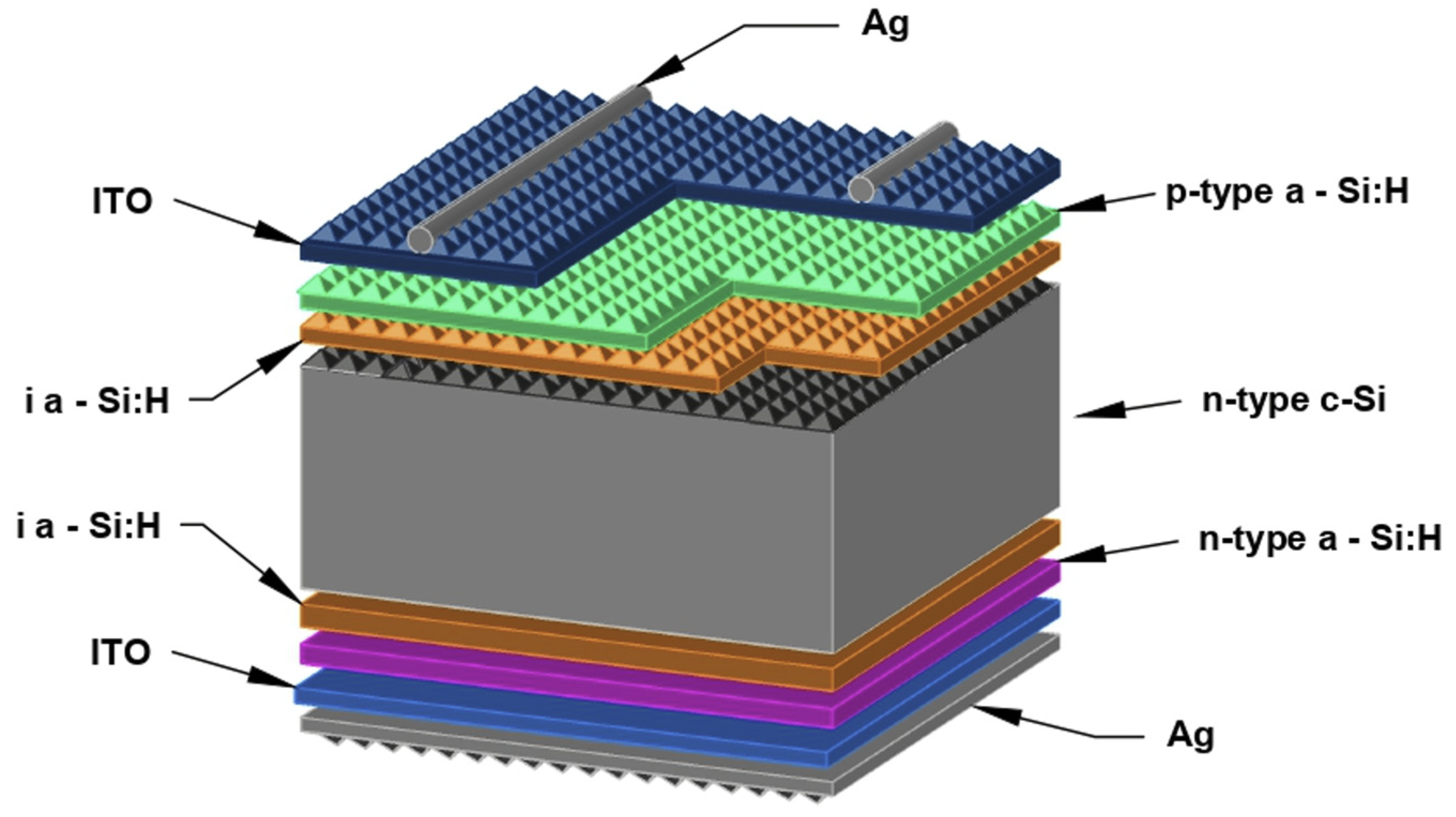
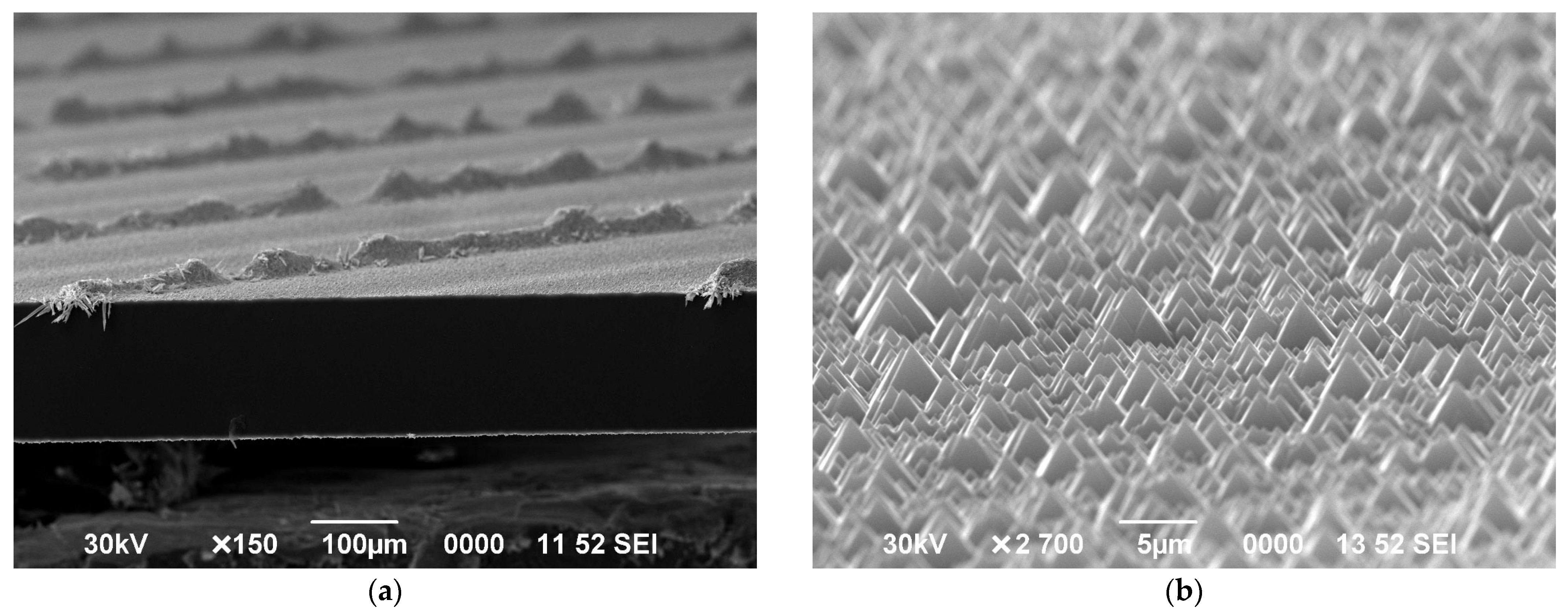
2. Materials and Methods
- (1)
- Degreasing at 65 °C, 1% KOH + 1% H2O2
- (2)
- Etching with 10% KOH
- (3)
- Texturizing with 1% KOH, + 6% IPA
- (4)
- Degreasing at 65 °C, 4 min, 1% KOH + 1% H2O2
- (5)
- Metal removal at 20 °C, 3 min, HF + HCl 1:1
- (6)
- Obtaining an oxide layer at 40% HNO3
- (7)
- Oxide film removal at 20 °C, 8% HF.
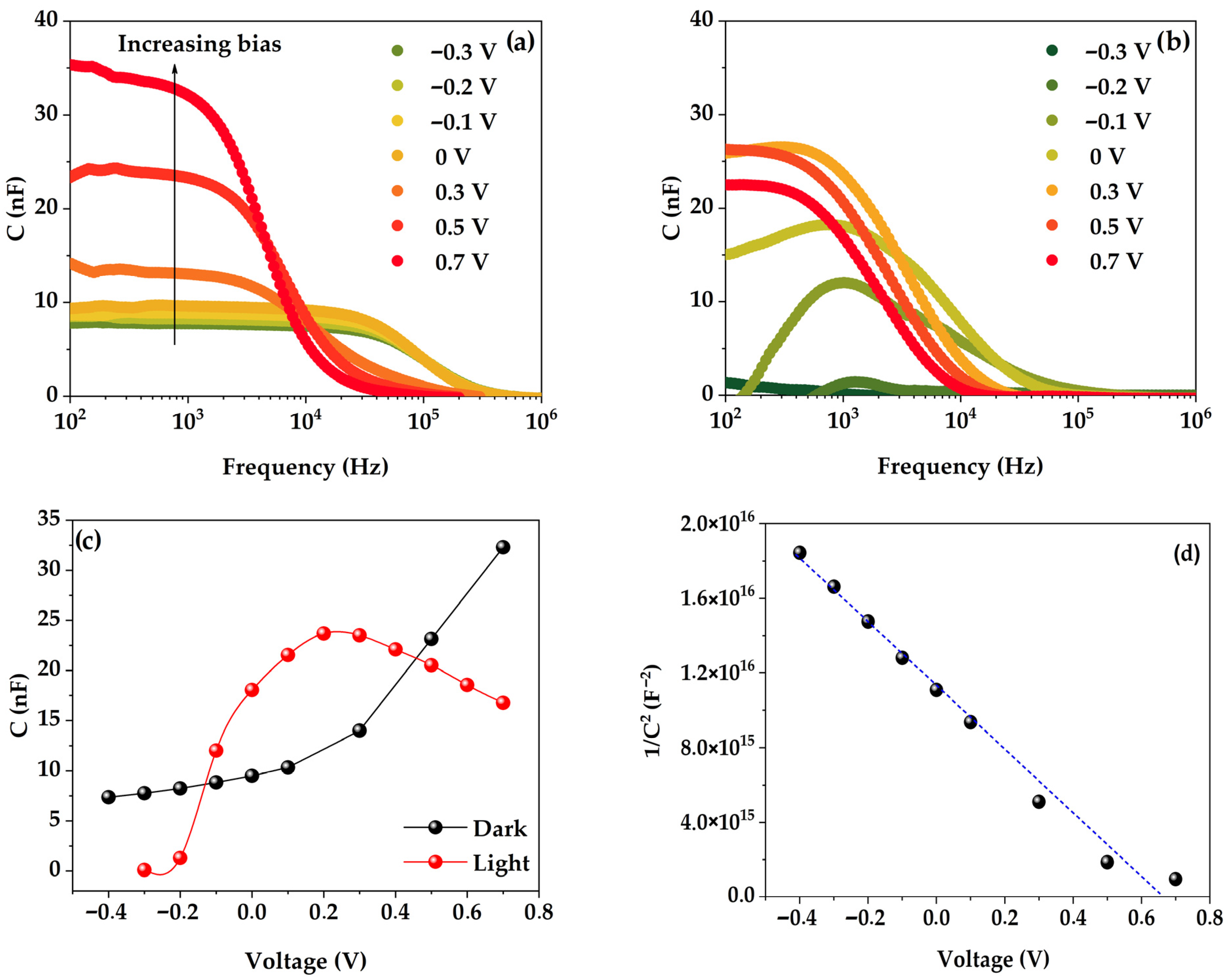
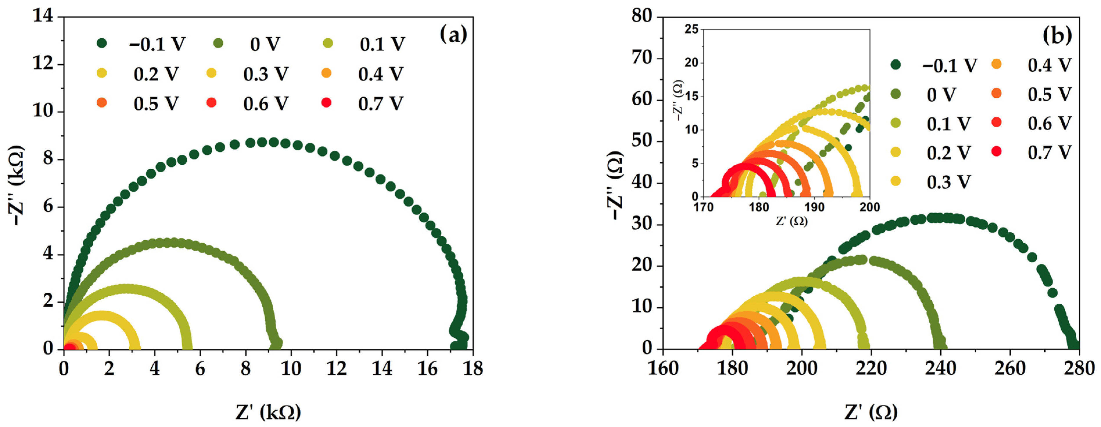
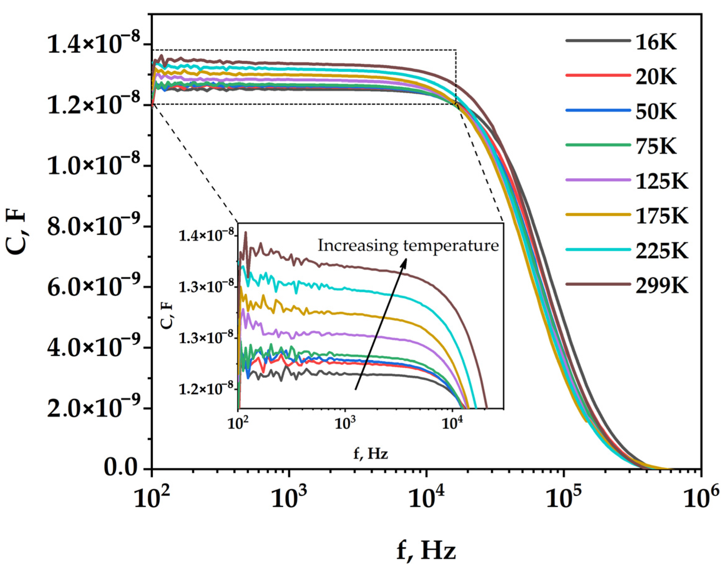
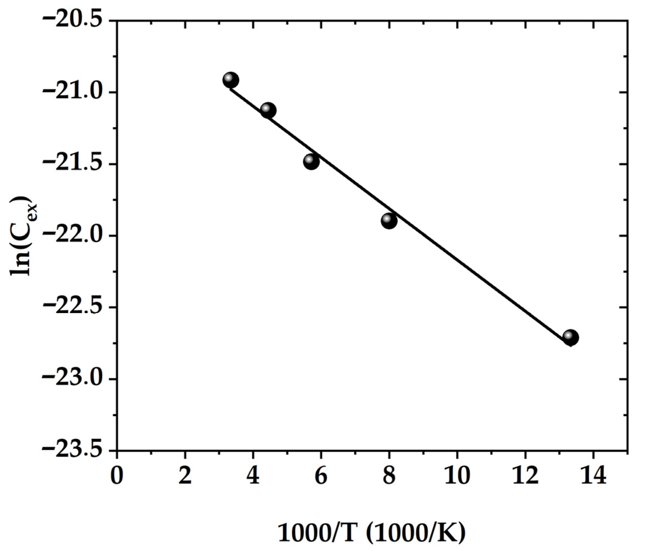
3. Results

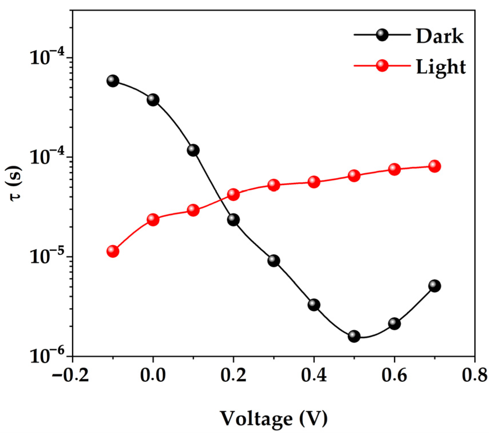
| Structure | ND, cm−3 | Vbi, V | τrelax,dark,Isc, μs | τlight,Voc, μs | η, % | FF | JSC, mA/cm2 | VOC, V | Reference |
|---|---|---|---|---|---|---|---|---|---|
| n+pp+ (p-type Si) (B) | - | 0.96 | - | 1 | 9.0 | 0.65 | 24.2 | 0.577 | [6] |
| npp+ (p-type Si) (A) | - | 0.76 | - | 10 | 9.2 | 0.61 | 27.7 | 0.546 | [6] |
| PEDOT:PSS(rGO) (n-type Si) | 2.48 × 10¹⁸ | 0.34 | 0.017 | - | 0.02 | 0.21 | 40.5 | 0.2 | [38] |
| npp+ (BP ‘‘Saturn’’) (p-type Si) | 3.92 × 10¹⁶ | 0.71 | - | 20 | 12.0 | 0.70 | 35.0 | 0.480 | [19] |
| n+p (A) (p-type Si) | 1.1 × 10¹⁶ | 0.69 | ~200 | - | 17.0 | 0.70 | 38.1 | 0.617 | [2] |
| p+nn+ (n-type Si) | 6.42 × 10¹⁶ | 0.67 | 374 | 83 | 20.1 | 0.759 | 36.7 | 0.721 | This work |
4. Conclusions
Author Contributions
Funding
Data Availability Statement
Conflicts of Interest
References
- Polman, A.; Knight, M.; Garnett, E.C.; Ehrler, B.; Sinke, W.C. Photovoltaic Materials: Present Efficiencies and Future Challenges. Sciences 2016, 352, aad4424. [Google Scholar] [CrossRef]
- Braña, A.F.; Forniés, E.; López, N.; García, B.J. High Efficiency Si Solar Cells Characterization Using Impedance Spectroscopy Analysis. J. Phys. Conf. Ser. 2015, 647, 012069. [Google Scholar] [CrossRef]
- Kumar, R.A.; Suresh, M.S.; Nagaraju, J. Measurement of AC Parameters of Gallium Arsenide (GaAs/Ge) Solar Cell by Impedance Spectroscopy. IEEE Trans. Electron Devices 2001, 48, 2177–2179. [Google Scholar] [CrossRef]
- Panigrahi, J.; Vandana; Singh, R.; Batra, N.; Gope, J.; Sharma, M.; Pathi, P.; Srivastava, S.K.; Rauthan, C.M.S.; Singh, P.K. Impedance Spectroscopy of Crystalline Silicon Solar Cell: Observation of Negative Capacitance. Sol. Energy 2016, 136, 412–420. [Google Scholar] [CrossRef]
- Fabregat-Santiago, F.; Bisquert, J.; Garcia-Belmonte, G.; Boschloo, G.; Hagfeldt, A. Influence of Electrolyte in Transport and Recombination in Dye-Sensitized Solar Cells Studied by Impedance Spectroscopy. Sol. Energy Mater. Sol. Cells 2005, 87, 117–131. [Google Scholar] [CrossRef]
- Garcia-Belmonte, G.; García-Cañadas, J.; Mora-Seró, I.; Bisquert, J.; Voz, C.; Puigdollers, J.; Alcubilla, R. Effect of Buffer Layer on Minority Carrier Lifetime and Series Resistance of Bifacial Heterojunction Silicon Solar Cells Analyzed by Impedance Spectroscopy. Thin Solid Film. 2006, 514, 254–257. [Google Scholar] [CrossRef]
- Daliento, S.; Tari, O.; Lancellotti, L. Closed-Form Analytical Expression for the Conductive and Dissipative Parameters of the MOS-C Equivalent Circuit. IEEE Trans. Electron Devices 2011, 58, 3643–3646. [Google Scholar] [CrossRef]
- Von Hauff, E. Impedance Spectroscopy for Emerging Photovoltaics. J. Phys. Chem. C 2019, 123, 11329–11346. [Google Scholar] [CrossRef]
- Jensen, N.; Hausner, R.M.; Bergmann, R.B.; Werner, J.H.; Rau, U. Optimization and Characterization of Amorphous/Crystalline Silicon Heterojunction Solar Cells. Prog. Photovolt. Res. Appl. 2002, 10, 1–13. [Google Scholar] [CrossRef]
- Fujiwara, H.; Kondo, M. Effects of A-Si:H Layer Thicknesses on the Performance of a-Si:H∕c-Si Heterojunction Solar Cells. J. Appl. Phys. 2007, 101, 054516. [Google Scholar] [CrossRef]
- De Wolf, S.; Descoeudres, A.; Holman, Z.C.; Ballif, C. High-Efficiency Silicon Heterojunction Solar Cells: A Review. Green 2012, 2, 7–24. [Google Scholar] [CrossRef]
- Chapin, D.M.; Fuller, C.S.; Pearson, G.L. A New Silicon P-n Junction Photocell for Converting Solar Radiation into Electrical Power. J. Appl. Phys. 1954, 25, 676–677. [Google Scholar] [CrossRef]
- Fuhs, W.; Niemann, K.; Stuke, J. Heterojunctions of Amorphous Silicon and Silicon Single Crystals. AIP Conf. Proc. 1974, 20, 345–350. [Google Scholar]
- Pankove, J.I.; Tarng, M.L. Amorphous Silicon as a Passivant for Crystalline Silicon. Appl. Phys. Lett. 1979, 34, 156–157. [Google Scholar] [CrossRef]
- Hamakawa, Y.; Fujimoto, K.; Okuda, K.; Kashima, Y.; Nonomura, S.; Okamoto, H. New Types of High Efficiency Solar Cells Based on a -Si. Appl. Phys. Lett. 1983, 43, 644–646. [Google Scholar] [CrossRef]
- Okuda, K.; Okamoto, H.; Hamakawa, Y. Amorphous Si/Polycrystalline Si Stacked Solar Cell Having More Than 12% Conversion Efficiency. Jpn. J. Appl. Phys. 1983, 22, L605. [Google Scholar] [CrossRef]
- Matsuura, H.; Okuno, T.; Okushi, H.; Tanaka, K. Electrical Properties of n -Amorphous/ p -Crystalline Silicon Heterojunctions. J. Appl. Phys. 1984, 55, 1012–1019. [Google Scholar] [CrossRef]
- Tanaka, M.; Taguchi, M.; Matsuyama, T.; Sawada, T.; Tsuda, S.; Nakano, S.; Hanafusa, H.; Kuwano, Y. Development of New A-Si/c-Si Heterojunction Solar Cells: ACJ-HIT (Artificially Constructed Junction-Heterojunction with Intrinsic Thin-Layer). Jpn. J. Appl. Phys. 1992, 31, 3518. [Google Scholar] [CrossRef]
- Mora-Seró, I.; Garcia-Belmonte, G.; Boix, P.P.; Vázquez, M.A.; Bisquert, J. Impedance Spectroscopy Characterisation of Highly Efficient Silicon Solar Cells under Different Light Illumination Intensities. Energy Environ. Sci. 2009, 2, 678. [Google Scholar] [CrossRef]
- Lee, S.; Park, S.; Park, J.; Kim, Y.; Park, H.; Jang, J.; Shin, C.; Lee, Y.-J.; Baek, S.; Kim, M.; et al. Impedance Spectroscopic Study of P-i-n Type a-Si Solar Cell by Doping Variation of p-Type Layer. Int. J. Photoenergy 2012, 2012, 767248. [Google Scholar] [CrossRef]
- Bouzidi, A.; Jilani, W.; Yahia, I.S.; Zahran, H.Y. Impedance Spectroscopy of Monocrystalline Silicon Solar Cells for Photosensor Applications: Highly Sensitive Device. Phys. B Condens. Matter 2020, 596, 412375. [Google Scholar] [CrossRef]
- Orpella, A.; Martín, I.; López-González, J.M.; Ortega, P.; Muñoz, J.; Sinde, D.C.; Voz, C.; Puigdollers, J.; Alcubilla, R. Experimental Determination of Base Resistance Contribution for Point-like Contacted c-Si Solar Cells Using Impedance Spectroscopy Analysis. Sol. Energy Mater. Sol. Cells 2015, 141, 350–355. [Google Scholar] [CrossRef]
- Matacena, I.; Lancellotti, L.; Lisi, N.; Delli Veneri, P.; Guerriero, P.; Daliento, S. Impedance Spectroscopy for the Characterization of the All-Carbon Graphene-Based Solar Cell. Energies 2020, 13, 1908. [Google Scholar] [CrossRef]
- van Nijen, D.A.; Muttillo, M.; Van Dyck, R.; Poortmans, J.; Zeman, M.; Isabella, O.; Manganiello, P. Revealing Capacitive and Inductive Effects in Modern Industrial C-Si Photovoltaic Cells through Impedance Spectroscopy. Sol. Energy Mater. Sol. Cells 2023, 260, 112486. [Google Scholar] [CrossRef]
- Shehata, M.M.; Truong, T.N.; Basnet, R.; Nguyen, H.T.; Macdonald, D.H.; Black, L.E. Impedance Spectroscopy Characterization of C-Si Solar Cells with SiOx/ Poly-Si Rear Passivating Contacts. Sol. Energy Mater. Sol. Cells 2023, 251, 112167. [Google Scholar] [CrossRef]
- Panigrahi, J.; Pandey, A.; Bhattacharya, S.; Pal, A.; Mandal, S.; Krishna Komarala, V. Impedance Spectroscopy of Amorphous/Crystalline Silicon Heterojunction Solar Cells under Dark and Illumination. Sol. Energy 2023, 259, 165–173. [Google Scholar] [CrossRef]
- Garland, J.E.; Crain, D.J.; Roy, D. Impedance Spectroscopy Coupled with Voltammetry for Quantitative Evaluation of Temperature and Voltage Dependent Parameters of a Silicon Solar Cell. Sol. Energy 2011, 85, 2912–2923. [Google Scholar] [CrossRef]
- Yadav, P.; Pandey, K.; Bhatt, V.; Kumar, M.; Kim, J. Critical Aspects of Impedance Spectroscopy in Silicon Solar Cell Characterization: A Review. Renew. Sustain. Energy Rev. 2017, 76, 1562–1578. [Google Scholar] [CrossRef]
- Ballif, C.; Haug, F.-J.; Boccard, M.; Verlinden, P.J.; Hahn, G. Status and Perspectives of Crystalline Silicon Photovoltaics in Research and Industry. Nat. Rev. Mater. 2022, 7, 597–616. [Google Scholar] [CrossRef]
- Chuchvaga, N.A.; Schulze, J.; Klimenov, V.V.; Zholdybayev, K.S.; Aimaganbetov, K.P.; Zhantuarov, S.R.; Serikkanov, A.S.; Terukov, E.I.; Tokmoldin, S.Z.; Tokmoldin, N.S. Optimization and Fabrication of Heterojunction Silicon Solar Cells Using an Experimental-Industrial Facility AK-1000 Inline. J. Russ. Univ. Radioelectron. 2020, 23, 57–62. [Google Scholar] [CrossRef]
- Chuchvaga, N.A.; Kislyakova, N.M.; Tokmoldin, N.S.; Rakymetov, B.A.; Serikkanov, A.S. Problems Arising from Using KOH–IPA Etchant to Texture Silicon Wafers. Tech. Phys. 2020, 65, 1685–1689. [Google Scholar] [CrossRef]
- Aimaganbetov, K.P.; Aldiyarov, A.U.; Zhantuarov, S.R.; Almasov, N.Z.; Terukov, E.I.; Tokmoldin, N.S. A Low Temperature Cell for High Frequency Electrophysical Measurements of Semiconductor Devices. Instrum. Exp. Tech. 2021, 64, 886–890. [Google Scholar] [CrossRef]
- Aimaganbetov, K.; Almas, N.; Kurbanova, B.; Muratov, D.; Serikkanov, A.; Insepov, Z.; Tokmoldin, N. Electrical and Structural Characterization of Few-Layer Graphene Sheets on Quartz. Materials 2022, 15, 5330. [Google Scholar] [CrossRef] [PubMed]
- Han, Y.; Yu, X.; Wang, D.; Yang, D. Formation of Various Pyramidal Structures on Monocrystalline Silicon Surface and Their Influence on the Solar Cells. J. Nanomater. 2013, 2013, 716012. [Google Scholar] [CrossRef]
- Matacena, I.; Guerriero, P.; Lancellotti, L.; Bobeico, E.; Lisi, N.; Chierchia, R.; Delli Veneri, P.; Daliento, S. Forward Bias Capacitance Investigation as a Powerful Tool to Monitor Graphene/Silicon Interfaces. Sol. Energy 2021, 226, 1–8. [Google Scholar] [CrossRef]
- Gelderman, K.; Lee, L.; Donne, S.W. Flat-Band Potential of a Semiconductor: Using the Mott–Schottky Equation. J. Chem. Educ. 2007, 84, 685. [Google Scholar] [CrossRef]
- Mahapatra, A.; Parikh, N.; Kumar, P.; Kumar, M.; Prochowicz, D.; Kalam, A.; Tavakoli, M.M.; Yadav, P. Changes in the Electrical Characteristics of Perovskite Solar Cells with Aging Time. Molecules 2020, 25, 2299. [Google Scholar] [CrossRef] [PubMed]
- Behura, S.; Haokip, H.; Goel, C.; Nayak, S.; Mahala, P.; Kapadia, R.; Jani, O. Photovoltaic and Impedance Spectroscopic Characteristics of Heterojunction of Graphene-PEDOT:PSS Composite and n-Silicon Prepared via Solution-Based Process. Mater. Res. Innov. 2017, 21, 263–268. [Google Scholar] [CrossRef]
- Schroder, D.K. Semiconductor Material and Device Characterization, 3rd ed.; John Wiley & Sons, Inc.: New York, NY, USA, 2005; ISBN 0471739065. [Google Scholar]
- Bisquert, J.; Fabregat-Santiago, F.; Mora-Seró, I.; Garcia-Belmonte, G.; Giménez, S. Electron Lifetime in Dye-Sensitized Solar Cells: Theory and Interpretation of Measurements. J. Phys. Chem. C 2009, 113, 17278–17290. [Google Scholar] [CrossRef]
- Fakharuddin, A.; Ahmed, I.; Wali, Q.; Khalidin, Z.; Yusoff, M.M.; Rajan, J. Probing Electron Lifetime and Recombination Dynamics in Large Area Dye-Sensitized Solar Cells by Electrochemical Impedance Spectroscopy. Adv. Mater. Res. 2014, 925, 553–558. [Google Scholar] [CrossRef]
- Leon, C.; Le Gall, S.; Gueunier-Farret, M.-E.; Kleider, J.-P. How to Perform Admittance Spectroscopy and DLTS in Multijunction Solar Cells. Sol. Energy Mater. Sol. Cells 2022, 240, 111699. [Google Scholar] [CrossRef]
- Cai, J.; Chen, X.; Hong, R.; Yang, W.; Wu, Z. High-Performance 4H-SiC-Based p-i-n Ultraviolet Photodiode and Investigation of Its Capacitance Characteristics. Opt. Commun. 2014, 333, 182–186. [Google Scholar] [CrossRef]
- Kalam, A.; Runjhun, R.; Mahapatra, A.; Tavakoli, M.M.; Trivedi, S.; Tavakoli Dastjerdi, H.; Kumar, P.; Lewiński, J.; Pandey, M.; Prochowicz, D.; et al. Interpretation of Resistance, Capacitance, Defect Density, and Activation Energy Levels in Single-Crystalline MAPbI 3. J. Phys. Chem. C 2020, 124, 3496–3502. [Google Scholar] [CrossRef]
- Yang, K.-J.; Sim, J.-H.; Son, D.-H.; Jeon, D.-H.; Hwang, D.-K.; Nam, D.; Cheong, H.; Kim, S.; Kim, J.; Kim, D.-H.; et al. Comparison of Chalcopyrite and Kesterite Thin-Film Solar Cells. J. Ind. Eng. Chem. 2017, 45, 78–84. [Google Scholar] [CrossRef]
- Hase, H.; Okachi, T.; Ishihara, S.; Nagase, T.; Kobayashi, T.; Naito, H. Impedance Spectroscopy for High Resolution Measurements of Energetic Distributions of Localized States in Organic Semiconductors. Thin Solid Film. 2014, 554, 218–221. [Google Scholar] [CrossRef]
- Carr, J.A.; Elshobaki, M.; Chaudhary, S. Deep Defects and the Attempt to Escape Frequency in Organic Photovoltaic Materials. Appl. Phys. Lett. 2015, 107, 203302. [Google Scholar] [CrossRef]
- Nandal, V.; Agarwal, S.; Nair, P.R. Deciphering the Capacitance Frequency Technique for Performance-Limiting Defect-State Parameters in Energy-Harvesting Perovskites. Phys. Chem. Chem. Phys. 2021, 23, 24421–24427. [Google Scholar] [CrossRef]
- Yang, K.-J.; Kim, S.; Kim, S.-Y.; Ahn, K.; Son, D.-H.; Kim, S.-H.; Lee, S.-J.; Kim, Y.-I.; Park, S.-N.; Sung, S.-J.; et al. Flexible Cu2ZnSn(S,Se)4 Solar Cells with over 10% Efficiency and Methods of Enlarging the Cell Area. Nat. Commun. 2019, 10, 2959. [Google Scholar] [CrossRef]


Disclaimer/Publisher’s Note: The statements, opinions and data contained in all publications are solely those of the individual author(s) and contributor(s) and not of MDPI and/or the editor(s). MDPI and/or the editor(s) disclaim responsibility for any injury to people or property resulting from any ideas, methods, instructions or products referred to in the content. |
© 2024 by the authors. Licensee MDPI, Basel, Switzerland. This article is an open access article distributed under the terms and conditions of the Creative Commons Attribution (CC BY) license (https://creativecommons.org/licenses/by/4.0/).
Share and Cite
Aimaganbetov, K.; Yerezhep, D.; Kishkenebayev, M.; Chuchvaga, N.; Almas, N.; Tokmoldin, S.; Tokmoldin, N. Characterization of a Heterojunction Silicon Solar Cell by Means of Impedance Spectroscopy. Micromachines 2024, 15, 184. https://doi.org/10.3390/mi15020184
Aimaganbetov K, Yerezhep D, Kishkenebayev M, Chuchvaga N, Almas N, Tokmoldin S, Tokmoldin N. Characterization of a Heterojunction Silicon Solar Cell by Means of Impedance Spectroscopy. Micromachines. 2024; 15(2):184. https://doi.org/10.3390/mi15020184
Chicago/Turabian StyleAimaganbetov, Kazybek, Darkhan Yerezhep, Mussabek Kishkenebayev, Nikolay Chuchvaga, Nurlan Almas, Serekbol Tokmoldin, and Nurlan Tokmoldin. 2024. "Characterization of a Heterojunction Silicon Solar Cell by Means of Impedance Spectroscopy" Micromachines 15, no. 2: 184. https://doi.org/10.3390/mi15020184