Article

A Comprehensive Analysis of Unclamped-Inductive-Switching-Induced Electrical Parameter Degradations and Optimizations for 4H-SiC Trench Metal-Oxide-Semiconductor Field-Effect Transistor Structures

by
Li Liu
1,*,
Jingqi Guo
2,
Yiheng Shi
2,
Kai Zeng
2 and
Gangpeng Li
1
1
State Key Laboratory of Wide-Bandgap Semiconductor Devices and Integrated Technology, School of Microelectronics, Xidian University, Xi’an 710071, China
2
Guangzhou Institute of Technology, Xidian University, Guangzhou 510555, China
*
Author to whom correspondence should be addressed.
Micromachines 2024, 15(6), 772; https://doi.org/10.3390/mi15060772
Submission received: 13 May 2024 / Revised: 1 June 2024 / Accepted: 7 June 2024 / Published: 9 June 2024

Abstract

:
This paper presents a comprehensive study on single- and repetitive-frequency UIS characteristics of 1200 V asymmetric (AT) and double trench silicon carbide (DT-SiC) metal-oxide-semiconductor field-effect transistors (MOSFETs) and their electrical degradation under electrical–thermal working conditions, investigated through experiment and simulation verification. Because their structure is different, the failure mechanisms are different. Comparatively, the gate oxide of a DT-MOSFET is more easily damaged than an AT-MOSFET because the hot carriers are injected into the oxide. The parameters’ degradation under repetitive UIS stress also requires analysis. The variations in the measured parameters are recorded to evaluate typical electrical features of device failure. Furthermore, TCAD simulation is used to reveal the electrothermal stress inside the device during avalanche. Additionally, failed devices are decapsulated to verify the location of the failure point. Finally, a new type of stepped-oxide vertical power DT MOSFET with P-type shielding and current spread layers, along with its feasible process flow, is proposed for the improvement of gate dielectric reliability.

1. Introduction

Due to its wide bandgap, highly critical breakdown electrical field, and thermal conductivity, SiC is recognized as the most promising candidate for high-temperature and high-power applications [1,2,3].
Because intrinsic SiO2 is used as the gate dielectric, SiC vertical power MOSFETs possess simultaneous advantages of high switching speed and high power, enabling the devices to be widely applied in power market areas such as photovoltaic inverters, electric vehicles, electric aircraft, uninterruptible power supplies, and energy distribution networks. Under these application scenarios, high dv/dt and di/dt [4] could be generated during high-speed switching. If the inductive load is used, an induced voltage will be generated and stressed between the drain and source of the DUT during the fast turn-on and turn-off transient because the variation in the current that flows through the load inductor cannot track the one in loop synchronously. If the induced voltage exceeds the breakdown voltage of the devices, the devices will be forced into avalanche mode. The energy stored in the load inductor will be released through the power devices at the turn-off point. Simultaneous high voltage and large current can stress the devices, potentially leading to the failure of the devices [5,6,7].
Until now, many researchers have focused on UIS phenomena of planar MOSFETs. It is generally believed that there are two possible reasons for a single UIS failure of the device [8,9,10,11,12,13,14,15,16,17,18,19]: One is the turn-on of parasitic BJT triggering positive thermal-electrical feedback, ultimately leading to device failure. The other is high junction temperature causing the aluminum metal to melt, resulting in device failure. As to a repetitive UIS failure mechanism, it is commonly believed that a hot hole in the JFET region will be injected into oxide and trapped by the interface states and gate oxide leading to the parameters’ degradation. However, there are fewer comprehensive studies [7,20,21] on UIS failure mechanisms including temperature characteristics and some important circuit loop parameters under single and repetitive UIS stress on trench gate MOSFETs.
In this paper, a comprehensive study of single- and repetitive-frequency UIS characteristics of 1200 V AT-MOSFETs and DT-SiC MOSFETs under different working conditions are investigated by experiment and simulation, i.e., Rohm DT-MOSFETs and Infineon AT-MOSFETs with the same current rate and on-state resistance. The single-pulse UIS and repetitive UIS measurements were performed on these two kinds of devices. Degradation and failure mechanisms of devices have been researched through the combination of measured data, numerical simulation, and microstructure analysis. A reasonable physical failure explanation during avalanche has been given. Additionally, failed devices have been decapsulated to verify the location of the failure point from the perspective of the semiconductor die. Finally, a new type of vertical power DT MOSFET is proposed for the improvement of the gate’s dielectric reliability.

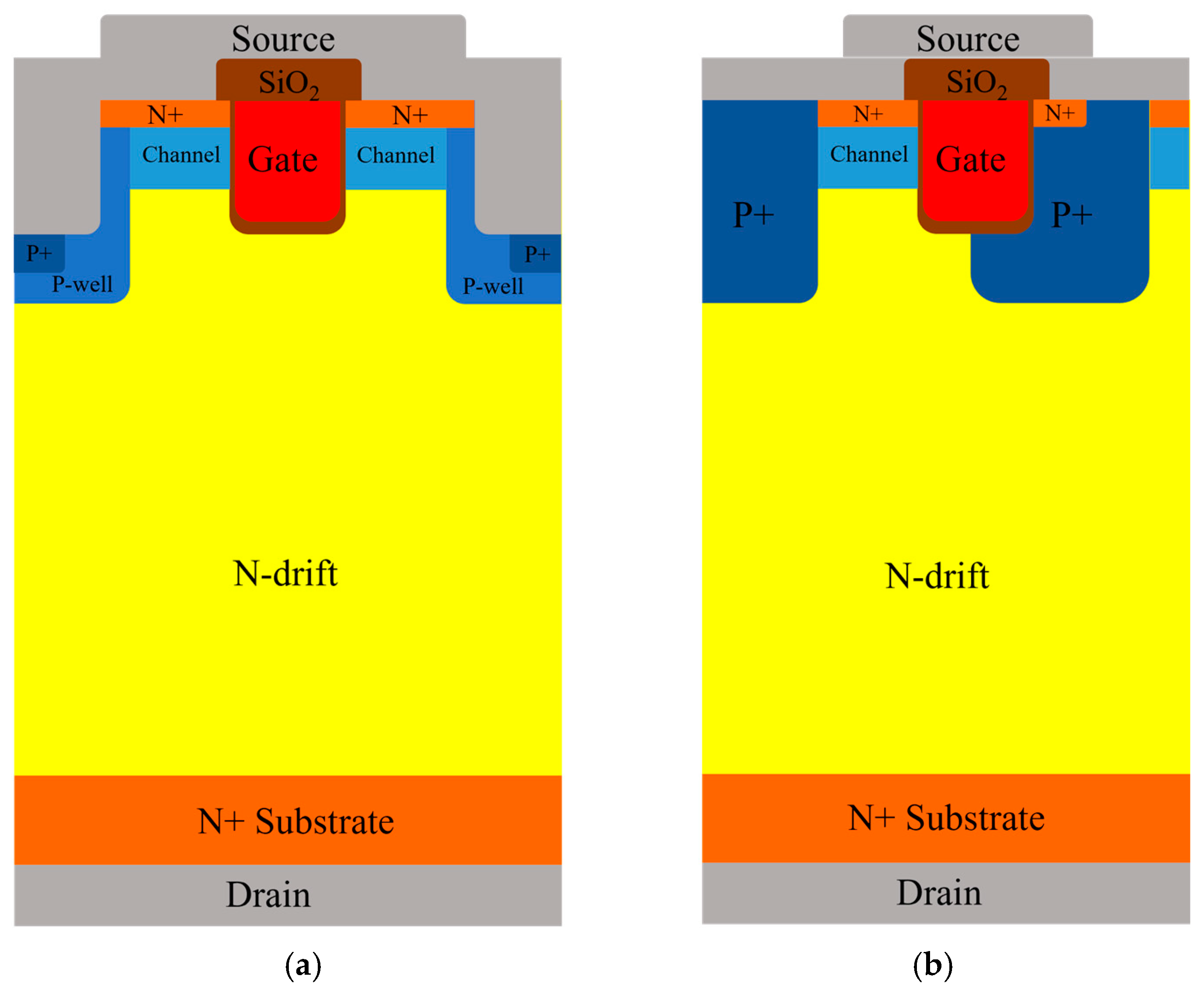
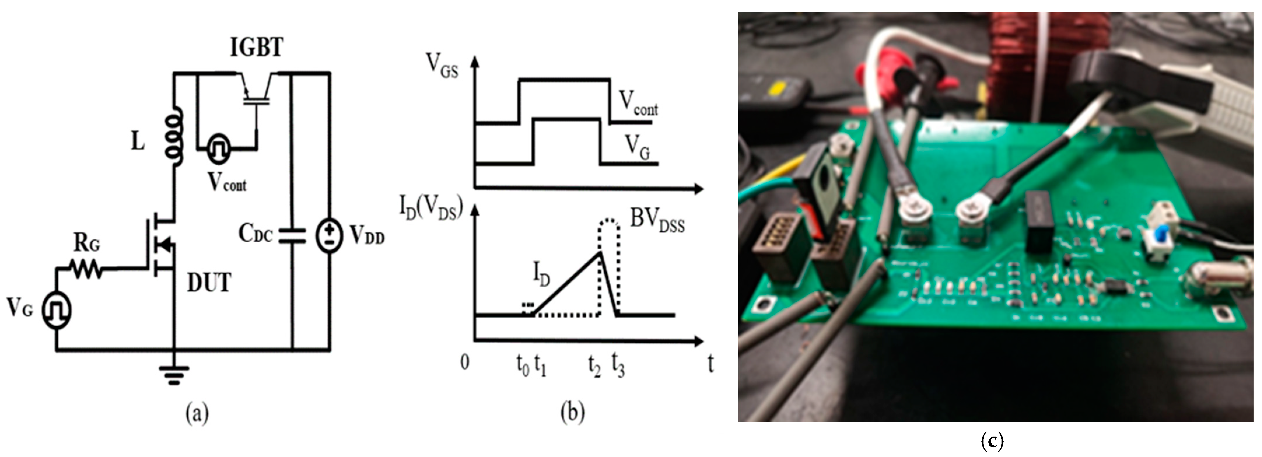
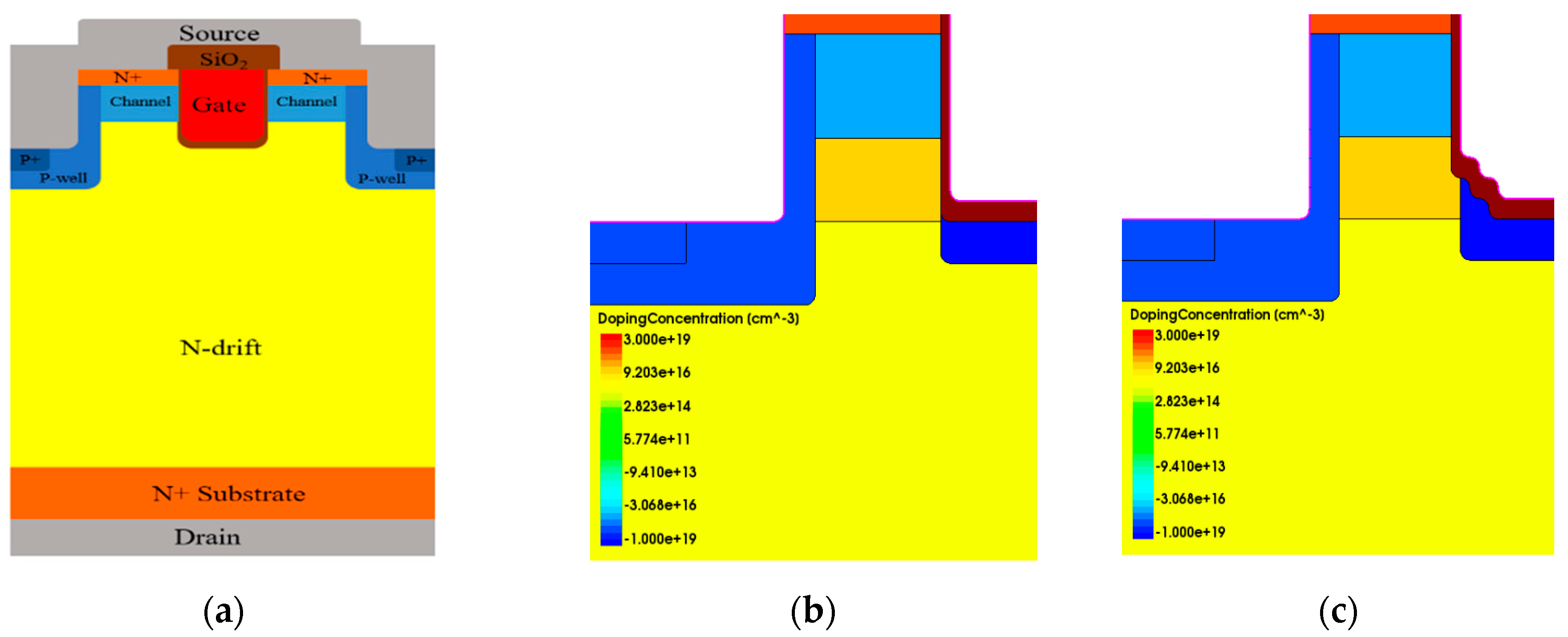
2. Device Structures and Experimental Setup

The measurements were taken using devices under test (DUTs) listed as Rohm SCT3080 as shown in Figure 1a as a symmetrical double-trench SiC MOSFET rated at 4.2 V, 30 A, 1200 V, and 80 mΩ with an area of 2.4 mm × 3.0 mm. IMZ120R090M1HXKSA1 is shown in Figure 1b as an asymmetrical trench SiC MOSFET rated at 4.5 V, 26 A, 1200 V, and 90 mΩ with an area of 2.2 mm × 2.1 mm. All were encapsulated in TO-247-3 packages.
Figure 2 shows the circuit diagram (a) and wave curve diagrams (b). Figure 2c shows the image of UIS test setup. The main circuit includes two parts: driver circuit and power loop. The driver circuit is composed of driver source, gate resistance RG, and the DUT. The power loop includes a DC voltage source VDD, a DC-stabilizing capacitor CDC, a load inductor L, and the DUT. Both DUT and Si IGBT act as charging switch to control load inductor L. Si IGBT will isolate DUT from DC bus. In this circuit, when IGBT module and VG turn off simultaneously, it ensures that DC bus does not participate in energy dissipating during avalanche events. During the whole measurement, VDD could be set much higher than the avalanche voltage of DUT; thus, the conduction time can be decreased and thereby helps to reduce heat generation.
Figure 2b depicts the waveform diagrams where BVDSS is avalanche voltage, t3–t2 is avalanche time tav, and t2–t1 is charging time of load inductor. The DC power supply voltage was set to 50 V. The gate voltage was switched from −3 to +15 V, several 20 Ω resistors were parallelly connected between the gate driver and MOSFET, and the load inductor was chosen to be 3 mH. As can be seen from Figure 2a and the waveforms in Figure 2b, when the IGBT and DUT turn on at the same moment, the current flowing through the inductor increases linearly. When the pre-set maximum current value is achieved, the energy stored in inductor forces DUT to enter avalanche mode simultaneously when the DUT turns off.

3. Parameter Degradation and Avalanche Ruggedness Analysis

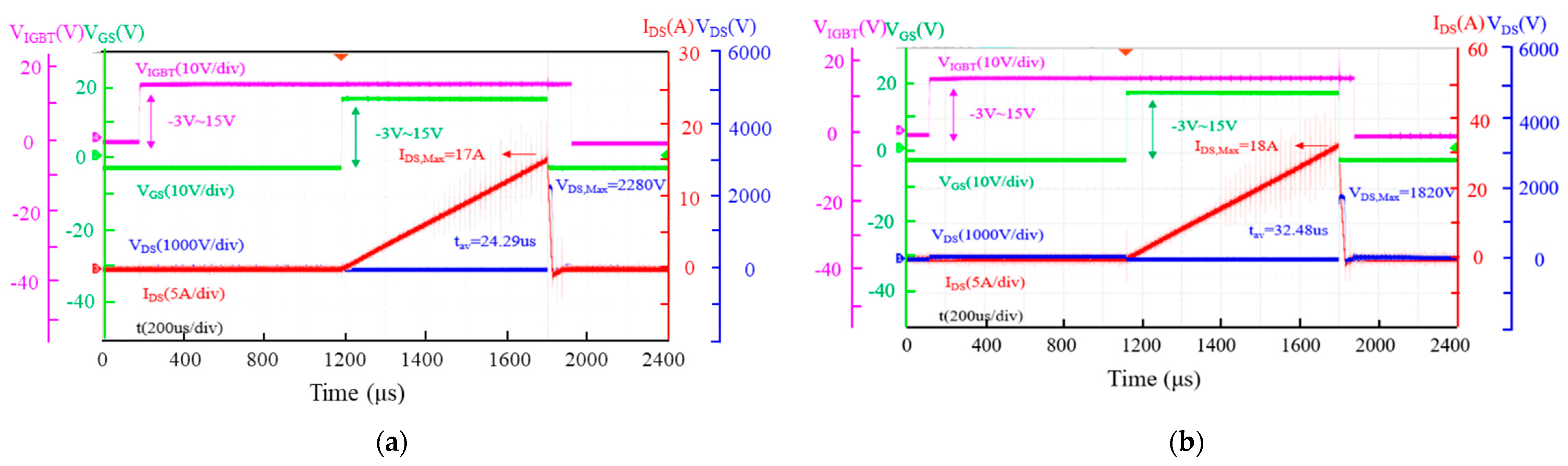
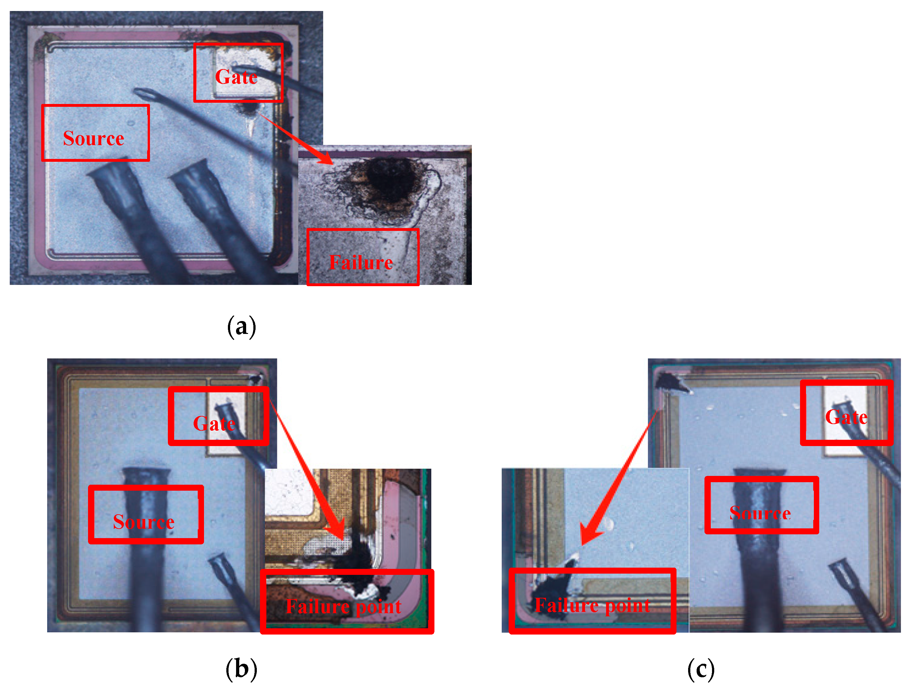
3.1. Single UIS Test

Figure 3 and Figure 4 show the typical single UIS waveforms of AT-MOSFETs and DT-MOSFETs during the last test before failure (Figure 3) and at failure (Figure 4) under 3.0 mH of inductive load conditions, respectively. When the MOSFET turns on, the IDS rises linearly to the maximum drain-source current (IDS, Max) with a slope of VDD/L. After it turns off, the energy stored in the inductive load forces the MOSFET to enter into avalanche mode. At this moment, the VDS maintains breakdown voltage and the IDS gradually decreases to zero from IDS, max. For AT-MOSFETs, the peak drain current and the voltage across the drain to the source are 18 A and 1820 V during avalanche, respectively. The avalanche state lasts for 32.48 us, while the gate pulse width reaches 1.08 ms. Avalanche energy is 0.53 J. When avalanche occurs, as shown in Figure 4b, the gate pulse width increase to 1.14 ms, the peak drain current increase to 19 A, and avalanche voltage remains 1820 V. The avalanche time lasts for 18.45 us, then the DUT fails, which means that the blocking capability is lost between the source and the drain. Comparatively, for DT-MOSFETs, before failure, the avalanche current and voltage are respectively 17 A and 2280 V, the avalanche state lasts for about 24.29 us, and the gate pulse width reaches 1.02 ms. Avalanche energy is 0.47 J. When avalanche occurs, the current reaches 18 A and the gate pulse width reaches 1.08 ms, while the avalanche state lasts for only 30.45 ns because of the longer gate pulse width than the one before failure. At this moment, more avalanche energy is injected into the parasitic pn-diode, and the pn-diode cannot withstand it. Then, after the avalanche state has lasted for only 30.45 ns, the device fails. In Figure 4a,b, because of the IGBT module protection (as marked with a black arrow), thermal away did not occur in our test and the current increase was shut down by the turn-off of the IGBT module.
Table 1 presents the IDS,Max, VDS,max, EAV, and tAV of the DUTs under the single UIS test with different inductive loads. We can see from this table that the avalanche withstanding capability gradually increases with the increase in inductor load. The peak avalanche current presents a decreasing trend, while the avalanche duration gradually increases.
The EAV of AT-MOSFETs is higher than that of DT-MOSFETs, which means superior single UIS ruggedness than SiC MOSFETs with an AT structure. Also, higher EAV indicates serious thermal stress in SiC MOSFETs, so the avalanche voltage of 2240 V makes DT-MOSFETs more susceptible than AT-MOSFETs to gate oxide reliability.
Figure 5 gives the dependence of tAV and EAV on on-state time ton for both AT-MOSFETs (a) and DT-MOSFETs (b) with a fixed load inductor value. In these two figures, a symbol plus a dashed line represents tAV versus ton and a symbol plus a solid line represents Eav versus ton. Different temperature characteristics can be distinguished by a black, solid square (25 °C); a red, solid circle (75 °C); a blue, solid, right-way-up triangle (125 °C); and a green, solid, upside-down triangle (175 °C). All measurement dates are recorded before the DUT failure occurs. In our measurements, since DT- and AT-MOSFETs have the same electrical characteristics ratio regarding breakdown voltage and current, the maximum current IDS,Max flowing inductor when avalanche occurs also has the same value. We can see from Figure 2b that tAV ∝ 1/BV, and BV increases with increasing temperature, and thus tAV will decrease a little with the increasing temperature, linearly proportional to ton. EAV is exponential to ton, which is pre-set by the tester and is independent of temperature, so EAV overlaps for both devices in the temperature range.
Figure 6 presents the dependence of tav and Eav for DT- and AT-SiC MOSFETs on ambient temperature with a load inductor equal to 3 mH in UIS conditions. For these two types of transistors, a different variation with temperature is observed. For AT-MOSFETs, tav and Eav decrease a little bit as the temperature increases. From 25 °C to 175 °C, the maximum tav decreased by approximately 3% and the maximum Eav decreased by about 6%. While, for DT-MOSFETs, comparatively, as the ambient temperature increases, both tav and Eav increase monotonically. From 25 °C to 175 °C, tav increased by approximately 7% and the maximum Eav increased significantly, by 26%. So, the temperature has a significant impact on the avalanche energy of DT MOSFETs.
Figure 7 shows the peak avalanche current (Ipeak), start point of avalanche voltage (BVst), and peak avalanche voltage (Vpeak) at failure of DT MOSFETs and AT MOSFETs with a fixed 3 mH load inductor. This figure shows that, for AT MOSFETs, the peak point of avalanche voltage and start point of avalanche voltage has increased as the ambient temperature increased, while the peak avalanche current at failure has decreased first and then stayed almost constant. For DT MOSFETs, these three electrical parameters all show a monotonously increasing trend with temperature. The start point and peak point avalanche voltage also increase monotonously.
Figure 8 shows the decapsulation images and failure point of AT-MOSFETs and DT-MOSFETs under a single UIS test. For AT-MOSFETs, the failure point is obviously located at the point beside the gate electrode and on the source electrode.
Figure 8b,c present the decapsulation images and failure points of a DT-MOSFET at 25 °C and 175 °C. During our measurements, when the gate driver signal is switched off, the gate voltage does not immediately drop to zero, which is marked in Figure 4a, and this phenomenon indicates that the avalanche current is flowing not only from drain to source, but also through the gate to the source, leading to abnormal gate voltage. Thus, the DT-MOSFET is susceptible to gate oxide damage. As demonstrated in Figure 8a,b, an obvious crack is found above the gate electrode. It can be thought that the failure is because of gate oxide damage [10,22,23].

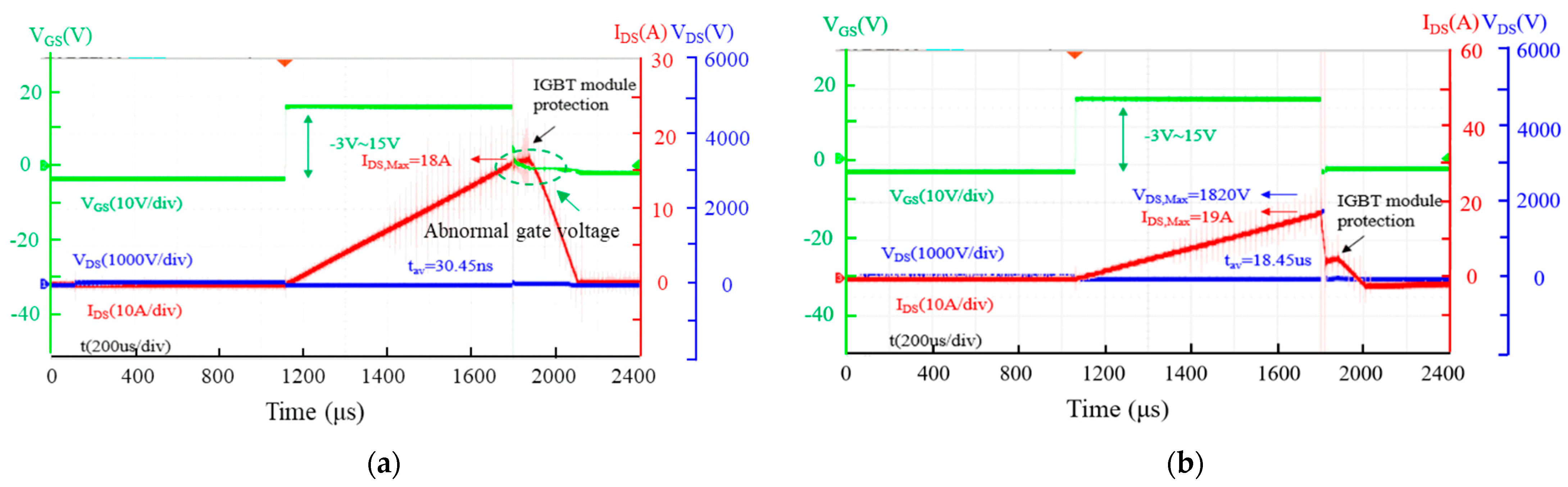
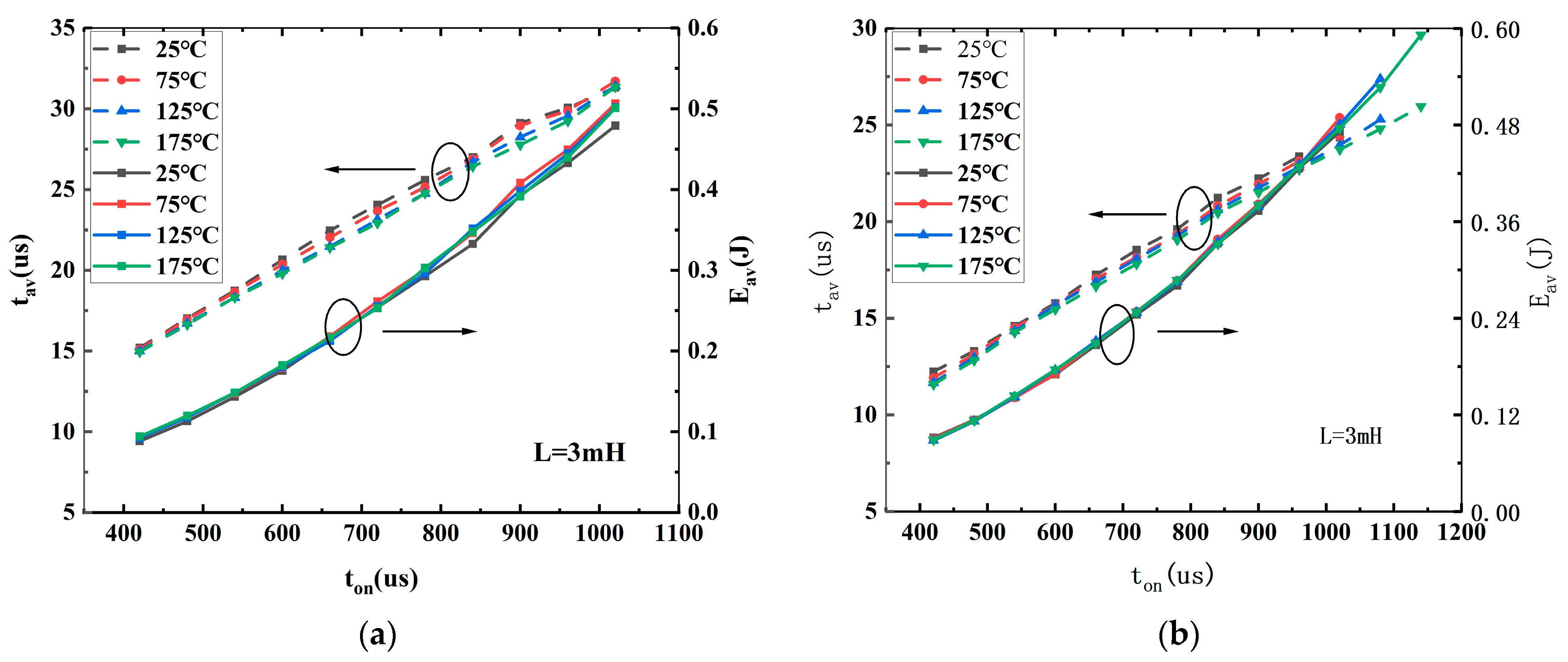
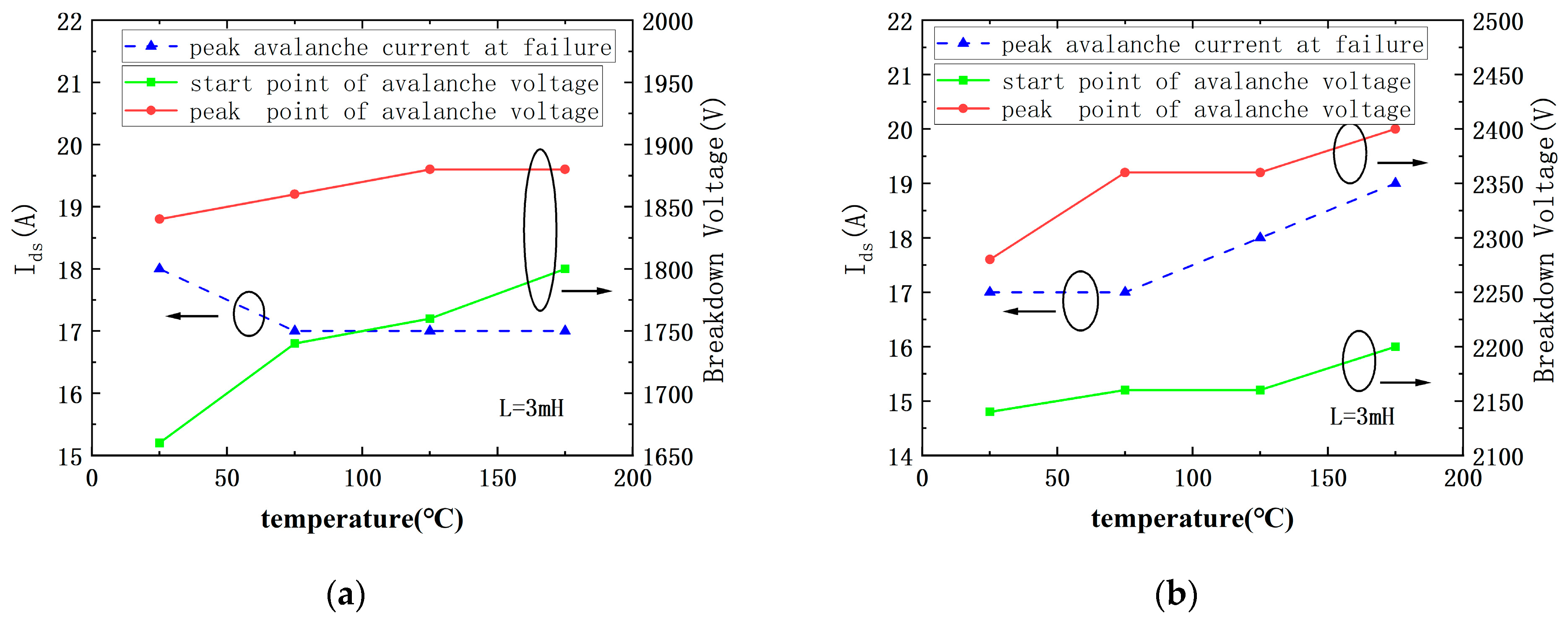
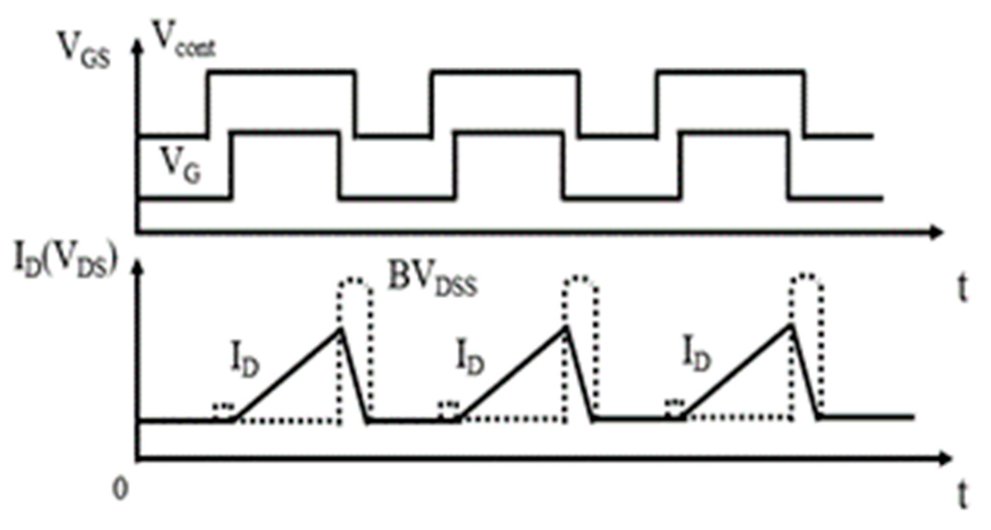
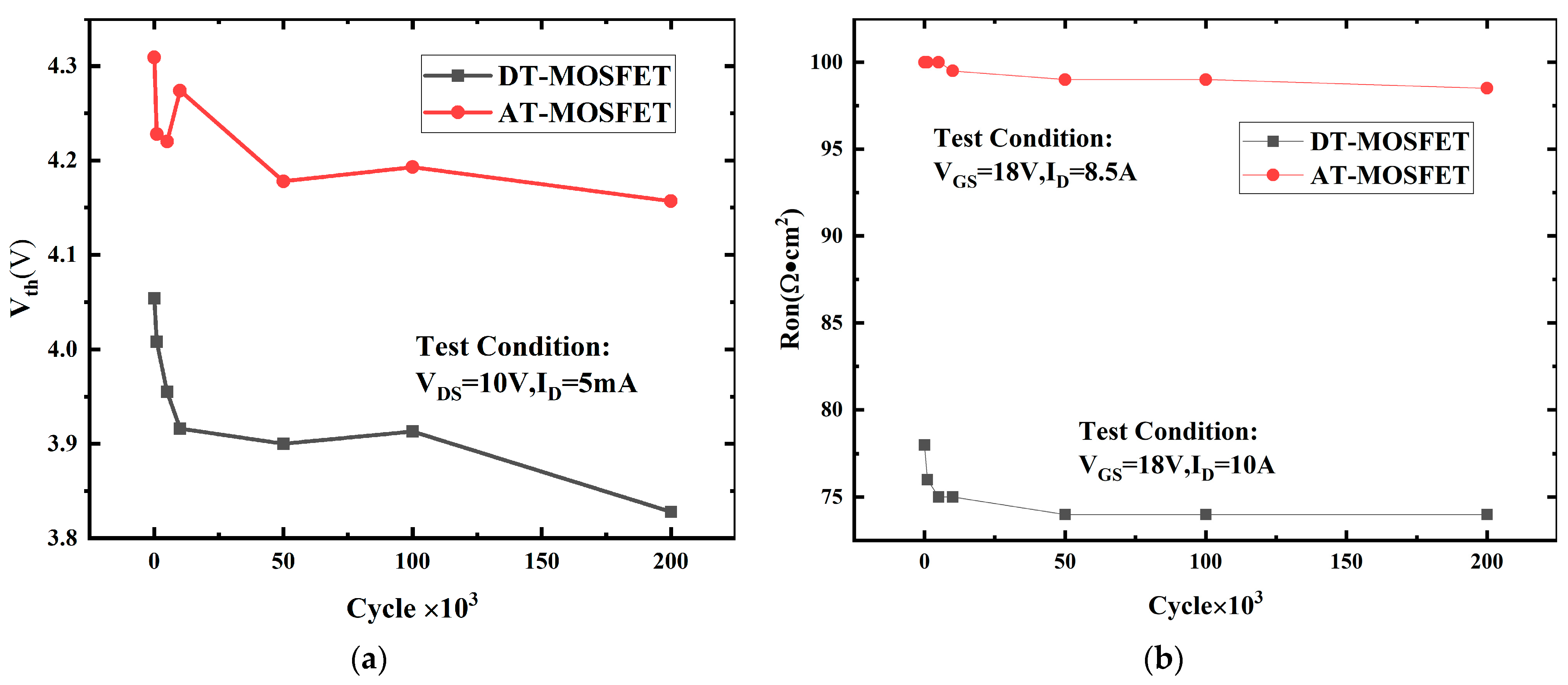
3.2. Repetitive Avalanche Stress

Figure 9 shows the waveforms of a DT-MOSFET and an AT-MOSFET under repetitive avalanche stress. The avalanche energy of each cycle under a repetitive UIS test is set to 20%, with 40% Eav for single UIS. In our experiment, since the experiment phenomena and degradation failure mechanisms are similar to that of a 20% energy ratio, the waveforms and parameter degradations under a 40% energy ratio are not shown here. Vcont and VG are, respectively, the control signals of an IGBT module and gate pulse signal. ID and BVDSS are the inductor current and avalanche voltage, respectively. During the repetitive pulse experiment, a heat sink and fan are used to help with thermal dissipating. The width of the pulse is set to 200 ms under a 20% energy ratio, while the pulse width is 500 ms under a 40% energy ratio. Before our experiment, a pretest confirmed that the pulse width and the heating sink settlement can effectively dissipate the heat from the device.
Figure 10 and Figure 11 give the threshold voltage Vth, on-state resistance Ron, gate leakage current Igss, and forward-voltage of body diode VSD at room temperature versus UIS cycles under a 20% avalanche energy ratio with a load inductance of 3 mH for the AT-MOSFET and for the DT-MOSFET. Vth is tested under VDS = 10 V and ID = 5 mA, while Ron is tested under VGS = 18 V and ID = 10 A. Gate leakage Igss is tested with VGS = 22 V and VDS = 0 V, and Vsd is tested with VGS = 0 V and ISD = 8.5 A. Combined with Figure 10a,b, for the DT-MOSFET, Vth and Ron sharply decrease to 3.9 V and 73 mΩ·cm2, respectively, at the beginning, and then as the cycles increase, the values remain almost unchanged. While, for the AT-MOSFET, these two electrical parameters almost keep constant after repetitive UIS pulses, which indicates that the gate oxide has been well protected by the P+ region in the source of the AT-MOSFET. The strong electrical field under the corner of the gate trench oxide is transferred to the P+ shielding region, thus avoiding the gate oxide dielectric breakdown in advance.
Figure 11a,b present the gate leakage current (Igss) and forward voltage of the body diode (Vsd) of the AT-MOSFET and the DT-MOSFET under a 20% avalanche energy ratio. In Figure 11a,b, for the DT-MOSFET, the Igss increased suddenly after 10 K cycles while the VSD dropped at the beginning. The avalanche has affected both the gate oxide and the body diode of the device. For the AT-MOSFET, the Igss almost remained constant after repetitive UIS pulses, which has been reflected in Figure 10a,b where the Vth and Ron almost remained constant during the cycling test. While in Figure 11b, we can see that UIS cycles had much less of an effect on the VSD of the body diode.

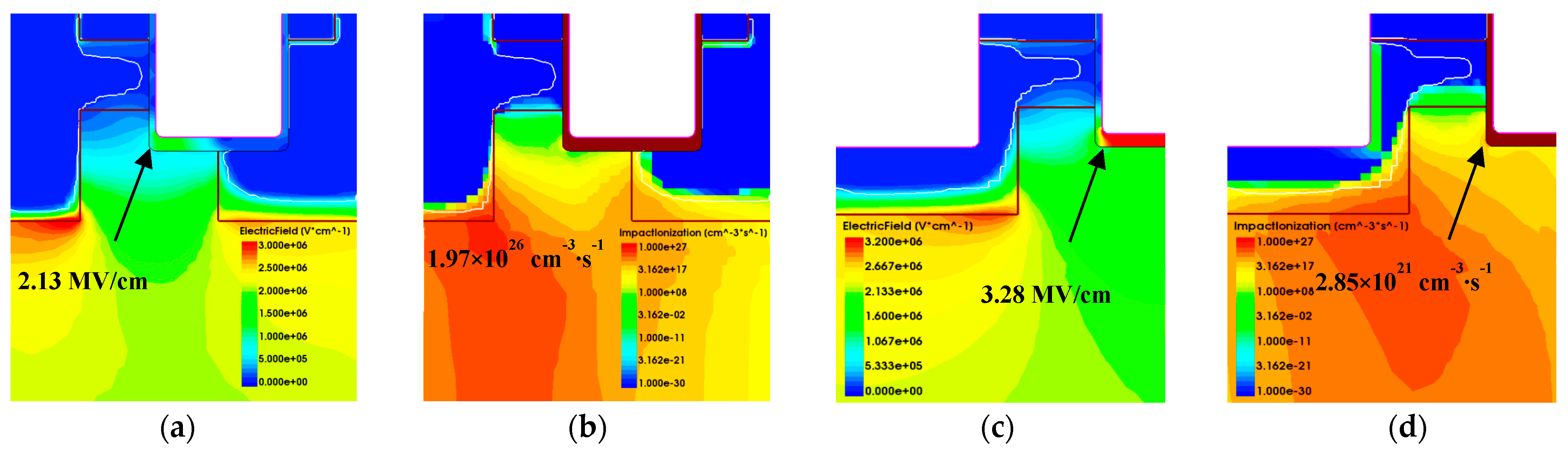
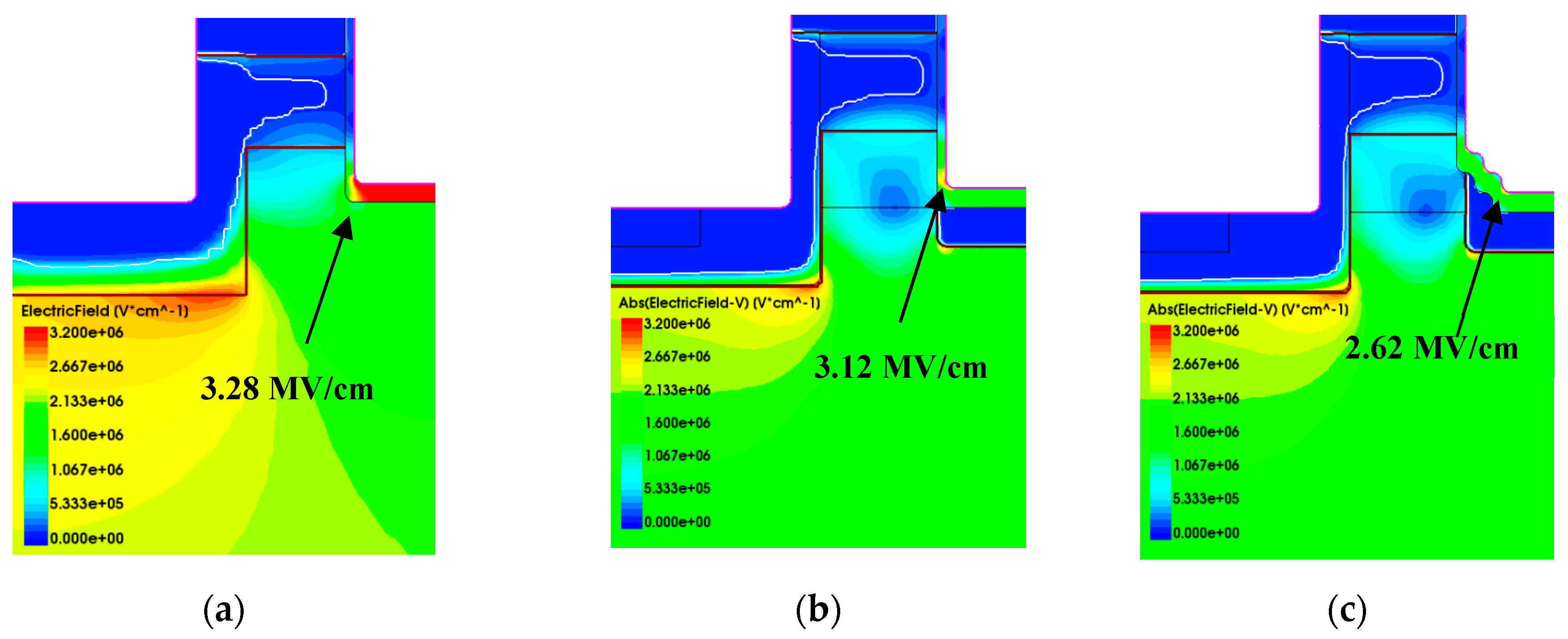
3.3. TCAD Simulation under Repetitive UIS Stress

Figure 12 gives the electrical field profile and impaction ionization (I.I) of the AT-MOSFET and the DT-MOSFET under a 20% avalanche energy ratio with a load inductor of 3 mH. The gate conduction time was set to 500 us and 400 us, respectively. Sentaurus TCAD mixed-mode simulation with coupled electro-thermal conditions was used to investigate the avalanche failure mechanism under repetitive UIS stress. For the AT-MOSFET, the thickness and doping concentration of the drift region were set at 10 μm and 1.2 × 1015 cm−3, respectively. The thickness of the gate oxide at the trench sidewalls and trench bottom was set at 60 nm and 100 nm, respectively. The channel length was 0.5 um with P-type doping 1 × 1017 cm−3. For the DT-MOSFET, the gate trench and source trench were the same size with a width and depth of 1 um. The gate oxide thickness was the same as the AT-MOSFET, and the thickness and doping concentration of the drift region was set to 12 μm and 5.0 × 1017 cm−3, respectively. Physical models, including the avalanche generation “Okuto–Crowell Model”, Shockley–Read–Hall (SRH) recombination, temperature and high electric-field-dependent carrier mobility, incomplete ionization, thermodynamics model, and temperature-dependent intrinsic carrier density, are taken into consideration in the simulation.
It is found from Figure 12a that the corner electrical field of the oxide trench in the AT-MOSFET is 2.13 MV/cm, and the maximum I.I is located near to the body diode, while the I.I under the bottom of the oxide trench is below the 1017 cm−3∙s−1, which indicates that deep p-wells in the asymmetric trench structure could effectively limit the electric field crowding at the trench bottom and prevent the gate oxide breakdown [24,25]. The VDS maintains 1650 V during avalanche; the maximum lattice temperature obtained by simulation is 515 K. However, for the DT-MOSFET, the electrical field in Figure 12c under the bottom of the oxide trench is 3.28 MV/cm, the maximum I.I is located around the body diode, and because of a lack of P-type shielding, the I.I can reach up to 1021 cm−3∙s−1. Under the collective effects of the high electrical field, impact ionization, the holes generated by I.I after obtaining a high level of energy, and being accelerated by avalanche, the electrical field would cross the barrier and be injected into the gate oxide, thus becoming hot carriers in the oxide. The avalanche voltage maintains 2050 V. So, for the AT-MOSFET, the reliability of the body diode could be responsible for the failure of the device, while for the DT-MOSFET, both the gate oxide breakdown and lattice temperature are responsible for the failure of the device.

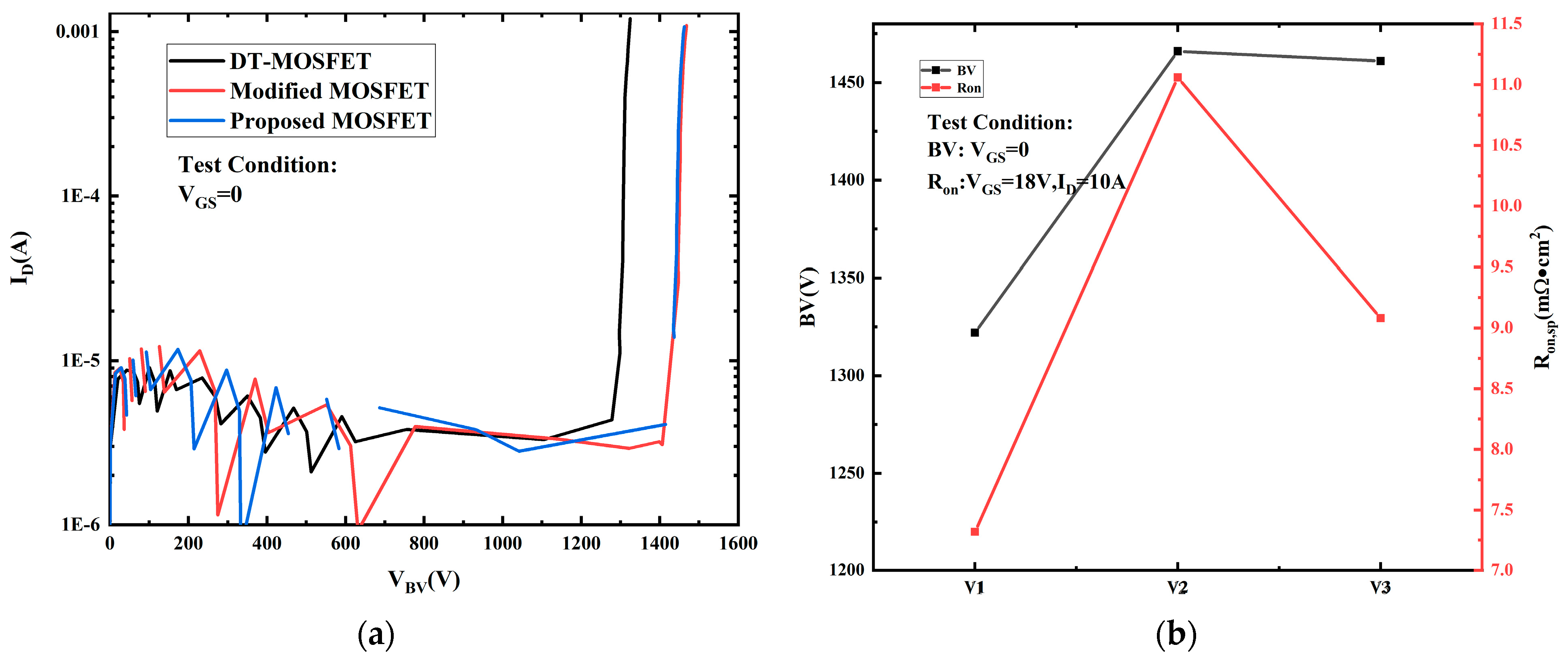
4. Optimization and Simulation

In order to reduce the degradations of the SiC MOSFET, especially the DT-MOSFET under repetitive UIS stress, several improved structures have been proposed, as shown in Figure 13. Based on the DT-MOSFET, a new stepped-oxide structure with p-type shielding under the oxide trench and current spreading layer (CSL) beneath the channel is proposed here in Figure 13c. Correspondingly, its electrical field profiles at its avalanche voltage point is shown in Figure 14a–c. Figure 14a gives the electrical field profile of conventional structure, Figure 14b gives electrical field profile of modified DT-MOSFET and Figure 14c gives electrical field profile of the proposed DT-MOSFET.
Figure 13a depicts a conventional DT-MOSFET. In Figure 13b, a heavy P-type dopant shielding layer is added under the oxide trench to avoid the oxide breakdown in advance. However, P-type shielding will form JFET resistance in conjunction with the P-Well region and lead to an increase in Ron. In order to resolve this problem, a layer of N-type current spreading is added under the channel. Simulation results have shown that, at avalanche voltage working conditions, the horizontal electrical field beneath the oxide trench could be released; however, at the corner of the oxide trench there is still a high electrical field that exits around 3.12 MV/cm which is shown in Figure 14b. Then, in Figure 13c, a stepped-oxide structure with p-type shielding under the oxide trench and CSL beneath the channel is proposed. The corner of the oxide trench is removed with the substitution of the stepped-oxide corner and is protected by a P-type shielding layer. The electrical field at the corner of the oxide trench is reduced to 2.62 MV/cm which is shown in Figure 14c and benefits from the P-type shielding and collective CSL effect.
Figure 15 gives the blocking characteristics, VBV and Ron, of these three structures. Compared with the conventional DT-MOSFET and modified MOSFET, the Ron of the proposed structure decreased about 17.9% with an almost constant breakdown voltage. The breakdown voltage increased from 1320 V to 1460 V, equivalent to about a 10.6% increase.
Figure 16 presents the suggested feasible processing flow of the proposed stepped-oxide structure with p-type shielding and CSL. Initial P-well/CSL/N-drift/N+substrate is choosen as our substrate. The whole processing flows are totally 12 steps. In real processing flow, extra mask could be added between step (g) and step (h) according to the depth and concentration of P-shield region/P+ region.

5. Conclusions

The degradation mechanisms and failure analysis of SiC power MOSFETs under single- and repetitive-frequency UIS characteristics are investigated in this work by experiment and simulation. Previous research has shown that, compared with inductive load, ambient temperature has less influence on the EAV of DUTs. For asymmetric trench devices, avalanche withstanding capability slightly decreases with increasing temperature, while for dual trench devices, avalanche withstanding capability slightly increases with increasing temperature. Under a repetitive UIS test, for an AT-MOSFET with a 20% avalanche energy ratio, Vth and Ron decreased about 3.4% and 2%, respectively, and Cgd increased by 16.7% while the gate oxide remained stable, which indicates that the degradation of devices could be caused by the increase in interface states due to impact ionization. For the DT-MOSFET, Vth and Ron decreased by about 5.4% and 5.1%, respectively, under the same avalanche energy ratio. The gate leakage current Igss is 7 nA, which will increase with a higher avalanche energy ratio. Thus, the degradation of DT-MOSFETs under repetitive pulse is attributed to the hot carrier that is injected into the oxide, leading to the increase in gate leakage current and damage to the gate oxide.
Furthermore, I.I and the electrical field profile at the avalanche state obtained by simulation have shown that the I.I under the oxide trench of the DT-MOSFET will be higher than that of the AT-MOSFET, which further proves that the gate oxide of the DT-MOSFET could be damaged more by electro-thermal stress than the AT-MOSFET.
Additionally, failed devices were decapsulated to verify the location of the failure point and further confirmed the consistencies between the simulation and the experiment. Finally, a new type of stepped-oxide vertical power DT MOSFET with P-type shielding and current spread layers, along with its feasible process flow, is proposed for the improvement of gate dielectric reliability. Compared with DT-MOSFETs, Ron could be decreased by 17.9% with almost the same avalanche voltage ratio.

Author Contributions

Writing—original draft preparation, L.L.; writing—review and editing, J.G.; software, Y.S.; validation, K.Z.; formal analysis, G.L. All authors have read and agreed to the published version of the manuscript.

Funding

This research received no external funding.

Data Availability Statement

Data is contained within the article.

Conflicts of Interest

The authors declare no conflict of interest.

References

  1. Feil, M.W.; Waschneck, K.; Reisinger, H.; Berens, J.; Aichinger, T.; Prigann, S.; Pobegen, G.; Salmen, P.; Rescher, G.; Waldhoer, D.; et al. Gate Switching Instability in Silicon Carbide MOSFETs—Part I: Experimental. IEEE Trans. Electron Devices 2024. [Google Scholar] [CrossRef]
  2. Wang, H.; Lai, P.; Islam, M.Z.; Hasan, A.S.; Di Mauro, A.; Russell, R.; Feng, Z.; Chen, K.; Faruque, A.; White, T.; et al. A review of silicon carbide CMOS technology for harsh environments. Mater. Sci. Semicond. Process. 2024, 178, 108422. [Google Scholar] [CrossRef]
  3. Grome, C.A.; Ji, W. A Brief Review of Single-Event Burnout Failure Mechanisms and Design Tolerances of Silicon Carbide Power MOSFETs. Electronics 2024, 13, 1414. [Google Scholar] [CrossRef]
  4. Liu, T.; Ning, R.; Wong, T.T.Y.; Shen, Z.J. Equivalent circuit models and model validation of SiC MOSFET oscillation phenomenon. In Proceedings of the 2016 IEEE Energy Conversion Congress and Exposition (ECCE), Milwaukee, WI, USA, 18–22 September 2016; pp. 1–8. [Google Scholar]
  5. Schleisser, D.; Ahlers, D.; Eicher, M.; Pürschel, M. Repetitive avalanche of automotive MOSFETs. In Proceedings of the 15th European Conference on Power Electronics and Applications (EPE), Lille, France, 2–6 September 2013; pp. 1–7. [Google Scholar]
  6. Chou, W.; Kempitiya, A.; Vodyakho, O. Reduction of Power Losses of SiC MOSFET Based Power Modules in Automotive Traction Inverter Applications. In Proceedings of the IEEE Transportation Electrification Conference and Expo (ITEC), Long Beach, CA, USA, 13–15 June 2018; pp. 1035–1038. [Google Scholar]
  7. Qi, J.; Yang, X.; Li, X.; Chen, W.; Long, T.; Tian, K.; Hou, X.; Wang, X. Comprehensive Assessment of Avalanche Operating Boundary of SiC Planar/Trench MOSFET in Cryogenic Applications. IEEE Trans. Power Electron. 2021, 36, 6954–6966. [Google Scholar] [CrossRef]
  8. Fu, H.; Wei, J.; Liu, S.; Wu, W.; Sun, W. Repetitive-avalanche-induced Electrical Degradation and Optimization for 1.2 kV 4H-SiC MOSFETs. In Proceedings of the IEEE 26th International Symposium on Physical and Failure Analysis of Integrated Circuits (IPFA), Hangzhou, China, 2–5 July 2019; pp. 1–4. [Google Scholar]
  9. Liu, S.; Gu, C.; Wei, J.; Qian, Q.; Sun, W.; Huang, A.Q. Repetitive Unclamped-Inductive-Switching-Induced Electrical Parameters Degradations and Simulation Optimizations for 4H-SiC MOSFETs. IEEE Trans. Electron Devices 2016, 63, 4331–4338. [Google Scholar] [CrossRef]
  10. Fayyaz, A.; Castellazzi, A.; Romano, G.; Riccio, M.; Irace, A.; Urresti, J.; Wright, N. UIS failure mechanism of SiC power MOSFETs. In Proceedings of the IEEE 4th Workshop on Wide Bandgap Power Devices and Applications (WiPDA), Fayetteville, AR, USA, 7–9 November 2016; pp. 118–122. [Google Scholar]
  11. Gao, Z.; Guo, Q.; Ren, N.; Sheng, K. Experimental Investigation on Failure Mechanism of SiC Power MOSFETs under Single Pulse Avalanche Stress. In Proceedings of the IEEE Workshop on Wide Bandgap Power Devices and Applications in Asia (WiPDA Asia), Suita, Japan, 23–25 September 2020; pp. 1–5. [Google Scholar]
  12. Chen, H.; Wang, J.; Dong, R.; Yao, J.; Liang, S. Investigation on Single Pulse Avalanche Failure of 3.3 kV planar-SiC power MOSFETs. In Proceedings of the IEEE PELS Students and Young Professionals Symposium (SYPS), Shanghai, China, 27–29 August 2023; pp. 1–5. [Google Scholar]
  13. Ren, N.; Wang, K.L.; Wu, J.; Xu, H.; Sheng, K. Failure Mechanism Analysis of SiC MOSFETs in Unclamped Inductive Switching Conditions. In Proceedings of the 31st International Symposium on Power Semiconductor Devices and ICs (ISPSD), Shanghai, China, 19–23 May 2019; pp. 183–186. [Google Scholar]
  14. Kumar, A.; Parashar, S.; Baliga, J.; Bhattacharya, S. Single shot avalanche energy characterization of 10 kV, 10A 4H-SiC MOSFETs. In Proceedings of the IEEE Applied Power Electronics Conference and Exposition (APEC), San Antonio, TX, USA, 4–8 March 2018; pp. 2737–2742. [Google Scholar]
  15. Kelley, M.D.; Pushpakaran, B.N.; Bayne, S.B. Single-Pulse Avalanche Mode Robustness of Commercial 1200 V/80 mΩ SiC MOSFETs. IEEE Trans. Power Electron. 2017, 32, 6405–6415. [Google Scholar] [CrossRef]
  16. Dchar, I.; Zolkos, M.; Buttay, C.; Morel, H. Robustness of SiC MOSFET under avalanche conditions. In Proceedings of the IEEE Applied Power Electronics Conference and Exposition (APEC), Tampa, FL, USA, 26–30 March 2017; pp. 2263–2268. [Google Scholar]
  17. Li, K.; Sun, P.; Wu, S.; He, Z. Experimental Investigation on Avalanche Robustness of SiC MOSFETs in the Aging Process. In Proceedings of the 4th International Conference on Power and Energy Technology (ICPET), Beijing, China, 28–31 July 2022; pp. 1227–1231. [Google Scholar]
  18. Bai, Z.; Tang, X.; Xie, S.; He, Y.; Yuan, H.; Song, Q.; Zhang, Y. Investigation on Single Pulse Avalanche Failure of 1200-V SiC MOSFETs via Optimized Thermoelectric Simulation. IEEE Trans. Electron Devices 2021, 68, 1168–1175. [Google Scholar] [CrossRef]
  19. Wang, J.; Jiang, X. Review and analysis of SiC MOSFETs’ ruggedness and reliability. IET Power Electron. 2020, 13, 445–455. [Google Scholar] [CrossRef]
  20. Wei, J.; Liu, S.; Yang, L.; Tang, L.; Lou, R.; Li, T.; Fang, J.; Li, S.; Zhang, C.; Sun, W. Investigations on the Degradations of Double-Trench SiC Power MOSFETs under Repetitive Avalanche Stress. IEEE Trans. Electron Devices 2019, 66, 546–552. [Google Scholar] [CrossRef]
  21. Wei, J.; Wei, Z.; Fu, H.; Cao, J.; Wu, T.; Sun, J.; Zhu, X.; Li, S.; Zhang, L.; Liu, S.; et al. Review on the Reliability Mechanisms of SiC Power MOSFETs: A Comparison between Planar-Gate and Trench-Gate Structures. IEEE Trans. Power Electron. 2023, 38, 8990–9005. [Google Scholar] [CrossRef]
  22. Yao, K.; Yano, H.; Iwamuro, N. Impact of Negative Gate Bias and Inductive Load on the Single-Pulse Avalanche Capability of 1200-V SiC Trench MOSFETs. IEEE Trans. Electron Devices 2022, 69, 637–643. [Google Scholar] [CrossRef]
  23. Tsuji, T.; Iwamuro, N. An investigation of avalanche ruggedness and failure mechanisms of 4H SiC trench MOSFETs in unclamped inductive switching by varying load inductances over a wide range. Jpn. J. Appl. Phys. 2023, 62, 041001. [Google Scholar] [CrossRef]
  24. Hu, J.; Alatise, O.; Gonzalez, J.A.O.; Bonyadi, R.; Alexakis, P.; Ran, L.; Mawby, P. Robustness and Balancing of Parallel-Connected Power Devices: SiC Versus CoolMOS. IEEE Trans. Ind. Electron. 2016, 63, 2092–2102. [Google Scholar] [CrossRef]
  25. Deng, X.; Zhu, H.; Li, X.; Tong, X.; Gao, S.; Wen, Y.; Bai, S.; Chen, W.; Zhou, K.; Zhang, B. Investigation and Failure Mode of Asymmetric and Double Trench SiC MOSFETs under Avalanche Conditions. IEEE Trans. Power Electron. 2020, 35, 8524–8531. [Google Scholar] [CrossRef]
Figure 1. Cross-section of 4H-SiC trench MOSFET: (a) DT-MOSFET; (b) AT-MOSFET.
Micromachines 15 00772 g001
Figure 2. UIS test circuit of 4H-SiC power MOSFET: (a) Schematic circuit of UIS test; (b) wave form diagram of tested circuit; (c) UIS test setup.
Micromachines 15 00772 g002
Figure 3. Single-pulse UIS waveforms with load inductor of 3 mH at the last test before failure: (a) DT-MOSFET; (b) AT-MOSFET.
Micromachines 15 00772 g003
Figure 4. Single-pulse UIS waveforms with load inductor of 3 mH at failure: (a) DT-MOSFET; (b) AT-MOSFET.
Micromachines 15 00772 g004
Figure 5. EAV and tAV versus ton for AT-MOSFETs (a) and DT-MOSFETs (b) under different ambient temperatures with inductor load of 3 mH.
Micromachines 15 00772 g005
Figure 6. EAV and tAV versus ambient temperature of AT-MOSFETs (a) and DT-MOSFETs (b).
Micromachines 15 00772 g006
Figure 7. Ipeak, BVst, and Vpeak of DT-MOSFETs (b) and AT-MOSFETs (a) versus ambient temperature at failure with load inductor of 3 mH.
Micromachines 15 00772 g007
Figure 8. Decapsulation image of AT-MOSFET (a), decapsulation of DT-MOS and failure point at 25 °C (b), and decapsulation of DT-MOS and failure point at 175 °C (c).
Micromachines 15 00772 g008
Figure 9. Repetitive avalanche UIS test waveform diagrams.
Micromachines 15 00772 g009
Figure 10. Vth versus cycles (a) and Ron versus cycles (b), Vth and Ron of AT-MOSFET (0.46 × 0.2 = 0.09 J, L = 3 mH) and DT-MOSFET (0.19 × 0.2 = 0.038 J, L = 3 mH) versus cycles under 20% avalanche energy ratio.
Micromachines 15 00772 g010
Figure 11. Igss versus cycles (a) and Vsd versus cycles (b), gate leakage current (Igss) and forward voltage of body diode (Vsd) of AT-MOSFET and DT-MOSFET under 20% avalanche energy ratio.
Micromachines 15 00772 g011
Figure 12. Electrical field of AT-MOSFET (a), I.I of AT-MOSFET (b), electrical field of DT-MOSFET (c), I.I of DT-MOSFET (d), and electrical field profile and impaction ionization (I.I) of AT-MOSFET and DT-MOSFET under 20% avalanche energy ratio.
Micromachines 15 00772 g012
Figure 13. Cross-section comparison of three devices: (a) conventional DT-MOSFET, (b) modified DT-MOSFET, and (c) proposed DT-MOSFET.
Micromachines 15 00772 g013
Figure 14. Electrical field profile in different structures (obtained at avalanche points): (a) conventional DT-MOSFET, (b) modified DT-MOSFET, and (c) proposed DT-MOSFET.
Micromachines 15 00772 g014
Figure 15. Blocking characteristics and Ron variation of these three devices (a) Blocking characteristics, (b) Ron variation of these three devices.
Micromachines 15 00772 g015
Figure 16. Feasible process flow of proposed DT-MOSFET in Figure 13c.
Micromachines 15 00772 g016
Table 1. Comparison of EAV, IDS,MAX, VDSMAX, and tAV tested under single UIS pulse with different inductor loads at room temperature.
ParametersDT-MOSFETAT-MOSFET
1 mH3 mH10 mH1 mH3 mH10 mH
EAV0.19 J0.47 J0.57 J0.46 J0.53 J0.67 J
IDS,max19 A18 A10.5 A30 A19 A11 A
VDS,Max2240 V2280 V2320 V1840 V1820 V1800 V
tAV3.13 μs30.45 ns49.35 μs15.23 μs18.45 μs40 μs
Disclaimer/Publisher’s Note: The statements, opinions and data contained in all publications are solely those of the individual author(s) and contributor(s) and not of MDPI and/or the editor(s). MDPI and/or the editor(s) disclaim responsibility for any injury to people or property resulting from any ideas, methods, instructions or products referred to in the content.

