Abstract
Electrical isolation devices are essential components for safeguarding the reliability of electronic systems under harsh conditions. Digital isolators are widely used in low-power circuits due to their high immunity to disturbances. In this paper, a capacitive digital isolator for high-efficiency power supply scenarios is proposed with a high common-mode transient immunity (CMTI) and high data transmission rate. The on–off keying (OOK) modulation technique is used to ensure a high speed and accurate signal transmission. A fully integrated high-voltage level-shift driver with an ns-scale delay is proposed for increasing the drive capacity. Post-simulation results in Cadence IC 6.1.7 with the standard 0.18 μm CMOS process show that the proposed architecture achieves a 25 Mbps data transmission rate and 15 ns typical propagation delay with output peak currents of 2 A/4 A, respectively. Meanwhile, a CMTI of more than 150 kV/μs is realized.
1. Introduction
Digital isolators protect systems and users from potentially hazardous voltages in high-voltage environments [1,2,3]. Digital isolators based on the CMOS process are widely used in various applications due to their small size and high reliability [4,5]. Digital isolators with common-mode transient immunity (CMTI) become basic devices in low-power applications. The development of digital isolators is directed towards two directions, reducing cost and optimizing performance [6]. Inductive coupling and capacitive coupling are two common forms of isolation in CMOS-based digital isolators.
Isolators based on inductive coupling utilize their self-inductive properties to realize long-distance data transfer [7]. However, transformers typically require significant space, and even require another mould for placement. The coil diameter of the transformer in [8] is as high as 230 μm, even requiring silicon-based post-processing techniques, which leads to increased costs. Pulse modulation technique is used in [9] to address the area and power consumption concerns. However, a GHz-range signal is generated, which affects noise immunity. Finally, the CMTI of [9] is limited to 25 kV/µs. A transformer isolator based on time multiplexing is presented by [10], which uses a 0.1 mm-thick isolation coefficient as the dielectric, but only achieved a 100 kV/µs CMTI. In contrast, capacitive isolators utilize SiO2 as the isolation dielectric material, whose field strength is about 400–500 Vrms /µm at room temperature. In a standard 0.18 μm CMOS process, a 5 µm thickness between Metal 1 and Metal 4 can theoretically achieve an isolation withstanding capacity of 2.5 kV. Compared to inductive isolation, capacitive isolation operates on electric fields alone and can be used without interference from the magnetic field of the surrounding MRI equipment. Additionally, the robustness under fast transient changes makes it more advantageous [11]. Due to the higher data rate, lower latency, and reduced cost, the capacitive isolator has gradually replaced the traditional magnetic coupler isolator in many applications.
The modulation methods of digital isolators can be broadly categorized into edge modulation and on–off keying (OOK) modulation. The way of encoding using the edge of the signal is easily affected by noise interference. In contrast, OOK modulation technology can significantly improve communication efficiency, and reduce transmission distance and transmission loss, while ensuring communication reliability.
Most current commercial isolation products have a narrow supply voltage range. For example, the capacitive digital isolator presented in [12] offers ultra-low power dissipation, but the typical application is a loop-powered field transmitter from 4 mA to 20 mA. An isolator that supports high transmission rates from DC to 50 Mbps per channel was proposed in [13], but the output current is only 4 mA. Moreover, most products have independent isolated channels, which makes it difficult to use them flexibly in different scenarios. In addition, the common-mode rejection (CMR) of many commercial products is limited to 100 kV/μs [14,15,16].
This paper proposes a dual-channel configurable capacitively coupled digital isolation driver based on OOK modulation. The transmitter (TX) die and receiver (RX) die are configured with a capacitive isolation barrier, and the two capacitors are connected back-to-back, which doubles the channel breakdown voltage and improves the isolation capability of the chip. Each channel is equipped with an independent shutdown pin. An external pin is designed to enable a programmable dead time function. With an input voltage range of 3.3 V to 5 V and an operating voltage of up to 20 V on the output side, it is suitable for connecting digital and analogue controllers. The proposed isolated driver architecture provides an up to 25 Mbps data rate and an up to 2 A/4 A output current with a typical propagation delay of 14.5 ns, while achieving an excellent CMTI capability of more than 150 kV/µs.
2. Materials and Methods
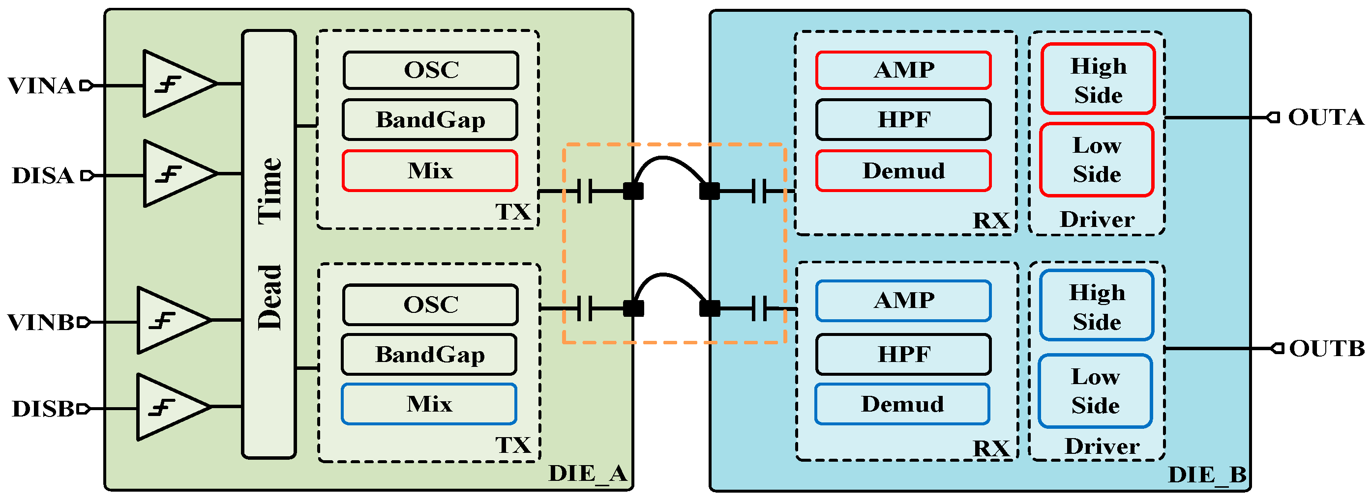
Figure 1 shows the overall architecture of the proposed digital isolated driver. The input side and output side are placed on separate substrates and packaged in a single package. Two metal–oxide–metal capacitors are used as isolation capacitors to match the fully differential transmission mode used in the TX section. The sectional schematic of the integrated isolation capacitor used is shown in Figure 2. The size of this isolation capacitor is determined by the area of the top and bottom pole plates and the distance between the plates. In 0.18 μm CMOS five-layer metal interconnect process, Metal 1 is used as the lower plate, while Metal 5 is used as the upper plate, and a silicon dioxide dielectric with a pitch of 4.8 μm is used as the isolation barrier, with a capacitor of 50 fF each. With two capacitors placed consecutively between TX and RX, a reinforced isolation level of 4.2 kVRMS can eventually be achieved.

Figure 1.
Overall architecture of the proposed digital isolated driver.
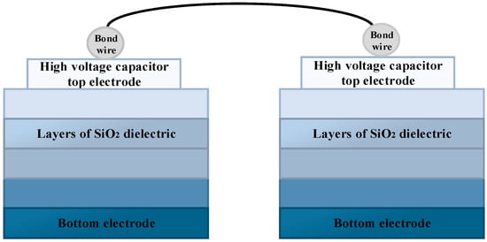
Figure 2.
Cross-section of high-voltage isolation capacitor.
The TX on input side include a Schmitt trigger for filtering, an internal oscillator (OSC) to generate the carrier signal, and a mixer to modulate the origin signal. The RX on the output side consists of a high-pass filter (HPF), a pre-amplifier, and a demodulator for accurately reconstructing the initial signal with low transmission delay. The output stage is designed as a fully integrated high-voltage level-shifted high-side and low-side driver, in order to minimize the passive device area of the isolator, ultimately providing sufficient drive capability with a 1.2 nF load connected.
The designed isolated driver can be configured as two signal-side drivers or a half-bridge driver with adjustable dead time. Two channels have independent ‘enable control’ pins. The chip operates normally when ports DISA and DISB are connected to a low level, and the outputs are pulled low when connected to a high level. The DT pin is used to control the dead time between two channels. When DT is high, channels operate independently and dead time control function is disabled. When DT is connected with a resistor to ground, the dead time between channels is determined by the magnitude of the external resistor.
2.1. Transmitter
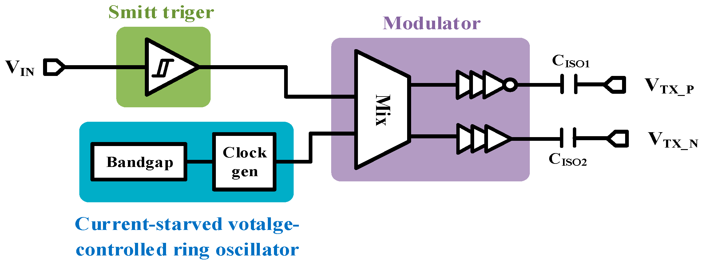
The overall block diagram of the TX is shown in Figure 3. As an important part of the transmitter, the built-in bandgap generates a high-resolution reference voltage that is less disturbed by environmental factors, enabling the whole system to work stably over a wide temperature range [17]. The input signal is first converted from analogue to digital by a Schmitt flip-flop, which shapes the signal and removes noise, enhancing the overall immunity of the circuit. As an implementation of ASK modulation, the analogue multiplier mixes the input signal with the carrier signal by using electronic switches to control the output of the oscillator and turn it off [18]. When the input is high, the output is a high-frequency carrier signal, and, when the input is low, the output is a low signal. The insensitivity of this modulation method to the data transmission rate results in high immunity.
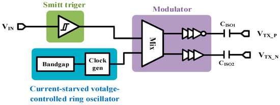
Figure 3.
Block diagram of TX.
The maximum data transmission rate of this design driver is 25 Mbps. According to Nyquist’s sampling theory, the output frequency of the oscillator should be at least twice the frequency of the input signal to avoid aliasing of the output signal [14]. In practice, to achieve higher transmission reliability and stronger immunity to disturbances, the input signal is often made to contain more than five oscillation cycles within the minimum pulse width. On the other hand, to maximize the rate of data transmission, the OSC should be kept oscillating at a high frequency. After considering the above, the oscillator frequency is designed at 200 MHz. We use current-starved voltage-controlled ring oscillator (CSVCRO) structure to reduce the influence of PVT variation [15,16]. A self-biasing circuit is used to control the bias current of the inverter, and the time of charging and discharging the load capacitor is controlled by fixing the bias current to minimize the frequency error caused by PVT variation. Oscillator with CSVCR structure exhibits good robustness, omits additional calibration steps, and simplifies the circuit topology, offering advantages in terms of area and cost savings.
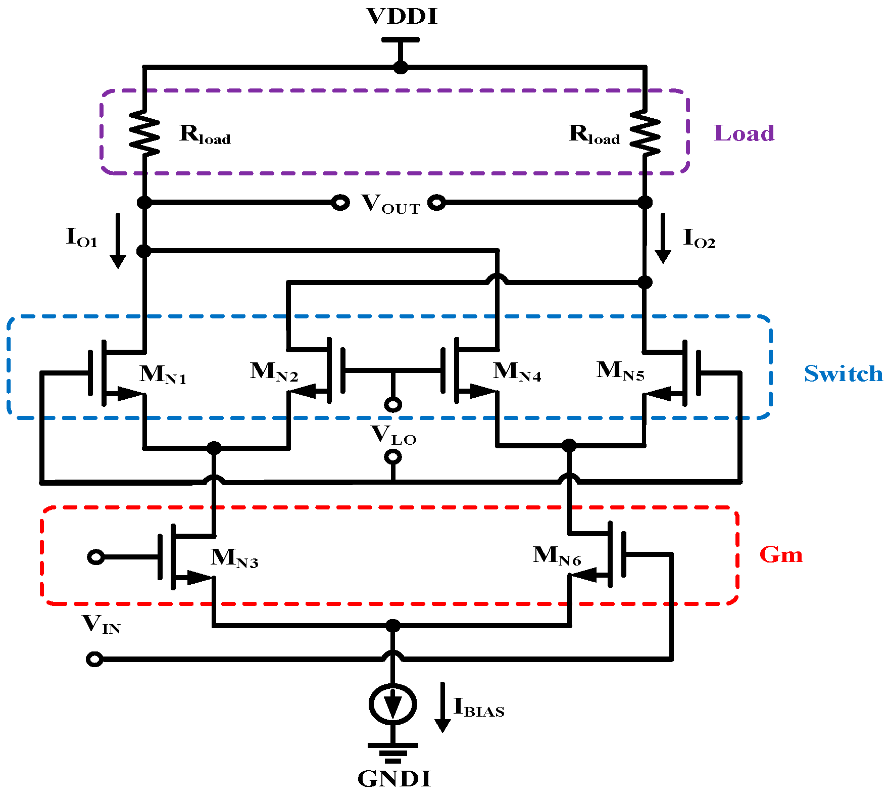
Figure 4 shows the architecture of the Gilbert double-balanced analogue multiplying mixer. The input signal VIN is amplified in the Gm stage, frequency down-converted to a current signal in the switching stage, and then converted to a voltage signal by the output load stage. Compared to single-transistor or single-balanced mixers, the double-balanced mixer offers better isolation between its ports, and the currents of the upper two differential pairs are super-imposed in opposite phases, which cancels out the leakage of the input signal to the mediate frequency port. The conversion efficiency of the multiplying mixer depends only on the input current and current gain. When the input voltage changes, the Gilbert cell form a rapidly responding path to trigger the output.
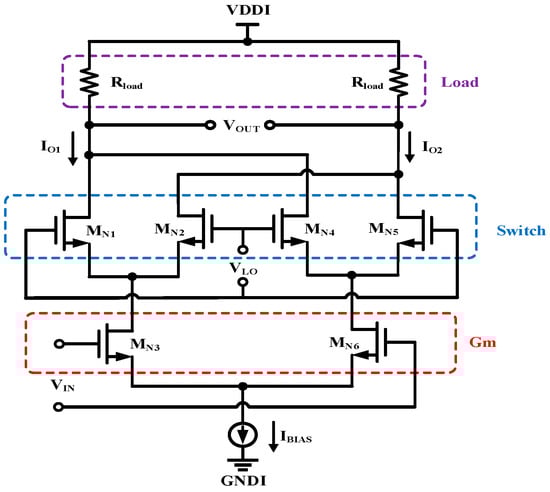
Figure 4.
Double-balanced mixer Gilbert cell.
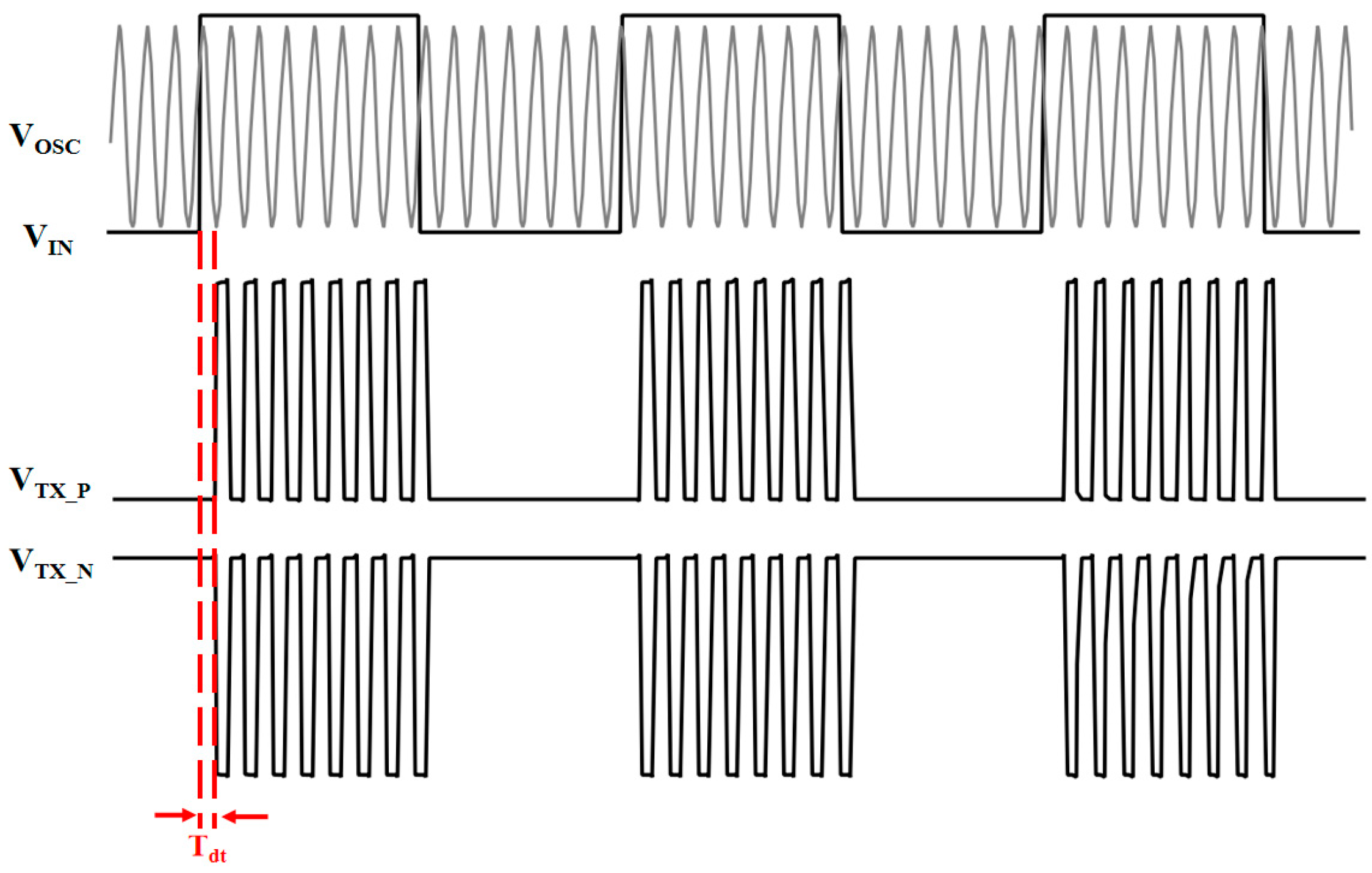
Figure 5 shows the operating waveform diagram of the mixer, where Tdt is its propagation delay. The adopted form of OOK modulation minimizes the overall delay of the TX section.
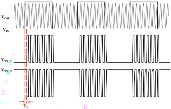
Figure 5.
Diagram of main signal waveforms in TX.
2.2. Receiver
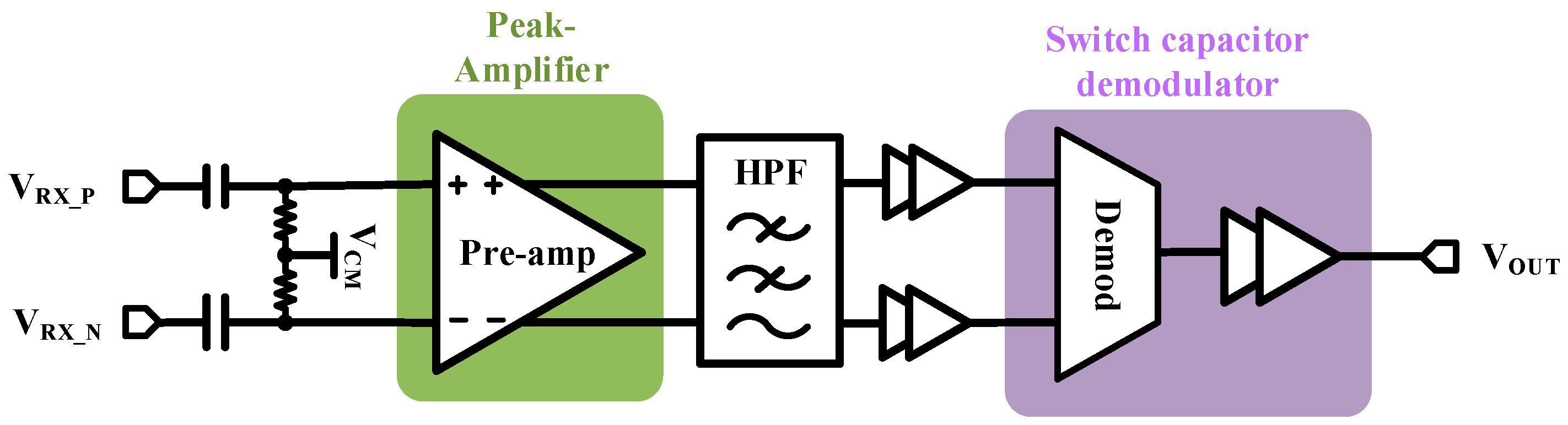
Figure 6 shows the proposed RX structure. The RX should be designed to take into account the DC operating point shift caused by common-mode transient events, and the high-frequency signal should be recovered from which it is attenuated by the isolation capacitors. The pre-amplifier is adopted to amplify the carrier waveform. In addition, it should maintain normal operation during the occurrence of voltage surges. The high-pass filter (HPF) removes the common-mode noise and reduces pre-amplifier offsets. The envelope detector (ED) is used for more efficient demodulation and reconstruction of the initial input signal.
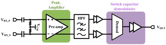
Figure 6.
Block diagram of RX.
The peak gain pre-amplifier and its small-signal model are shown in Figure 7. A wide-bandwidth amplifier without high-impedance nodes is designed to achieve RF-level bandwidth. The fully differential form of dual-in-dual-out (DIDO) is used to suppress low-frequency common-mode signals effectively [19]. For low-frequency inputs, the single-side circuit can be equated to a common-source pole amplifier circuit with a PMOS diode connection as the load, and the gain can be calculated by Equation (1). Therefore, with proper size of M1 and M3, a gain of 1× (or slightly less than 1×) peak amplifier at low frequencies can be achieved.
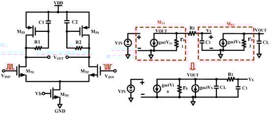
Figure 7.
Peak amplifier diagram and small-signal model.
For high-frequency inputs, R1 and C1 form a low-frequency filtering circuit. In AC small-signal model of the circuit, CL represents the total capacitor from the output node to ground, and ro is equal to ro1//ro2. Collation yields the small-signal gain G(s) of the peak amplifier as:
The peak response gain with bandpass effect can be achieved by selecting the RC value under certain conditions. It is worth noting that, if a narrower passband bandwidth is chosen for better filtering, although it can suppress low-frequency common-mode signals, its gain at the peak will be greatly reduced and the transient response is prone to distortion. Therefore, the choice of frequency bandwidth for the signal amplification region requires a trade-off.
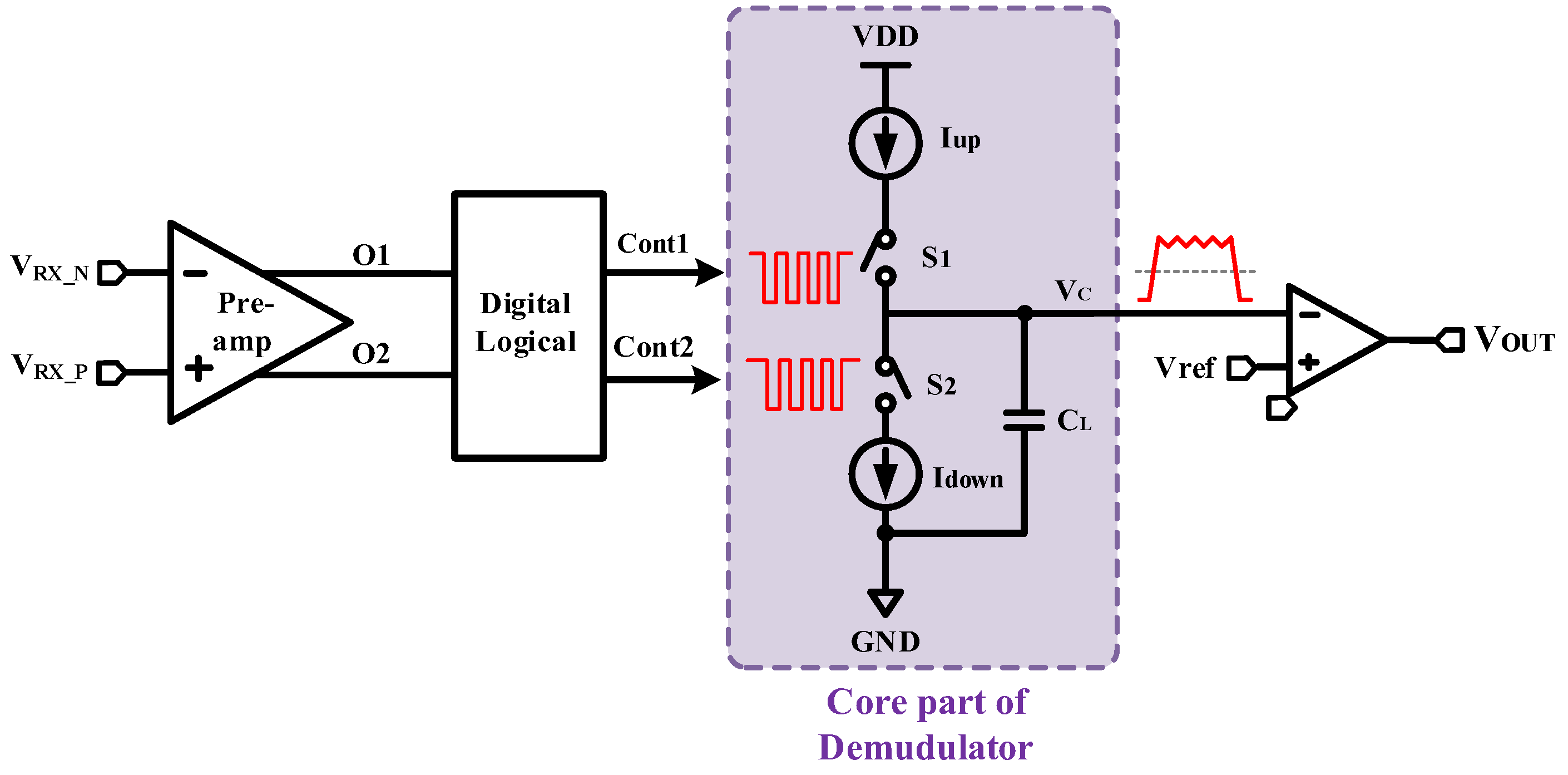
The challenge of the demodulation circuit is to maintain accuracy and efficiently restore the high-frequency output signal to the input signal while maintaining low delay. Figure 8 shows the block diagram of the overall demodulation circuit. The core of the demodulation circuit contains two current sources, two complementary MOS switches, and a 100 fF capacitor. The amplified differential signal is first input to the digital logic unit for signal processing, and obtains two in-phase non-interleaved clock signals as the result, to control the upper and lower MOSFET switches, respectively. Thus, the capacitors were subjected to irregular charging and discharging. The voltage of the upper pole plate of the capacitor is used as the primary demodulation signal, which is input to the negative terminal of the comparator to compare with the reference voltage to obtain the final demodulation signal.

Figure 8.
Basic principle of demodulator.
To achieve better demodulation, certain restrictions on the current magnitude and switch signal are needed. Firstly, a larger charging current and a smaller discharging current are chosen. Then, the capacitor exhibits fast charging and slow discharging, and the primary demodulation signal can be pulled up quickly when the input signal jumps from low to high. Secondly, during the periodic switching process, a smaller leakage current ensures a slow decrease in signal and minimal amplitude during the opening period of the low-side current source. At the same time, a larger pull-up current continuously charges the capacitor during the opening period of the high-side current source, which can maintain a high level of output.
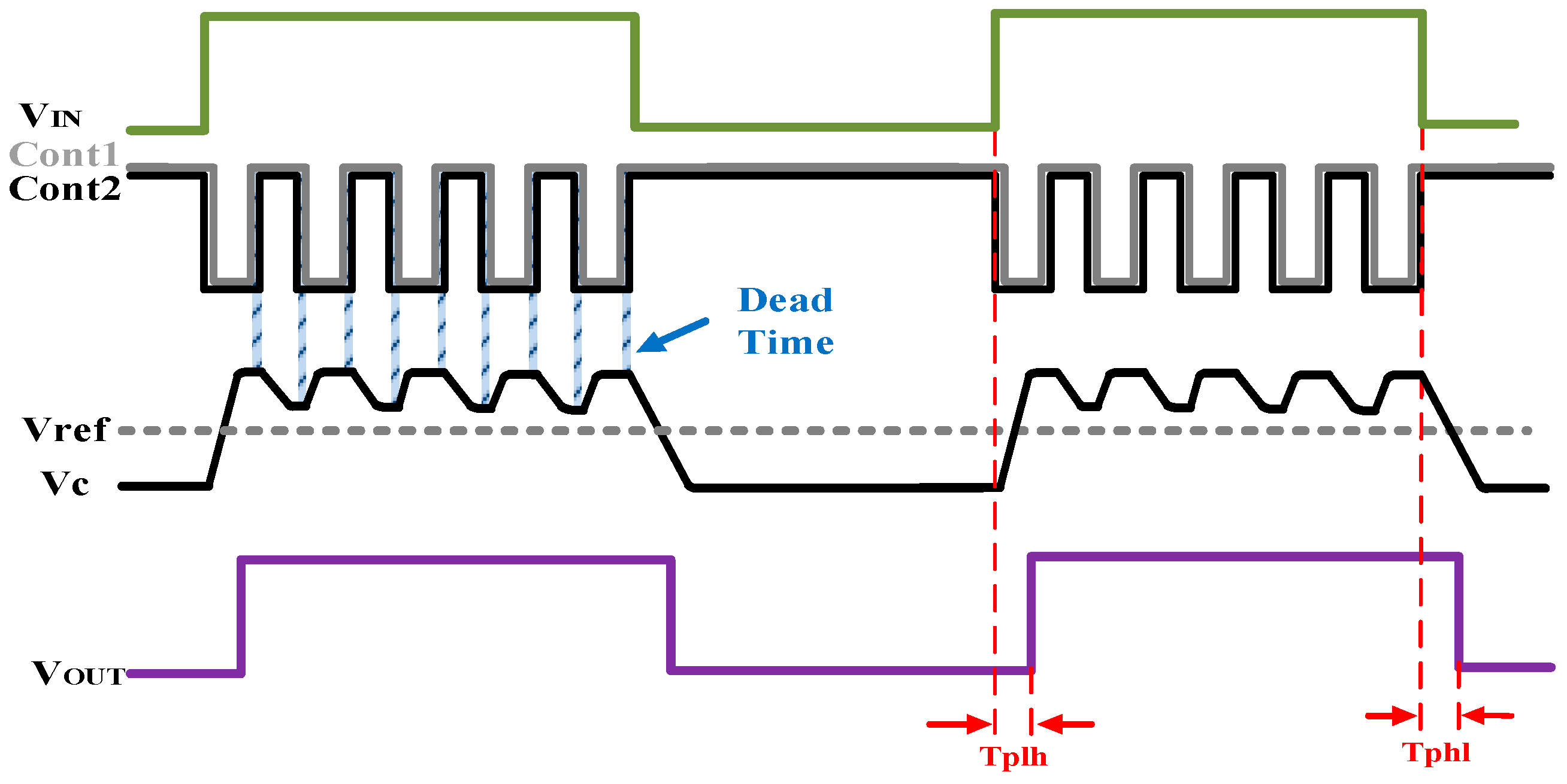
On the other hand, a certain dead time should be set for the two control signals to prevent high-current throughput caused by simultaneous opening of the upper and lower MOS switches. Figure 9 shows the operation waveform of the core demodulation unit. The logical relationship between the upper and lower current source switches S1 and S2 and the input signal VIN should be as follows: during the period when VIN is low, S1 is turned off and S2 is turned on, and the output corresponds to a low level; during the period when VIN is high, S2 is turned off, and then S1 is turned on again after a certain dead time, and so on, repeatedly, alternately. When the input level into the next cycle flipped to a low level, ensure S2 is open after S1 is off. Note that, due to the switch, the single turn-on time is shorter, and the size of the charge–discharge current will have a greater impact on the output waveforms, so it is better to select a higher-resolution current source, such as Cascode structure with high output impedance [20].
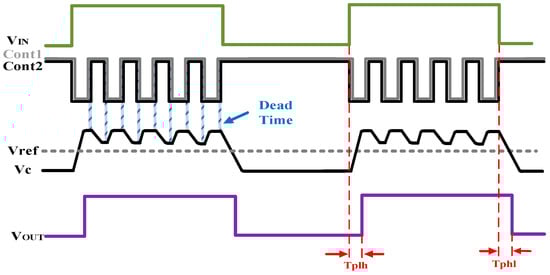
Figure 9.
Diagram of DE operation waveforms.
2.3. Driver
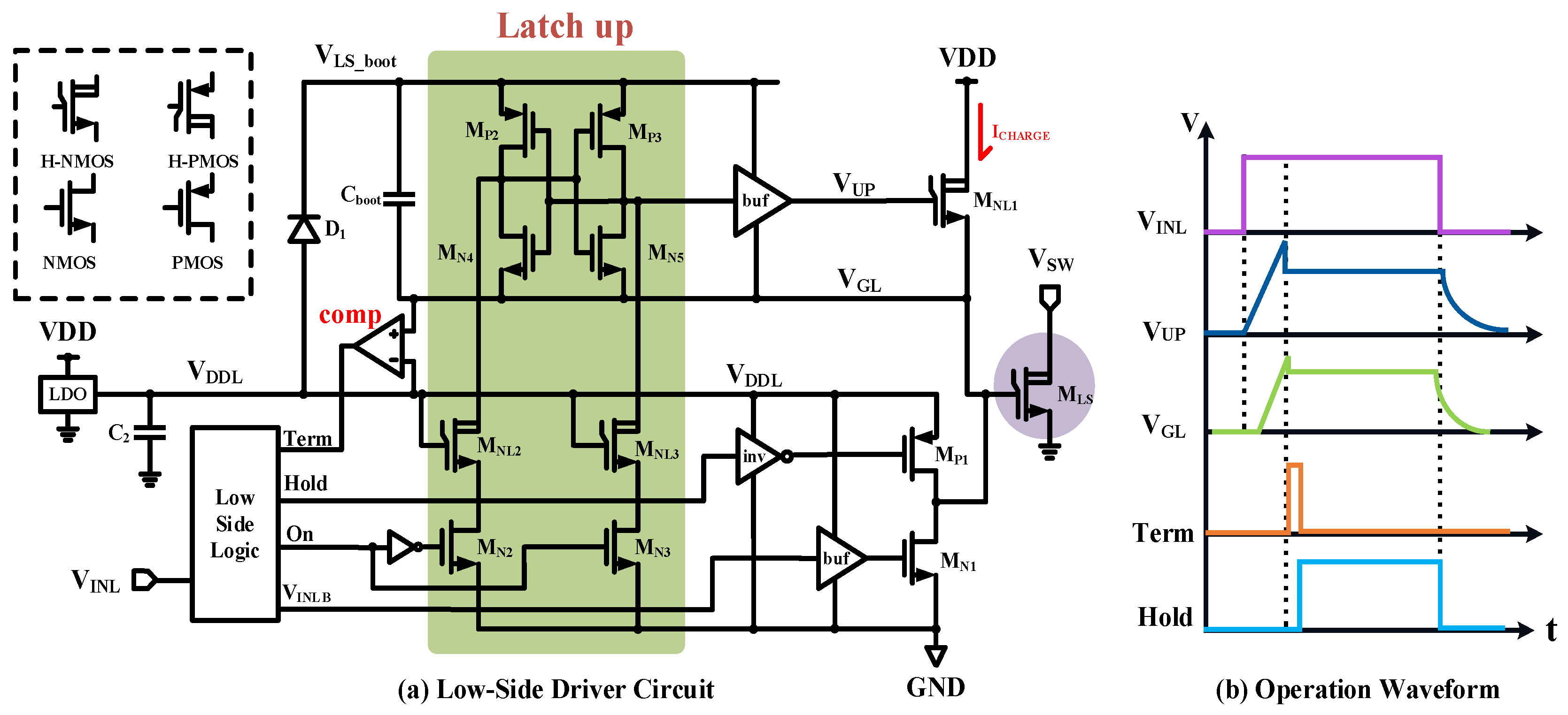
Figure 10 shows the circuit diagram of the high-voltage low-side driver. The built-in LDO with capacitor C2 provides power for the low-voltage domain of the low-side drive. The larger-sized transistor MNL1 and MP1 work sequentially to provide the charging circuit for the power transistor MLS during the turn-on process; MN1 with a buffer provides a discharging circuit for the MLS; MN2~MN5, MNL2~MNL3, and MP2~MP3 comprise the low-side level-shifter. Diode D1 and bootstrap capacitor Cboot are used to implement the lifting of the potential of the floating power supply rails; the comparator detects the gate voltage of MLS to achieve the gate protection function.
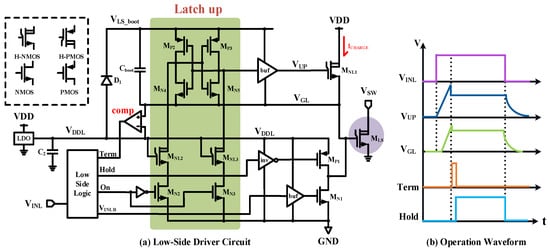
Figure 10.
Proposed low-side driver.
There is a high-voltage level-shifter inside the low-side Driver. If the gate signal of the pull-up transistor MNL1 is supplied from the power rail VDDL, the maximum power device MLS gate drive voltage can only reach VDDL-Vth, which is just suitable for the low-voltage drive applications. To better drive the MLS, a level-shifting circuit utilizing bootstrap capacitor Cboot is designed in order to generate a floating power supply VLS_boot. When the low-side input VINL is low, Cboot is charged by VDD through diode D1, and the voltage difference between the two ends of Cboot is VDD minus the conduction voltage drop of D1. When VINL is flipped high, the gate voltage of MLS is instantly lifted to VDDL; because the voltage across the capacitor cannot change abruptly, VLS_boot will be lifted to 2 times VDDL, thus achieving the level-shifting circuit.
When the input to the low-side driver is low, the discharge current of MLS flows directly into GND through the pull-down switch MN1. When the input is high, the MLS turns on in two stages. Firstly, MNL1 conducts to charge the MLS gate. In this stage, charging current comes from the Drive supply VDD instead of the floating supply rail VDDL, that can eliminate the high-current disturbances on the LDO output supply, thus avoiding the use of off-chip capacitors to maintain the power rails for the low-side drive. When MLS gate voltage is higher than 5 V, the turn-on process turns to gate voltage holding stage. At this point, the output of the comparator is processed by the logic unit into a short-pulse Term to close the gate-charging process to protect the MLS from breakdown. Meanwhile, MP1 is open in order to maintain the gate voltage of MLS with a small pull-up current. The threshold voltage of the comparator should be designed slightly lower than the supply rail VDDL for compensating the comparator’s transmission delay.
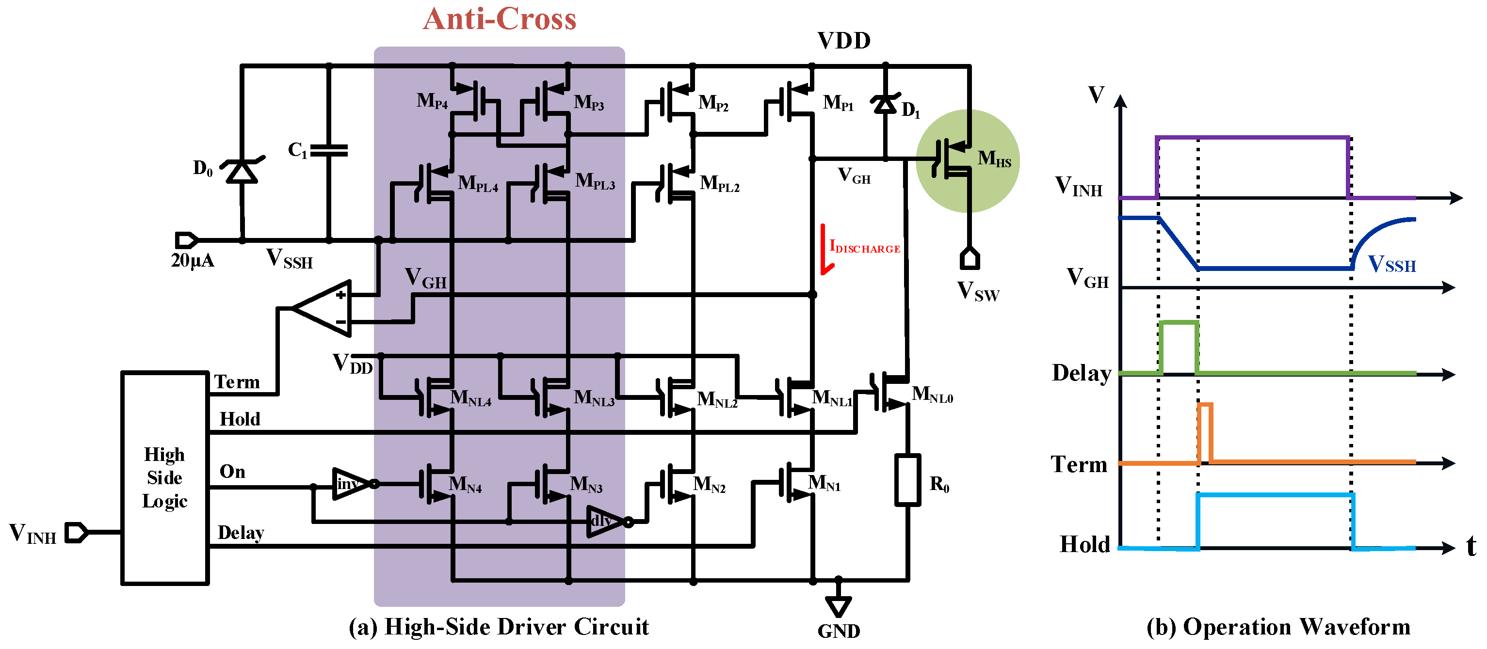
The high-voltage high-side driver is shown as Figure 11, which includes a floating ground rail VSSH generation circuit, level-shift circuit consisting of MN2 to MN4 branches with anti-cross conduction functionality, and a gate protection circuit for the power transistor. The sizes of MP1 that is responsible for pulling up MHS, and MNL1 that is pulling down MHS are larger than other transistors. The bias voltage VDDL of the high-voltage isolation transistors MPL2~MPL4 is generated by a 25 μA current source and voltage regulator D0. A bypass capacitor C1 is also included to compensate for charge losses caused by switching and stabilize the VDDL potential.
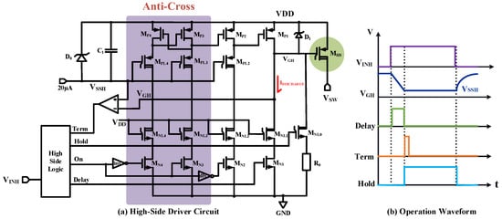
Figure 11.
Proposed high-side driver.
When VINH is low, the built-in level-shifter circuit converts the output signal of the low-voltage domain to the high-voltage domain (VDD~VDD-5V) range; furthermore, the pull-up switch MP1 can turn off the power transistor MHS. In the high-side level-shifter, the two branches of MN3 and MN4 trigger the high-side latch unit with short pulses to quickly lock the high-side output state. As the output stage, the MN2 branch aims to improve the driving capability of the level shifter. The gate drive signal of MN2 should be set with delay time to prevent MP1 and MN1 from conduction simultaneously, so that it can avoid generating a penetrating current flowing from power supply VDD to ground.
When VINH is high, large-sized MN1 pulls down the gate voltage to open MHS quickly. As the gate drain current flows into the reference ground, spike voltage perturbation on the floating rail VDDL will be eliminated. When the gate voltage of MHS is lower than VDDL, the built-in high-voltage comparator immediately outputs a short-pulse Term signal to turn off MN1; in this way, the gate voltage is well-protected. At the same time, the Hold signal is switched to high to open the gate voltage holding branch at MNL0 to maintain the gate voltage of MHS by using the reverse breakdown characteristic of the voltage regulator D1.
2.4. CMTI
CMOS CMTI refers to the irreversible effects of a transient signal in the reference ground on either side of the input or output side, that will be coupled as a common-mode transient pulse into the other side through the isolation capacitor [21]. CMT events with different rates of change produce common-mode transient pulses of different magnitudes. A common-mode event in TX will have two effects on the RX. Firstly, it will generate a large common-mode to differential-mode signal. Secondly, it will result in an offset of the DC operating point at the RX input; a big offset results in erroneous data transmission, such as outputting a high level when the transmitted data should be low.
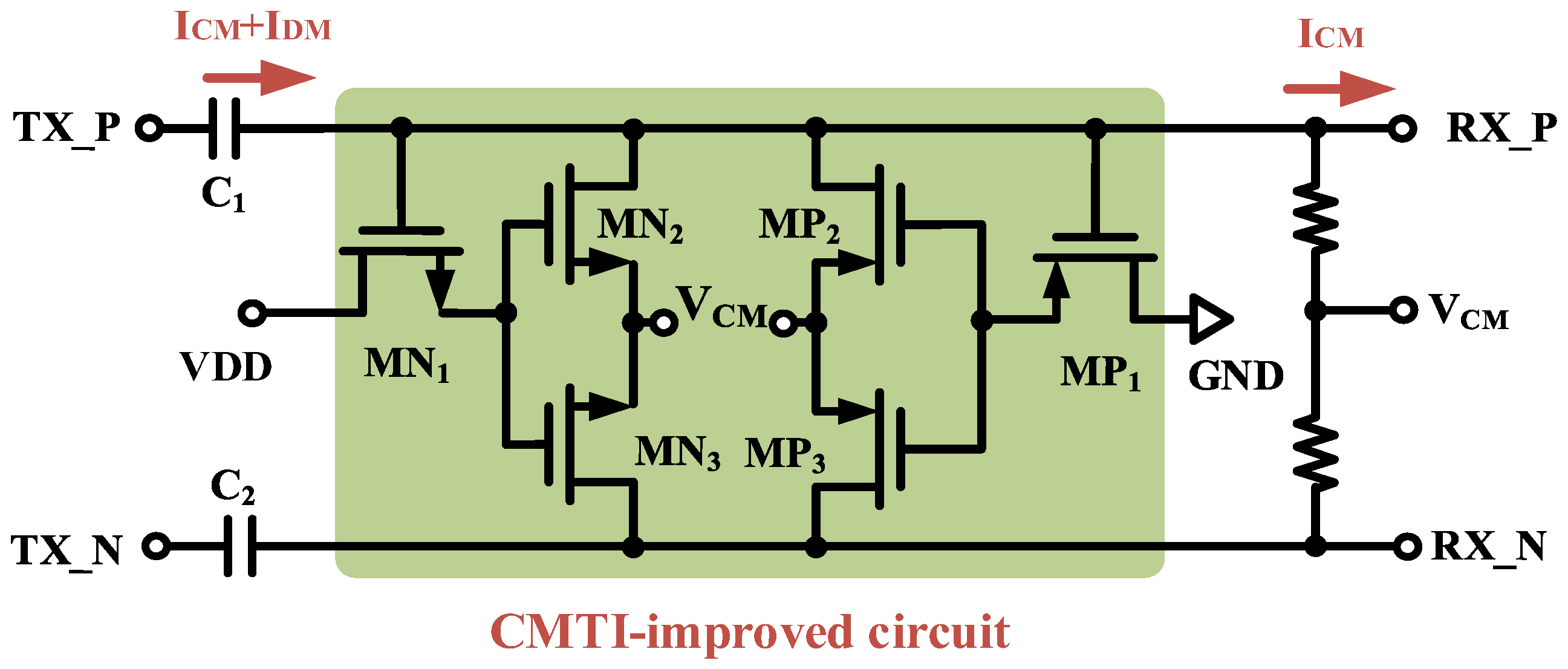
To avoid this situation, a novel active common-mode filtering circuit is proposed, as shown in Figure 12. A small MOS device is utilized to reduce the offset of the DC operating point at the receiver side when a high-speed CMT event occurs. When no CMT event occurs, only the differential-mode small-signal current is output on the isolation capacitor, both MN1 and MP1 are in the offset, and the active common-mode filter circuit does not work. When a positive CMT event occurs, the transient pulse signal will cause the isolation capacitor to output a large positive transient signal; at this time, MN1 was opened, and the isolation capacitor output differential-mode current into the reference ground. Similarly, in case of a negative CMT event, it will cause the isolation capacitor to output a large negative transient signal to make MP1 open, and the compensation current is poured into the receiver from the power supply to maintain the stability of the common-mode potential at the receiver. Additionally, the DC operating point due to common-mode transients can be further reduced by decreasing the size of transistors MN1 and MP1 to lower their threshold voltages.
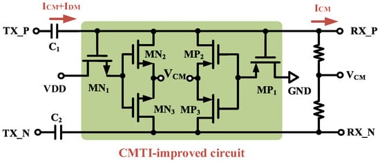
Figure 12.
Active common-mode filter circuit.
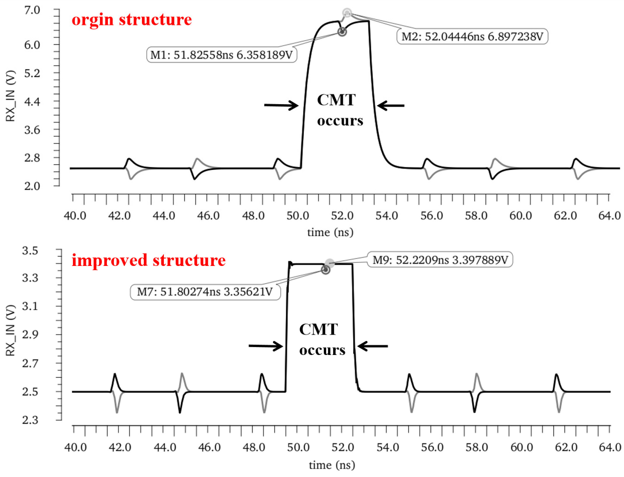
The transient simulation results of the critical node are shown in Figure 13. When a CMT event of 150 kV/μs occurs on the TX side, gate breakdown will occur in the input device at the receiver side of the isolator where clamping is not added. Instead, the inclusion of an active common-mode filter circuit transmits the full differential signal by filtering the common-mode current. And it also avoids transmission errors due to DC operating point offset by reducing the transient voltage drop falling on the common-mode resistor.
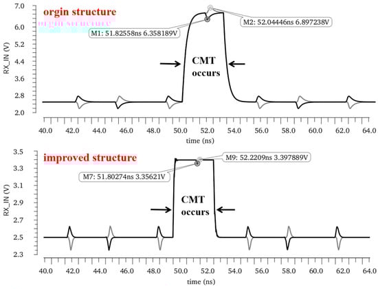
Figure 13.
Diagram of waveform comparison with/without common-mode filter circuit.
3. Post-Simulation Results
Figure 14 shows the overall layout of a dual-channel isolated driver. Based on the X-Fab 0.18 μm CMOS process, the overall layout size is 2092 × 2898 μm2. Every individual transmission channel consists of a TX, RX, and Driver. From the layout, it can be observed that the dual-channel layout is highly symmetric, which is favorable for improving the CMTI of the digital isolator. To make the post-simulation process closer to reality, some parasitic parameters in the isolation part that are easy to ignore are, additionally, considered. Firstly, parasitic inductance and resistance are added to the wires connecting the single channels between the back-to-back capacitors to simulate the actual bonding wires. The effect of the larger parasitic capacitance between the pole plate and the substrate under the isolation capacitor is also considered. In this way, the error between the post-simulation results and the experimental results is minimized.
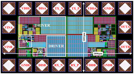
Figure 14.
Layout of dual-channel capacitive digital isolation driver.
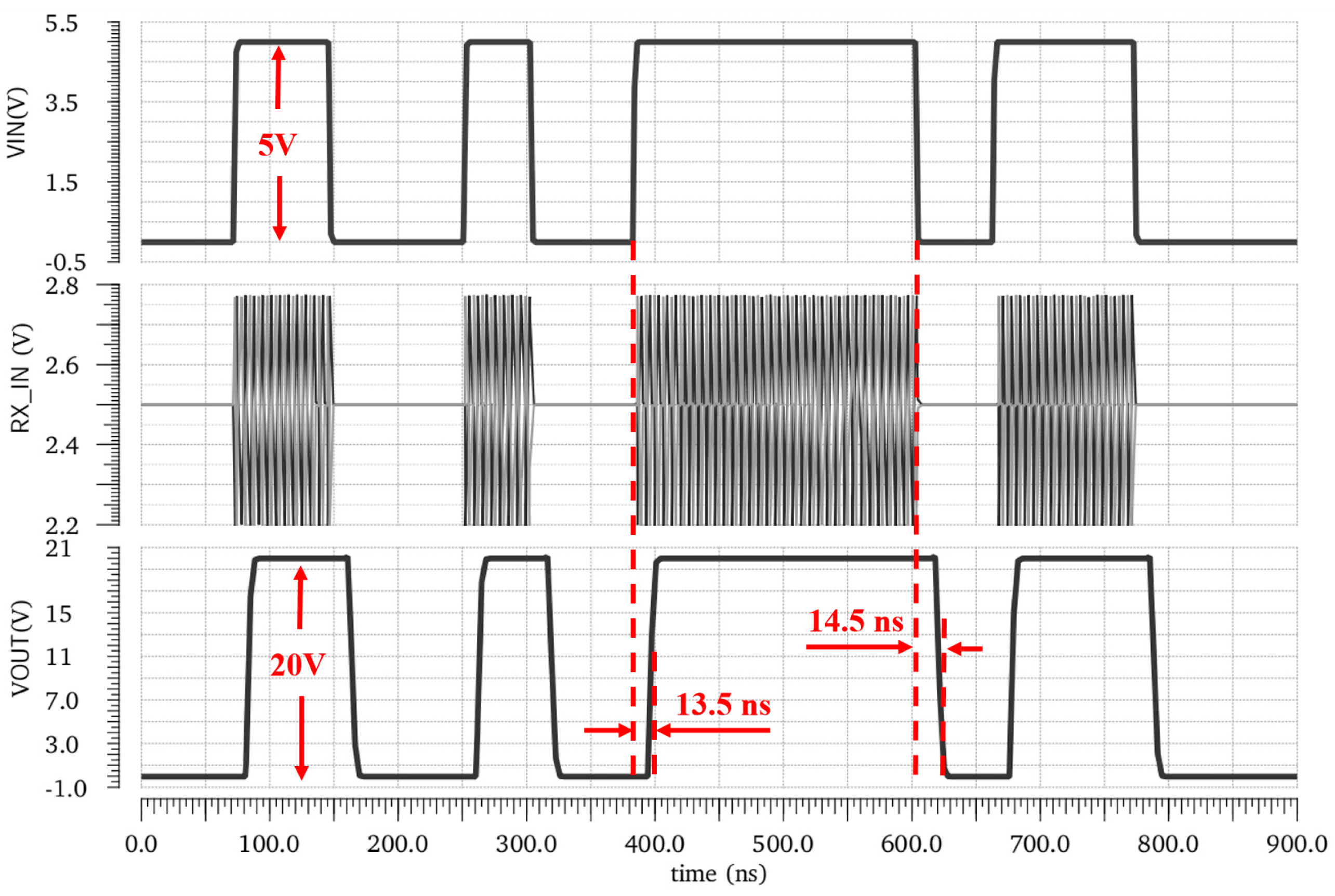
Figure 15 shows the simulated waveforms of the key nodes of the TX, RX, and Driver modules. The input is a five-bit pseudo-random bit sequence (PRBS) mode signal. The typical propagation delay from the input pin to the output pin is 15 ns at the TT process, at 27 °C, with a 1.2 nF load. The post-simulation results illustrate that the designed isolated driver achieves an accurate modulation–demodulation function and an efficient driving function at different data rates. The propagation delay is insensitive to changes in temperature and transmission rate as illustrated in Figure 16.
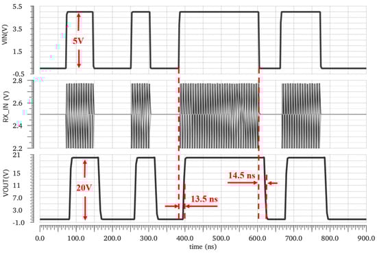
Figure 15.
Simulated waveforms of isolator driver with 1.2 nF load.
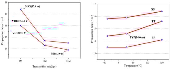
Figure 16.
Propagation delay vs. supply voltage and temperature.
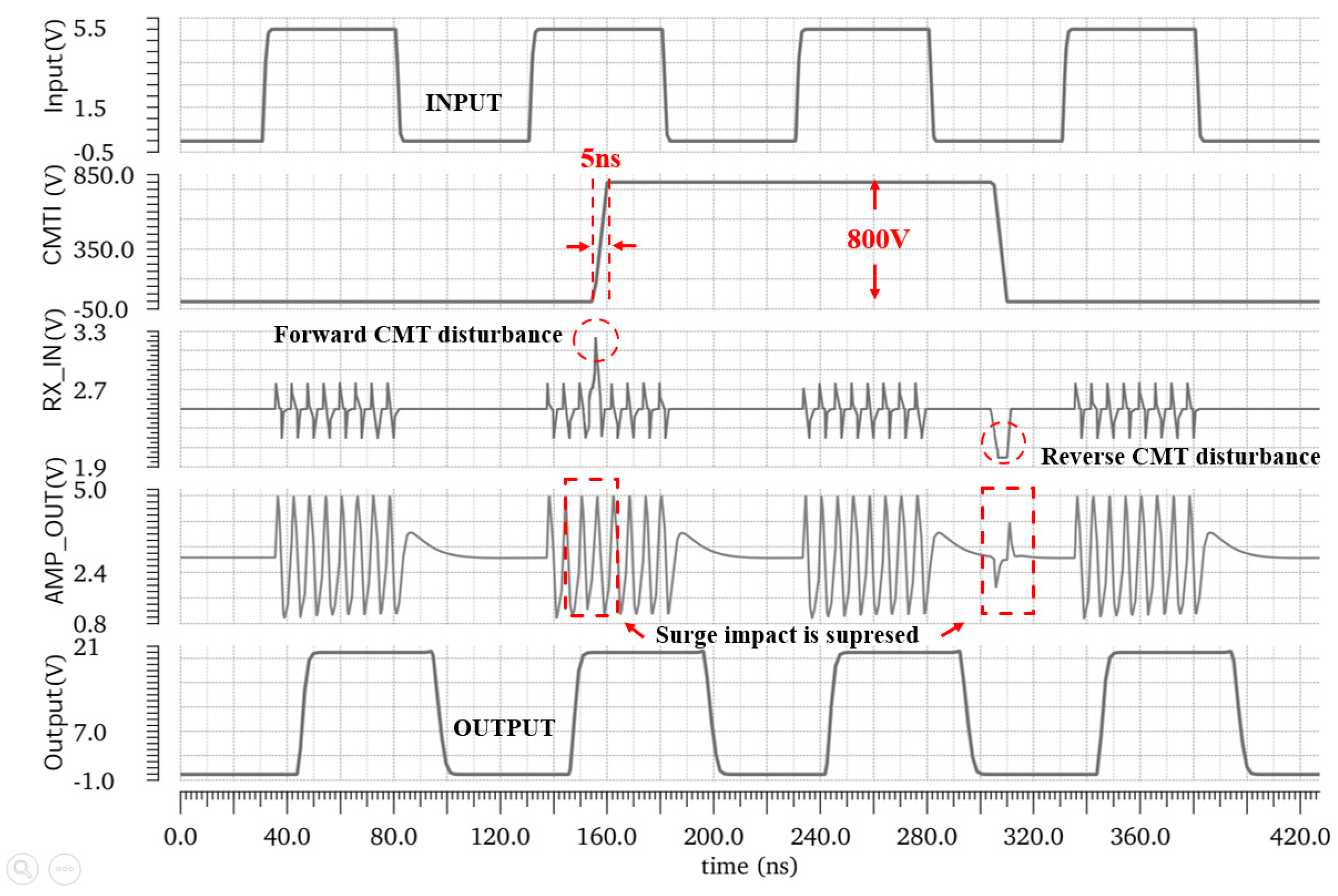
Figure 17 shows the CMTI performance of the digital isolator. A high-voltage signal with an edge rate of 150 kV/μs is added between TX and RX to simulate CMT events. When a 10 MHz, 50% duty cycle square wave signal is input, the back results show that the output has no transmission error. Table 1 compares the simulation results of this design with other previous work. The drive capability of this work is 80 times that of [22], 50 times that of [13], and 25 times that of [12], respectively. The proposed isolated driver achieves a high CMTI capability and low propagation delay.
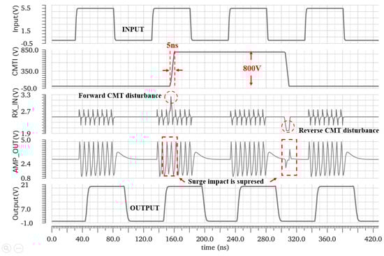
Figure 17.
CMTI events.

Table 1.
Chip specifications.
4. Conclusions
This paper proposes a dual-channel configurable capacitor digital isolation driver in the 0.18 μm CMOS process. A high data transmission rate and low propagation delay are achieved by using the OOK modulation technique and a fully differential transmission form. The fully integrated high-voltage level-shift driver without an off-chip capacitor has a strong driving capability for power devices. An active common-mode filter circuit is proposed to further improve the CMTI capability of the chip, which ultimately achieves a CMTI of higher than 150 kV/μs. The typical propagation delay is less than 15 ns at a 25 Mbps transmission rate with a 1.2 nF load. It can be configured as two signal-side drivers or a DT-programmable half-bridge driver. The isolated drivers can meet the high efficiency and reliability requirements of a wide variety of power supply applications.
Author Contributions
Conceptualization, Y.Z. and L.W.; software simulation and parameter optimization, Y.Z. and C.C.; data processing, Y.Z.; writing—original draft preparation, C.C. and Y.Z.; writing—review and editing, Z.C. and Y.Z.; formal analysis, C.C. and Z.C.; supervision, R.Z. and B.L. All authors have read and agreed to the published version of the manuscript.
Funding
This research was funded by the Natural Science Foundation of Fujian Province (No. 2023H0052) and Major Science and Technology Projects of Xiamen (No. 3502Z20221022).
Data Availability Statement
All the data are reported/cited in the paper.
Conflicts of Interest
The authors declare no conflict of interest. Boyang Li and Ronghua Zheng are employees of Xiamen NewSound Technology Co., Ltd. The paper reflects the views of the scientists, and not the company.
References
- Huang, C.-Y.; Shen, W.C.; Tseng, Y.-H.; King, Y.-C.; Lin, C.-J. A contact-resistive random-access-memory-based true random number generator. IEEE Electron Device Lett. 2012, 33, 1108–1110. [Google Scholar] [CrossRef]
- Balatti, S.; Ambrogio, S.; Wang, Z.; Ielmini, D. True random number generation by variability of resistive switching in oxide-based devices. IEEE J. Emerg. Sel. Top. Circuits Syst. 2015, 5, 214–221. [Google Scholar] [CrossRef]
- Altoobaji, I.; Hassan, A.; Ali, M.; Audet, Y.; Lakhssassi, A. A Low-Power 0.68-Gbps Data Communication System for Capacitive Digital Isolator With 1.9-ns Propagation Delay. IEEE Trans. Very Large Scale Integr. (VLSI) Syst. 2023, 32, 952–956. [Google Scholar] [CrossRef]
- Inohara, M.; Sugahara, S. Basic Characteristics of Thin-Film Single-Layer Coreless Micro-Transformers for Digital Isolators. In Proceedings of the 2022 International Power Electronics Conference (IPEC-Himeji 2022-ECCE Asia), Himeji, Japan, 15–19 May 2022; pp. 2567–2572. [Google Scholar]
- Sadrimanesh, H.; Blaquière, Y.; Nabki, F. Toward 2.5 D structures for multi-channel MEMS acoustic-based digital isolators using through silicon openings. In Proceedings of the 2023 21st IEEE Interregional NEWCAS Conference (NEWCAS), Edinburgh, UK, 26–28 June 2023; pp. 1–5. [Google Scholar]
- Altoobaji, I.; Ali, M.; Hassan, A.; Audet, Y.; Lakhssassi, A. A high speed fully integrated capacitive digital isolation system in 0.35 µm CMOS for industrial sensor interfaces. In Proceedings of the 2021 19th IEEE International New Circuits and Systems Conference (NEWCAS), Toulon, France, 13–16 June 2021; pp. 1–4. [Google Scholar]
- Ke, J.; Feng, J.; Liu, C.; Guan, Z.; Xu, H.; Zhao, M. Digital Isolator Based on On-Chip Transformer for High-Voltage SiC MOSFET. In Proceedings of the 2023 IEEE 7th Conference on Energy Internet and Energy System Integration (EI2), Hangzhou, China, 15–18 December 2023. [Google Scholar]
- Motto, E.; Donlon, J.; Watabe, K.; Kazunari, H.; Araki, T. A Monolithic 500V, 1A Three Phase Motor Driver with Small Line Surface Mount Package. In Proceedings of the 2007 IEEE Industry Applications Annual Meeting, New Orleans, LA, USA, 23–27 September 2007; pp. 1047–1051. [Google Scholar]
- Kaeriyama, S.; Uchida, S.; Furumiya, M.; Okada, M.; Maeda, T.; Mizuno, M. A 2.5 kV isolation 35 kV/us CMR 250 Mbps digital isolator in standard CMOS with a small transformer driving technique. IEEE J. Solid-State Circuits 2011, 47, 435–443. [Google Scholar] [CrossRef]
- Qu, Y.D.C.L.L.S.X.Y.W. A Fully integrated, Low-Cost, High Channel Utilization Digital Isolator in Standard CMOS with 50Mbps and 100kV/μs CMTI. In Proceedings of the Asia Conference on Power and Electrical Engineering, Shanghai, China, 11–13 April 2024. [Google Scholar]
- Nguyen, V.H.; Ly, N.; Alameh, A.H.; Blaquière, Y.; Cowan, G. A versatile 200-V capacitor-coupled level shifter for fully floating multi-MHz gate drivers. IEEE Trans. Circuits Syst. II Express Briefs 2021, 68, 1625–1629. [Google Scholar] [CrossRef]
- Instruments, T. ISO7041 Ultra-Low Power Four-Channel Digital Isolator. Available online: https://www.ti.com/lit/ds/symlink/iso7041.pdf?ts=1716176779603 (accessed on 1 March 2020).
- MAXIM. MAX14850. Available online: https://www.analog.com/media/en/technical-documentation/data-sheets/MAX14850.pdf (accessed on 9 September 2019).
- Xiong, Z.; Pan, D.; Li, G.; Cheng, L. A 250Mbps 100kV/µs CMTI On-Chip Double-Isolated Transformer-Based Digital Isolator. In Proceedings of the 2022 IEEE International Conference on Integrated Circuits, Technologies and Applications (ICTA), Xi’an, China, 28–30 October 2022; pp. 156–157. [Google Scholar]
- Luo, Y.; Fang, J.; Zhang, E.; Li, M.; Zhang, B. A Novel Cross-Over CMR Transformer Technology for Magnetic Isolation Gate Driver Applications. In Proceedings of the 2019 31st International Symposium on Power Semiconductor Devices and ICs (ISPSD), Shanghai, China, 15–23 May 2019; pp. 123–126. [Google Scholar]
- Ke, X.; Ma, D.B. A 3-to-40V V IN 10-to-50MHz 12W isolated GaN driver with self-excited t dead minimizer achieving 0.2 ns/0.3 ns t dead, 7.9% minimum duty ratio and 50V/ns CMTI. In Proceedings of the 2018 IEEE International Solid-State Circuits Conference-(ISSCC), San Francisco, CA, USA, 11–15 February 2018; pp. 386–388. [Google Scholar]
- Landau, H. Sampling, data transmission, and the Nyquist rate. Proc. IEEE 1967, 55, 1701–1706. [Google Scholar] [CrossRef]
- Kelam, M.; Battu, B.Y.; Abbas, Z. A Compact, Power Efficient, Self-Adaptive and PVT Invariant CMOS Relaxation Oscillator. In Proceedings of the 2020 IEEE Computer Society Annual Symposium on VLSI (ISVLSI), Limassol, Cyprus, 6–8 July 2020; pp. 1–6. [Google Scholar]
- Zangpo, J.; Póvoa, R.; Guilherme, J.; Horta, N. An Integrated LC Oscillator with Self Compensation for Frequency Drift and PVT Corners Variations. In Proceedings of the 2018 25th IEEE International Conference on Electronics, Circuits and Systems (ICECS), Bordeaux, France, 9–12 December 2018; pp. 333–336. [Google Scholar]
- Chen, G.; Jin, Z.; Deng, Y.; He, X.; Qing, X. Principle and topology synthesis of integrated single-input dual-output and dual-input single-output DC–DC converters. IEEE Trans. Ind. Electron. 2017, 65, 3815–3825. [Google Scholar] [CrossRef]
- Xie, H.; Wang, Z.; Liu, G.; Lu, J.; Yi, X. A novel active—Input cascode current mirror with high precision and low power dissipation. Eng. Rep. 2022, 4, e12451. [Google Scholar] [CrossRef]
- Ke, X.; Chen, M. High Common-Mode Transient Immunity High Voltage Level Shifter; Thompson, Andrew John Withers & Rogers LLP: London, UK, 2020. [Google Scholar]
- Devices, A. iCoupler Digital Isolator ADuM1100. Available online: https://www.analog.com/media/en/technical-documentation/data-sheets/ADUM1100.pdf (accessed on 15 July 2015).
- Infineon. 1EDI EiceDRIVER. Available online: https://www.infineon.com/dgdl/Infineon-1EDIXXI12AF-DataSheet-v01_10-EN.pdf?fileId=db3a3043427ac3e201428e648a333734 (accessed on 10 November 2014).


Disclaimer/Publisher’s Note: The statements, opinions and data contained in all publications are solely those of the individual author(s) and contributor(s) and not of MDPI and/or the editor(s). MDPI and/or the editor(s) disclaim responsibility for any injury to people or property resulting from any ideas, methods, instructions or products referred to in the content. |
© 2024 by the authors. Licensee MDPI, Basel, Switzerland. This article is an open access article distributed under the terms and conditions of the Creative Commons Attribution (CC BY) license (https://creativecommons.org/licenses/by/4.0/).