Article

Positive Bias Temperature Instability in SiC-Based Power MOSFETs

1
Advanced Research Center on Electronic System, Department of Electrical, Electronic and Information Engineering, University of Bologna, 47522 Cesena, Italy
2
STMicroelectronics, SRL, Stradale Primosole 50, 95121 Catania, Italy
*
Authors to whom correspondence should be addressed.
Micromachines 2024, 15(7), 872; https://doi.org/10.3390/mi15070872
Submission received: 7 June 2024 / Revised: 25 June 2024 / Accepted: 28 June 2024 / Published: 30 June 2024
(This article belongs to the Special Issue Research Progress of Advanced SiC Semiconductors)

Abstract

:
This paper investigates the threshold voltage shift (ΔVTH) induced by positive bias temperature instability (PBTI) in silicon carbide (SiC) power MOSFETs. By analyzing ΔVTH under various gate stress voltages (VGstress) at 150 °C, distinct mechanisms are revealed: (i) trapping in the interface and/or border pre-existing defects and (ii) the creation of oxide defects and/or trapping in spatially deeper oxide states with an activation energy of ~80 meV. Notably, the adoption of different characterization methods highlights the distinct roles of these mechanisms. Moreover, the study demonstrates consistent behavior in permanent ΔVTH degradation across VGstress levels using a power law model. Overall, these findings deepen the understanding of PBTI in SiC MOSFETs, providing insights for reliability optimization.

1. Introduction

The rapid growth of renewable energy [1] and electric vehicles (EVs) [2] is driving the development of power devices based on wide bandgap (WBG) semiconductors. Renewable energy sources such as solar and wind energy require efficient solutions to convert and manage electricity [3], as well as electric vehicles requiring high-power reliable semiconductor devices to control electric motors and charging systems [4].
Silicon carbide (SiC) stands out in the realm of power electronics, offering a robust and high-performance alternative to conventional silicon (Si) counterparts [5], thus representing one of the best choices for applications where high power and reliability are required, such as solar inverters, wind turbine control systems, and electric vehicle motor control systems.
SiC’s inherent properties enable devices to operate at higher voltages, maintain stability at elevated temperatures, and switch at high frequencies. In particular, the breakdown electric field strength, nearly ten-fold that of silicon, and a band gap three times wider [6], allow for operation at elevated voltages and temperatures. Another key advantage of SiC lies in its thermal performance; it can maintain consistent operation even under high-temperature conditions [7], which is crucial for many industrial and automotive applications. The high thermal conductivity of SiC also aids in mitigating temperature-dependent degradation, ensuring longevity and reliability.
The high-frequency operation capability of SiC devices enables more compact power electronics systems [8], offering higher power density and reduced cooling requirements and opening a spectrum of possibilities in various sectors, from power systems to switch-mode power supplies and EVs [9].
However, while SiC technology offers significant benefits, different challenges are still present, including intricate production processes, resulting in elevated costs, and notably, issues related to device reliability.
One reliability challenge is the lower short circuit tolerance of SiC devices compared with Si ones [10,11]. This necessitates the use of fast-acting gate drivers to ensure device safety and reliability. In addition, SiC devices have been observed to exhibit larger threshold voltage (VTH) instability compared with their Si counterparts, with a tendency to faster recovery [12,13,14]. In [15], two distinct trapping mechanisms contributing to VTH shift (ΔVTH) have been identified under gate bias stress tests, i.e., trapping of charges in the near-interface oxide traps (also referred as border traps) and in intrinsic defects at the SiO2/SiC interface.
The presence of pre-existing border traps has also been investigated in [16,17,18,19,20], highlighting the role of the tunneling in the charging and discharging processes [19], and measuring capture and emission times in the order of μs [20]. The role of fast trapping mechanisms related to pre-existing interface defects has been analyzed in [21,22,23,24].
In addition to interface and border defects, the creation of new traps and/or the charge trapping in deeper energy-level defects, both localized within the oxide, has been demonstrated in [25] by applying a relatively large gate voltage.
Further investigations have indicated the role of the testing methods on the observed ΔVTH. In particular, the influence of positive/negative bias temperature instability (P/NBTI) on the electrical characteristics of SiC MOSFETs has been thoroughly studied using both slow and fast measurement techniques [26].
Recently, we reported a distinct temperature dependence of ΔVTH, which varies based on the measurement technique employed [27]. When using a slow-PBTI procedure, the effect of fast interface and border traps is not accounted for in ∆VTH, as their recovery time is shorter than the VTH characterization time. As a result, the oxide charge trapping dominates ΔVTH, resulting in a positive temperature dependency, i.e., the higher the temperature, the greater the charge trapping, the higher ∆VTH. Conversely, a negative temperature dependency is observed when a fast-PBTI test is adopted, emphasizing the role of a fast interface and border traps in the overall behavior [27].
In this work, the ∆VTH of SiC MOSFETs induced by different PBTI test procedures suggested by JEDEC JEP184 [28], here named transistor and diode modes, has been investigated. The role of the gate bias level on the different underneath trapping mechanisms has been analyzed.

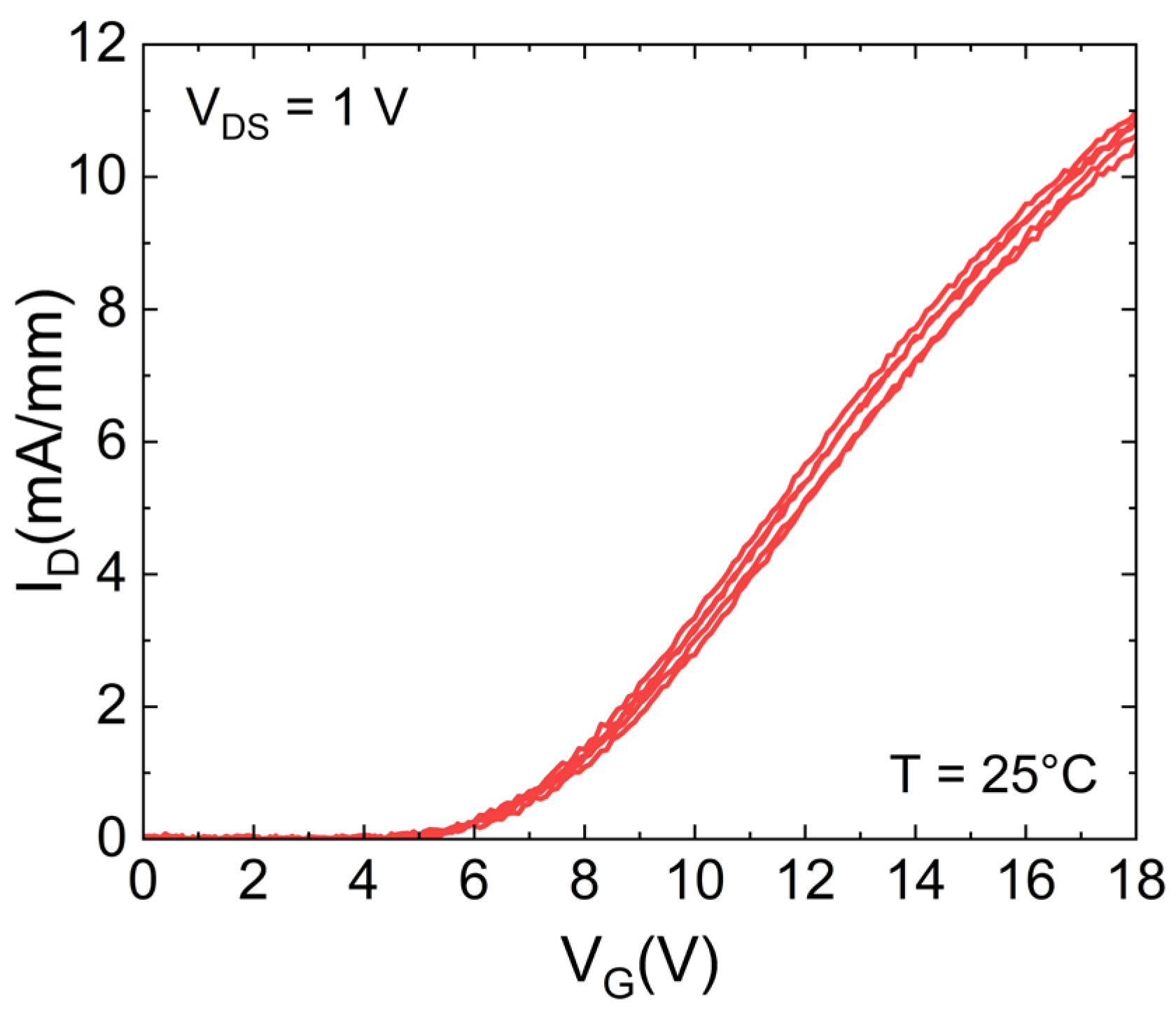
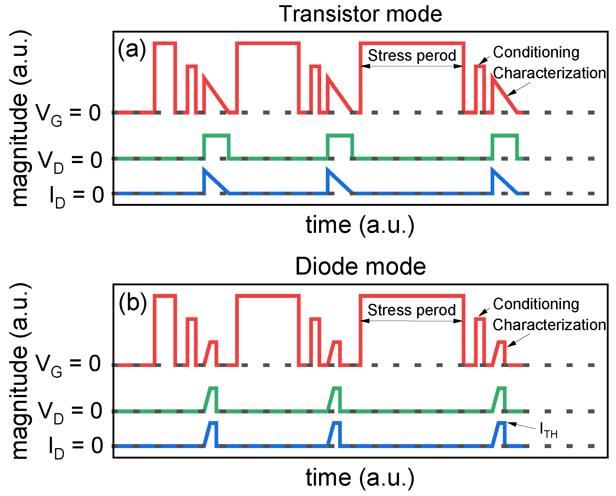
2. Devices under Test (DUTs) and BTI Characterization Techniques

In this study, a 650 V automotive grade silicon carbide power MOSFET with a vertical-diffused structure (VD-MOSFET), manufactured by STMicroelectronics, has been considered. The room temperature transfer characteristics is reported in Figure 1, additional key features can be found in [29].
The Keysight Power Device Analyzer B1505A has been adopted for this analysis.
Initially, a PBTI stress and characterization procedure according to the JEDEC standard JEP184, namely transistor mode, has been adopted and reported in Figure 2a. It illustrates the gate voltage (VG), drain voltage (VD), and drain current (ID) for the initial three stress and characterization periods. The gate maintains a steady bias during the stress phase, while the drain and source are grounded. Stress time periods, which increase logarithmically, are interspersed with VTH sensing intervals. Following each stress interval, the gate stress is removed to allow for conditioning and VTH sensing. To stabilize the VTH readout, a conditioning phase is carried out by a 100 ms long positive gate pulse before the VTH measurement. For the extrapolation of VTH, the ID–VG transfer characteristics are measured. During this process, VD remains constant whereas VG is swept from VG_MAX to 0 V to minimize VTH recovery. VTH is calculated at fixed ID = 1 mA.
However, as ΔVTH can be induced by slow and fast trapping/de-trapping components [16,17,18,19,20,21,22,23,24,25], slower measurements might result in the partal loss of the contribution ascribed to faster defects, i.e., fast defects recover before and/or during the VTH characterization phase, thus not contributing to it. To gain a clearer understanding of these fast components, it is necessary to use faster measurement techniques.
Standard JEP184 also provides the gated-diode method for measuring the VTH of SiC power transistors under BTI stress conditions. It involves biasing both the VG and VD simultaneously while maintaining the source at the ground potential. The test consists of two blocks: a stress phase for a specified period and VTH characterization.
Similar to the previous method, during stress, VG stress is applied to the gate terminal. The increasing gate stress time corresponds to a logarithmic scale.
The VTH measurement method follows the JEDEC standard JEP183 [30], shown in Figure 2b. Firstly, as for the previous method, a gate conditioning pulse is applied, then VTH of the SiC power MOSFET is measured in diode mode, which consists of the shorting gate and drain. The instrument forces the target threshold current (ITH), which determines the VTH with a faster spot measurement (10 ms) compared with the full IDVG characterization (few seconds), therefore avoiding VTH recovery as much as possible.

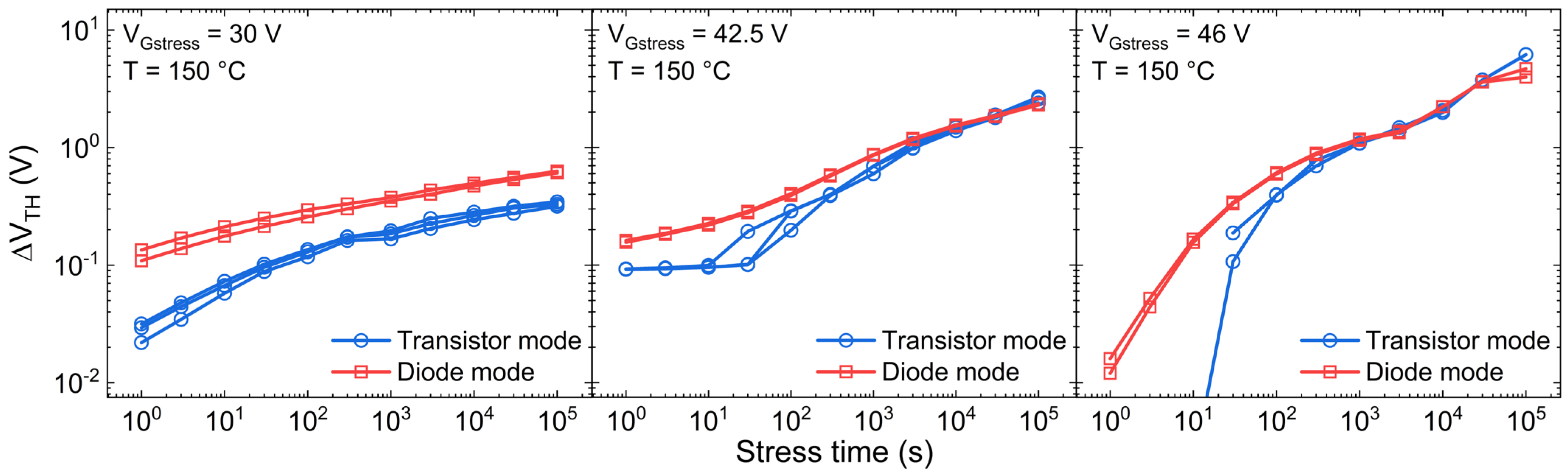
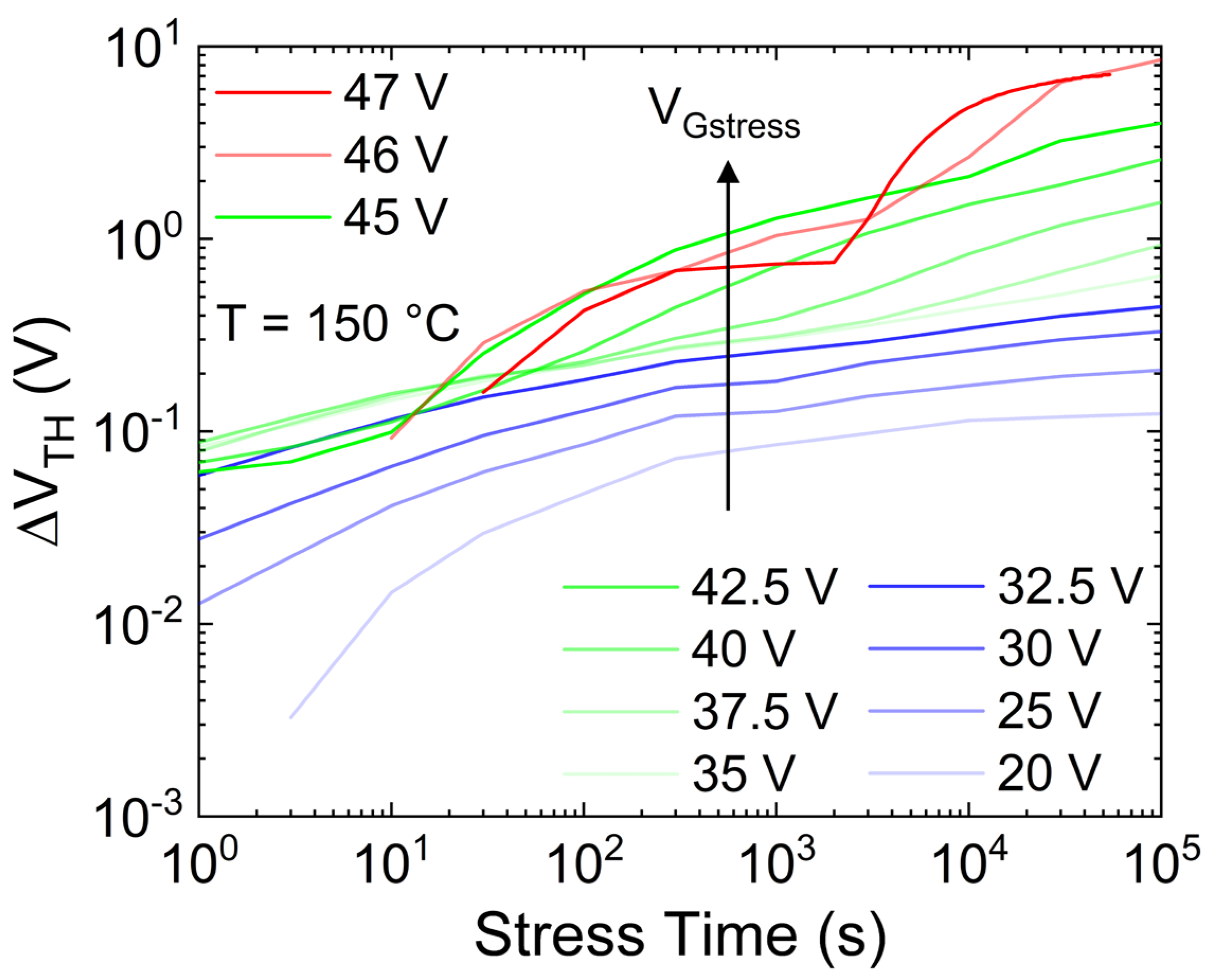
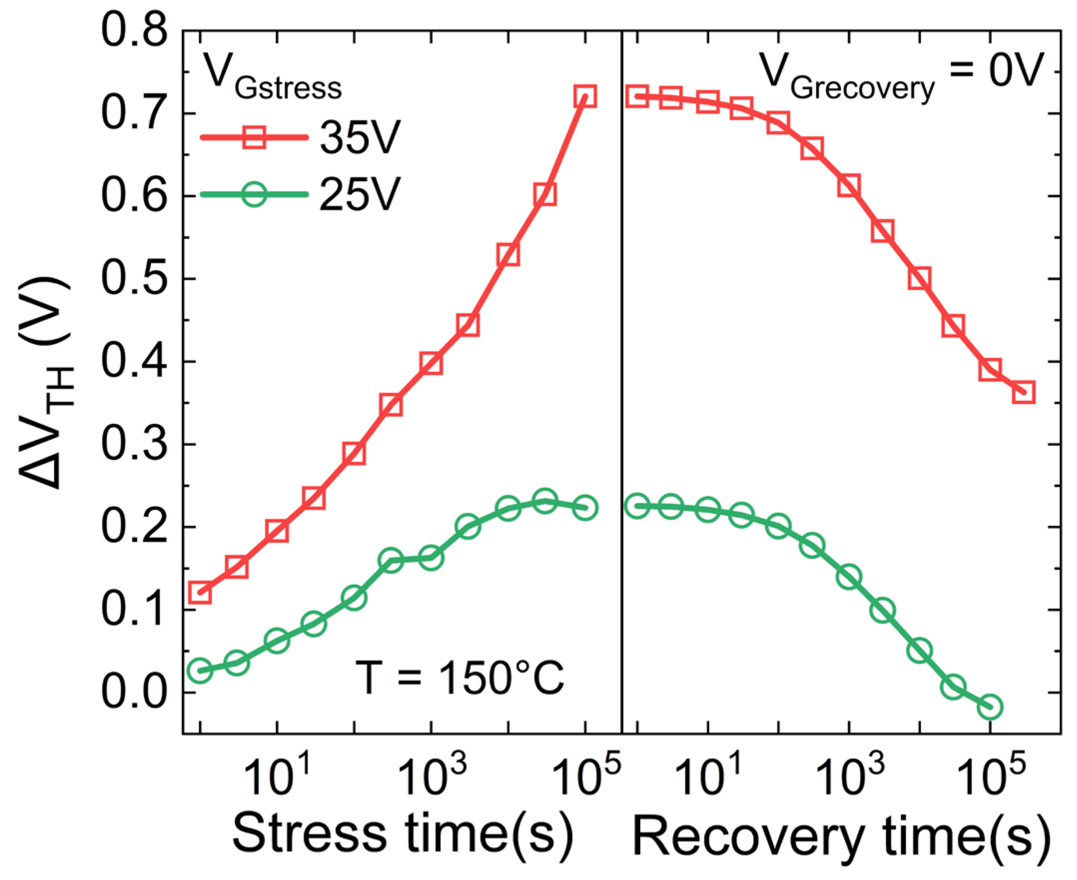
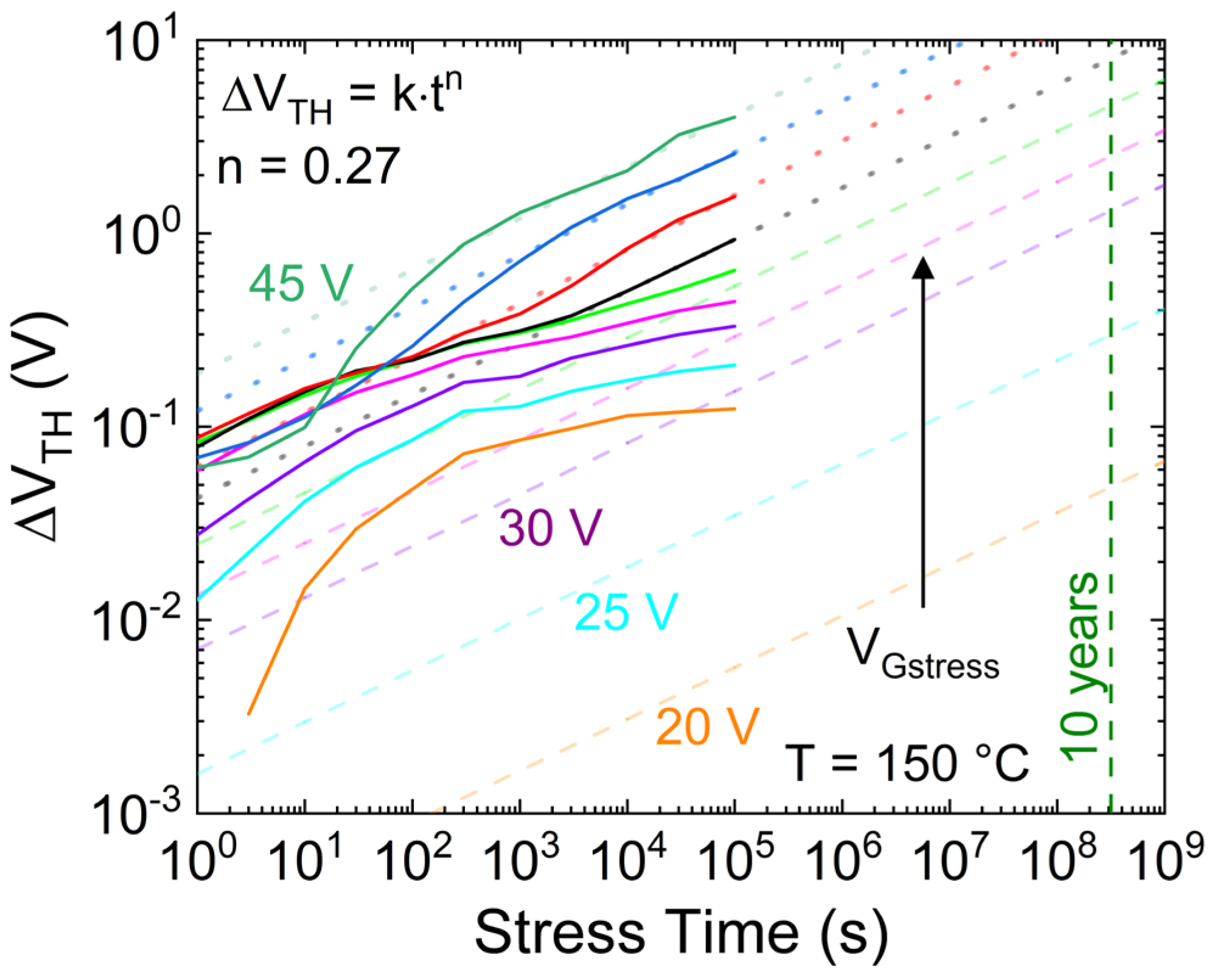
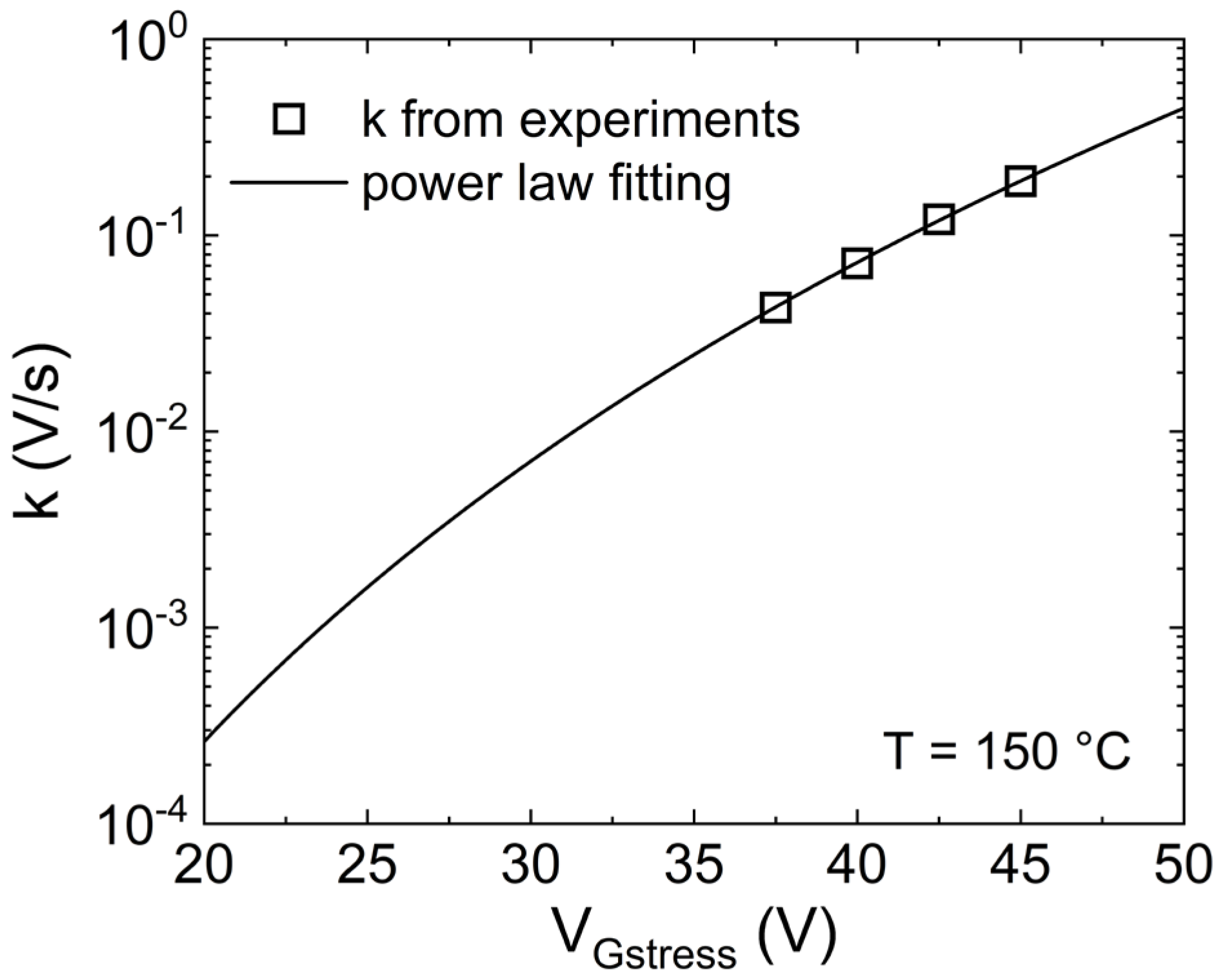
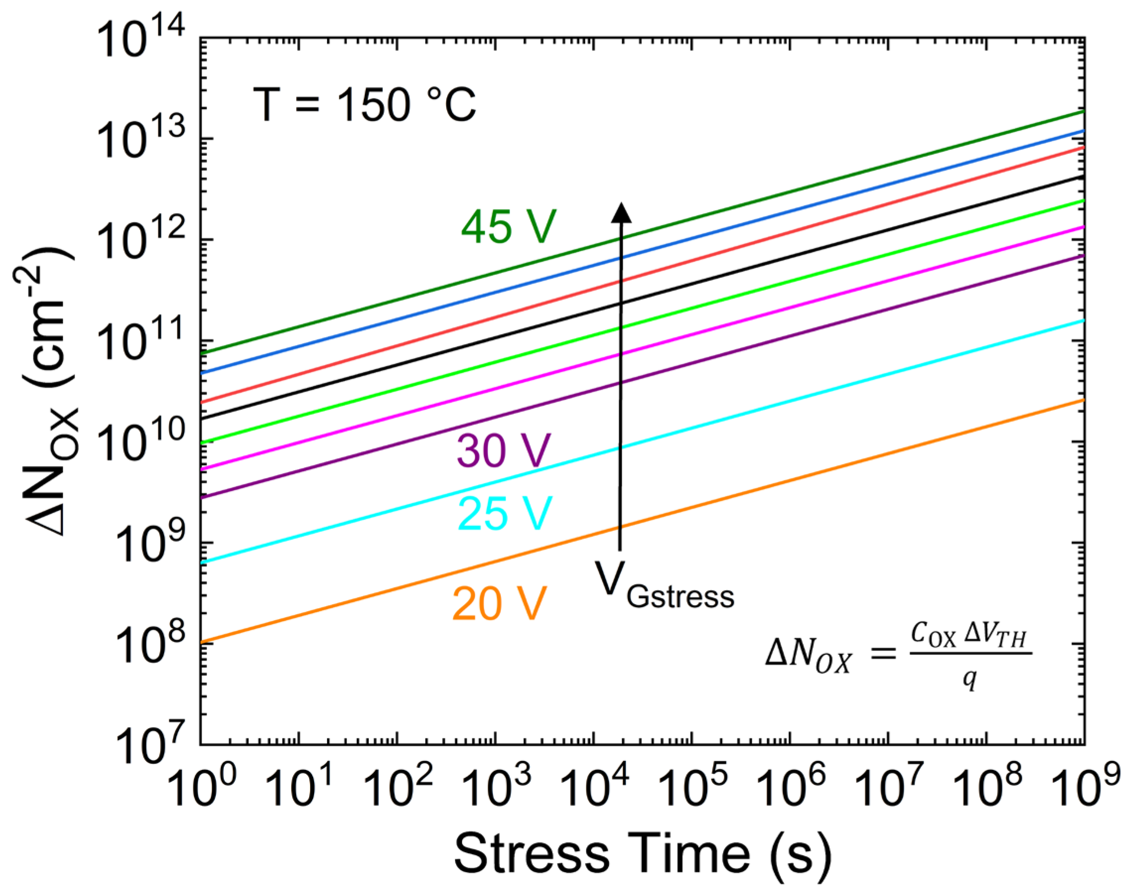
3. Results and Discussion

Figure 3 reports the ΔVTH under different gate stress voltages (VGstress) at an ambient temperature of 150 °C. Notably, the ΔVTH obtained by means of the diode mode approach is higher, especially for lower VGstress values (i.e., 30 V), although the stress phase is the same. The difference is ascribed to the different characterization phase, which is temporally shorter in the case of diode mode, allowing for a smaller VTH recovery, hence capturing a larger ∆VTH. The difference between the two methods becomes more pronounced when operating at lower VGstress settings or for shorter stress durations. This is because the trapping and de-trapping processes in/from shallow pre-existing defects, which demand less time to capture and release charges, emerge as the predominant mechanism responsible for ΔVTH. As the gate voltage and stress time increase, the creation of new defects or the trapping in spatially deeper oxide defects starts to play a significant role, producing a permanent or slowly recoverable ∆VTH. As a result, the different characterization time that distinguishes the two methods no longer has an impact on the ∆VTH, as the recoverable part is negligible with respect to the permanent one.
To demonstrate the occurrence of an additional mechanism (creation of new oxide defects or trapping in spatially deeper defects) with respect to trapping in the pre-existing defects, the PBTI analysis is performed at different VGstress ranging from 20 V to 47 V; the latter is a few volts below the breakdown voltage. Figure 4 shows ΔVTH versus the stress time as a function of different applied VGstress. It is possible to note the following: (i) for VGstress up to 32.5 V, the long-term ∆VTH shows signs of saturation. This confirms the trapping in pre-existing defects with a finite concentration; (ii) from VGstress = 35 V to VGstress = 45 V, the ∆VTH shows a second (higher) slope, indicating the triggering of an additional trapping mechanism, which occurs at shorter stress times by increasing VGstress; (iii) for VGstress > 45 V, i.e., close to breakdown voltage, further trapping mechanisms seem to show up producing a further ∆VTH slope variation. Moreover, under these high field conditions, a negative or smaller threshold voltage drift is observed for short stress times (<30 s), while a negligible VGstress dependency is observed for long stress times (>104 s), indicating the presence of an additional competing mechanism, e.g., electron de-trapping from the oxide to the gate metal, contributing to VTH decrease. Overall, by focusing on the long-term behavior reported in points (ii) and (iii), it may be ascribed to the creation of new oxide defects or charge trapping into spatially deep states, i.e., oxide traps far away from the SiO2/SiC interface.
To strengthening this hypothesis, a stress test followed by the recovery phase has been carried out in the case of VGstress = 25 V and 35 V. Figure 5 reports a permanent or slowly recoverable ∆VTH, even after an extended recovery period of approximately 83 h at 150 °C, in the case of VGstress = 35 V, i.e., the bias condition in which ∆VTH shows the occurring of a second slope. On the contrary, a lower stress level of VGstress = 25 V leads to a full recoverable ΔVTH within just a few hours, confirming trapping and de-trapping in shallow pre-existing defects.
Focusing on the dynamics of ΔVTH leading to permanent degradation (VGstress ≥ 35 V), it can model by using a power law, as shown in Figure 6. It is worth noting that ΔVTH curves with VGstress > 45 V have not been considered because they are very close to the breakdown voltage. Therefore, the additional observed mechanisms are unlikely to occur under normal operating conditions. Figure 6 illustrates that the effect of the second mechanism on ΔVTH, whether it is creating new defects or trapping in spatially deeper states, always shows the same power slope (exponent) of n = 0.27, regardless of the gate stress voltage. Consequently, it is possible to assume that the same mechanism occurs even at lower VGstress, but its impact is masked by trapping in the shallow pre-existing defects during the observed time windows. In particular, by obtaining the scaling factor k (symbols in Figure 7) through fitting the region of ΔVTH experiments with steeper slope (dotted lines in Figure 6), the dependency of k on the gate voltage can be analyzed, resulting in a power-law relationship, as depicted in Figure 7. Consequently, the effect of this second mechanism can be estimated even at gate voltages closer to nominal operation (dashed lines in Figure 6) by deriving k from the model presented in Figure 7, utilizing n = 0.27. For instance, considering a maximum VG = 25 V, the induced ∆VTH due to the creation of new defects is estimated to be roughly 300 mV after 10 years at 150 °C.
By considering the ∆VTH ascribed to the oxide charge trapping (i.e., dotted and dashed lines in Figure 6), the corresponding oxide trapped charge density (∆NOX) is calculated and reported in Figure 8 as a function of VGstress. It is worth noting that the possible creation of new interface and/or border defects is excluded because, as demonstrated in [27], no degradation of the subthreshold slope has been observed (not shown).
Finally, a temperature-dependent PBTI analysis has been carried out to calculate the activation energy of the oxide traps inducing permanent or slowly recoverable ∆VTH, hence degradation. In particular, VGstress = 42.5 V has been adopted as it represents the bias condition in which the second ∆VTH slope (trapping mechanism of interest) is clearly visible, whereas the short-term additional mechanism occurring at larger gate biases (close to the breakdown voltages) is almost negligible. As observed from the Arrhenius plot in Figure 9, such oxide defects feature an activation energy of ~80 meV. The relatively shallow energy level combined with the long recovery time (permanent) further confirms the creation of new oxide defects or the trapping in states far away from the SiC/SiO2 interface (spatially deep).

4. Conclusions

The positive bias temperature instability of SiC MOSFETs has been analyzed, revealing insights into the underlying mechanisms contributing to ΔVTH. The results demonstrate the importance of characterization methods, with the diode mode approach proving more sensitive to fast pre-existing defects compared with the transistor mode one, because of the reduced VTH measure time, eventually leading to a smaller recovery. The analysis of ΔVTH under different gate stress voltage conditions confirmed the presence of multiple trapping mechanisms, including trapping in pre-existing defects and the creation of new defects or trapping in spatially deeper states. These mechanisms exhibit distinct behaviors at varying VGstress levels, contributing to permanent or slowly recoverable ΔVTH. Overall, the findings contribute to a deeper understanding of the PBTI phenomena in SiC MOSFETs and provide valuable insights for enhancing device reliability.

Author Contributions

Conceptualization, S.B., A.-l.R., C.F., E.S. and A.N.T.; Methodology, V.V., S.B., L.A., G.T., E.F., A.-l.R. and A.N.T.; Formal analysis, V.V.; Investigation, V.V.; Data curation, A.N.T.; Writing—original draft, V.V.; Writing—review & editing, S.B., L.A., G.T., E.F., A.-l.R., C.F., E.S. and A.N.T.; Supervision, A.N.T.; Funding acquisition, C.F., E.S. and A.N.T. All authors have read and agreed to the published version of the manuscript.

Funding

This work is partly funded by TRANSFORM, a European co-funded innovation project granted by the ECSEL Joint Undertaking (JU) under grant agreement No. 101007237.

Data Availability Statement

The original contributions presented in the study are included in the article.

Conflicts of Interest

Authors S.B.; L.A.; G.T.; E.F.; A.-l.R. were employed by the company STMicroelectronics. The remaining authors declare that the research was conducted in the absence of any commercial or financial relationships that could be construed as a potential conflict of interest.

References

  1. Mysiński, W. SiC mosfet transistors in power analog application. In Proceedings of the 2017 19th European Conference on Power Electronics and Applications (EPE’17 ECCE Europe), Warsaw, Poland, 11–14 September 2017; pp. P.1–P.7. [Google Scholar] [CrossRef]
  2. Kumar, K.; Bertoluzzo, M.; Buja, G. Impact of SiC MOSFET traction inverters on compact-class electric car range. In Proceedings of the 2014 IEEE International Conference on Power Electronics, Drives and Energy Systems (PEDES), Mumbai, India, 16–19 December 2014; pp. 1–6. [Google Scholar] [CrossRef]
  3. Hatanaka, A.; Kageyama, H.; Masuda, T. A 160-kW high-efficiency photovoltaic inverter with paralleled SiC-MOSFET modules for large-scale solar power. In Proceedings of the 2015 IEEE International Telecommunications Energy Conference (INTELEC), Osaka, Japan, 18–22 October 2015; pp. 1–5. [Google Scholar] [CrossRef]
  4. Marcuzzi, A.; Favero, D.; Santi, C.D.; Meneghesso, G.; Zanoni, E.; Meneghini, M. A Review of SiC Commercial Devices for Automotive: Properties and Challenges. In Proceedings of the 2023 AEIT International Conference on Electrical and Electronic Technologies for Automotive (AEIT AUTOMOTIVE), Modena, Italy, 17–19 July 2023; pp. 1–6. [Google Scholar] [CrossRef]
  5. Alharbi, S.S.; Alharbi, S.S.; Al-bayati, A.M.S.; Matin, M. A comparative performance evaluation of Si IGBT, SiC JFET, and SiC MOSFET power devices for a non-isolated DC-DC boost converter. In Proceedings of the 2017 North American Power Symposium (NAPS), Morgantown, WV, USA, 17–19 September 2017; pp. 1–6. [Google Scholar] [CrossRef]
  6. Liu, T.; Hu, S.; Wang, J.A.; Guo, G.; Luo, J.; Wang, Y.; Guo, J.; Huo, Y. An Investigation of Electric Field and Breakdown Voltage Models for a Deep Trench Superjunction SiC VDMOS. IEEE Access 2019, 7, 145118–145123. [Google Scholar] [CrossRef]
  7. Yu, H.; Jiang, X.; Chen, J.; Shen, Z.J.; Wang, J. Comparative Study of Temperature Sensitive Electrical Parameters for Junction Temperature Monitoring in SiC MOSFET and Si IGBT. In Proceedings of the 2020 IEEE 9th International Power Electronics and Motion Control Conference (IPEMC2020-ECCE Asia), Nanjing, China, 29 November–2 December 2020; pp. 905–909. [Google Scholar] [CrossRef]
  8. Karami, M.; Tallam, R. Thermal Characterization of SiC Modules for Variable Frequency Drives. In Proceedings of the 2019 IEEE Energy Conversion Congress and Exposition (ECCE), Baltimore, MD, USA, 29 September–3 October 2019; pp. 4944–4949. [Google Scholar] [CrossRef]
  9. Biela, J.; Schweizer, M.; Waffler, S.; Kolar, J.W. SiC versus Si—Evaluation of Potentials for Performance Improvement of Inverter and DC–DC Converter Systems by SiC Power Semiconductors. IEEE Trans. Ind. Electron. 2011, 58, 2872–2882. [Google Scholar] [CrossRef]
  10. Bashar, E.; Wu, R.; Agbo, N.; Mendy, S.; Jahdi, S.; Gonzalez, J.O.; Alatise, O. Comparison of Short Circuit Failure Modes in SiC Planar MOSFETs, SiC Trench MOSFETs and SiC Cascode JFETs. In Proceedings of the 2021 IEEE 8th Workshop on Wide Bandgap Power Devices and Applications (WiPDA), Redondo Beach, CA, USA, 7–11 November 2021; pp. 384–388. [Google Scholar] [CrossRef]
  11. Singh, R.; Grummel, B.; Sundaresan, S. Short circuit robustness of 1200 V SiC switches. In Proceedings of the 2015 IEEE 3rd Workshop on Wide Bandgap Power Devices and Applications (WiPDA), Blacksburg, VA, USA, 2–4 November 2015; pp. 1–4. [Google Scholar] [CrossRef]
  12. Puschkarsky, K.; Grasser, T.; Aichinger, T.; Gustin, W.; Reisinger, H. Review on SiC MOSFETs High-Voltage Device Reliability Focusing on Threshold Voltage Instability. IEEE Trans. Electron Devices 2019, 66, 4604–4616. [Google Scholar] [CrossRef]
  13. Ghosh, A.K.; Hao, J.; Cook, M.; Suliman, S.A.; Wang, X.; Awadelkarim, O.O. Threshold-voltage bias-instability in SiC MOSFETs: Effects of stress temperature and level on oxide charge buildup and recovery. Semicond. Sci. Technol. 2022, 37. [Google Scholar] [CrossRef]
  14. Aichinger, T.; Rescher, G.; Pobegen, G. Threshold voltage peculiarities and bias temperature instabilities of SiC MOSFETs. Microelectron. Reliab. 2018, 80, 68–78. [Google Scholar] [CrossRef]
  15. Fiorenza, P.; Giannazzo, F.; Cascino, S.; Saggio, M.; Roccaforte, F. Identification of two trapping mechanisms responsible of the threshold voltage variation in SiO2/4H-SiC MOSFETs. Appl. Phys. Lett. 2020, 117, 103502. [Google Scholar] [CrossRef]
  16. Moghadam, H.A.; Dimitrijev, S.; Han, J.; Haasmann, D.; Aminbeidokhti, A. Transient-Current Method for Measurement of Active Near-Interface Oxide Traps in 4H-SiC MOS Capacitors and MOSFETs. IEEE Trans. Electron Devices 2015, 62, 2670–2674. [Google Scholar] [CrossRef]
  17. Carangelo, G.; Reggiani, S.; Consentino, G.; Crupi, F.; Meneghesso, G. TCAD modeling of bias temperature instabilities in SiC MOSFETs. Solid-State Electron. 2021, 185, 108067. [Google Scholar] [CrossRef]
  18. Miccoli, C.; Iucolano, F. Study of oxide trapping in SiC MOSFETs by means of TCAD simulations. Mater. Sci. Semicond. Process. 2019, 97, 40–43, ISSN 1369-8001. [Google Scholar] [CrossRef]
  19. Liang, Y.; Zhang, Y.; Zhang, J.; He, X.; Zhao, Y.; Cui, M.; Wen, H.; Wang, M.; Liu, W. Characterization of Oxide Trapping in SiC MOSFETs Under Positive Gate Bias. IEEE J. Electron Devices Soc. 2022, 10, 920–926. [Google Scholar] [CrossRef]
  20. Pande, P.; Dimitrijev, S.; Haasmann, D.; Amini Moghadam, H.; Tanner, P.; Han, J. Energy-Localized Near-Interface Traps Active in the Strong-Accumulation Region of 4H-SiC MOS Capacitors. IEEE Trans. Electron Devices 2019, 66, 1704–1709. [Google Scholar] [CrossRef]
  21. Cai, Y.; Xu, H.; Sun, P.; Zhao, Z.; Chen, Z. Influence of the Interface Traps Distribution on I-V and C-V Characteristics of SiC MOSFET Evaluated by TCAD Simulations. In Proceedings of the 2021 IEEE Workshop on Wide Bandgap Power Devices and Applications in Asia (WiPDA Asia), Wuhan, China, 25–27 August 2021; pp. 398–402. [Google Scholar] [CrossRef]
  22. Nayak, S.; Lodha, S.; Ganguly, S. Effect of interface traps on SiC-based power D-MOSFET transient behaviour. In Proceedings of the 2021 International Semiconductor Conference (CAS), Sinaia, Romania, 6–8 October 2021; pp. 179–182. [Google Scholar] [CrossRef]
  23. Spejo, L.B.; Lucidi, S.; Puydinger Dos Santos, M.V.; Diniz, J.A.; Minamisawa, R.A. Interface Trap Density of Commercial 1.7 kV SiC Power MOSFETs. In Proceedings of the 2023 37th Symposium on Microelectronics Technology and Devices (SBMicro), Rio de Janeiro, Brazil, 28 August–1 September 2023; pp. 1–4. [Google Scholar] [CrossRef]
  24. Gurfinkel, M.; Xiong, H.; Cheung, K.; Suehle, J.; Bernstein, J.; Shapira, Y.; Lelis, A.; Habersat, D.; Goldsman, N. Characterization of Transient Gate Oxide Trapping in SiC MOSFETs Using Fast IV Techniques. IEEE Trans. Electron Devices 2008, 55, 2004–2012. [Google Scholar] [CrossRef]
  25. Lelis, A.J.; Green, R.; Habersat, D.B. SiC MOSFET threshold-stability issues. Mater. Sci. Semicond. Process. 2018, 78, 32–37. [Google Scholar] [CrossRef]
  26. Ghosh, A.; Hao, J.; Cook, M.; Kendrick, C.; Suliman, S.A.; Hall, G.D.; Kopley, T.; Awadelkarim, O.O. Studies of Bias Temperature Instabilities in 4H-SiC DMOSFETs. In Proceedings of the 2020 IEEE International Reliability Physics Symposium (IRPS), Dallas, TX, USA, 28 April–30 May 2020; pp. 1–4. [Google Scholar] [CrossRef]
  27. Volosov, V.; Cascino, S.; Saggio, M.; Imbruglia, A.; Di Giovanni, F.; Fiegna, C.; Sangiorgi, E.; Tallarico, A.N. Role of interface/border traps on the threshold voltage instability of SiC power transistors. Solid-State Electron. 2023, 207, 108699. [Google Scholar] [CrossRef]
  28. JEP 184; Guideline for Evaluating Bias Temperature Instability of Silicon Carbide Metal-Oxide-Semiconductor Devices for Power Electronic Conversion. JEDEC: Arlington, VA, USA, 2021.
  29. Available online: https://www.st.com/resource/en/datasheet/sctw35n65g2vag.pdf (accessed on 1 June 2024).
  30. JEP 183; Guidelines for Measuring the Threshold Voltage (VT) of SiC MOSFETs. JEDEC: Arlington, VA, USA, 2023.
Figure 1. ID–VG transfer characteristics of SiC MOSFETs with VG sweep from 0 V to 18 V, VDS = 1 V and ambient temperature T = 25 °C.
Micromachines 15 00872 g001
Figure 2. Waveforms of PBTI stress and measure procedure in the case of transistor (a) and diode mode (b) method, as reported by JEDEC JEP184 standard [28]. Each cycle consists of a logarithmically increasing stress period, conditioning and threshold voltage measurement.
Micromachines 15 00872 g002
Figure 3. ∆VTH during the stress time by means of transistor (blue) and diode mode (red) technique, under different gate stress voltages and T = 150 °C.
Micromachines 15 00872 g003
Figure 4. ∆VTH during the stress time as a function of different VGstress, monitored by the transistor mode method, with T = 150 °C.
Micromachines 15 00872 g004
Figure 5. ∆VTH during the stress and recovery time as a function of different gate stress voltages, monitored by the transistor mode technique. Recovery condition: VG = 0 V, T = 150 °C.
Micromachines 15 00872 g005
Figure 6. ∆VTH versus the stress time as a function of different VGstress, monitored by the transistor method, with T = 150 °C. Solid lines: experiments. Dashed lines: ∆VTH fitting by means of a power law, considering the second slope/mechanism observable for VGstress > 35 V. A 2.5 V voltage step has been adopted from VGstress = 30 V to VGstress = 45 V.
Micromachines 15 00872 g006
Figure 7. Scaling factor (k) dependence of the gate stress voltage. Symbols: k extrapolated from experiments (Figure 6). Line: fitting. The power law provides the smallest fitting error.
Micromachines 15 00872 g007
Figure 8. Oxide trapped charge density calculated from ∆VTH data reported in Figure 6 (dashed/dotted lines).
Micromachines 15 00872 g008
Figure 9. Arrhenius plot for the ∆VTH measured after 104 s of stress in the case of VGstress = 42.5 V.
Micromachines 15 00872 g009
Disclaimer/Publisher’s Note: The statements, opinions and data contained in all publications are solely those of the individual author(s) and contributor(s) and not of MDPI and/or the editor(s). MDPI and/or the editor(s) disclaim responsibility for any injury to people or property resulting from any ideas, methods, instructions or products referred to in the content.

