Article

Room-Temperature (RT) Extended Short-Wave Infrared (e-SWIR) Avalanche Photodiode (APD) with a 2.6 µm Cutoff Wavelength

by
Michael Benker
1,
Guiru Gu
2,
Alexander Z. Senckowski
3,
Boyang Xiang
4,
Charles H. Dwyer
2,
Robert J. Adams
2,
Yuanchang Xie
4,
Ramaswamy Nagarajan
5,6,
Yifei Li
1 and
Xuejun Lu
3,*
1
Department of Electrical and Computer Engineering, University of Massachusetts Dartmouth, North Dartmouth, MA 02747, USA
2
Department of Physics, Stonehill College, Easton, MA 02357, USA
3
Harnessing Emerging Research Opportunities to Empower Soldiers (HEROES), University of Massachusetts Lowell, One University Avenue, Lowell, MA 01854, USA
4
Department of Civil and Environmental Engineering, University of Massachusetts Lowell, One University Avenue, Lowell, MA 01854, USA
5
Department of Plastic Engineering, University of Massachusetts Lowell, One University Avenue, Lowell, MA 01854, USA
6
USARMY DEVCOM SC, 10 General Greene Ave, Natick, MA 01760, USA
*
Author to whom correspondence should be addressed.
Micromachines 2024, 15(8), 941; https://doi.org/10.3390/mi15080941 (registering DOI)
Submission received: 4 June 2024 / Revised: 16 July 2024 / Accepted: 17 July 2024 / Published: 24 July 2024
(This article belongs to the Special Issue Advanced Photodetectors: Materials, Design and Applications)

Abstract

:
Highly sensitive infrared photodetectors are needed in numerous sensing and imaging applications. In this paper, we report on extended short-wave infrared (e-SWIR) avalanche photodiodes (APDs) capable of operating at room temperature (RT). To extend the detection wavelength, the e-SWIR APD utilizes a higher indium (In) composition, specifically In0.3Ga0.7As0.25Sb0.75/GaSb heterostructures. The detection cut-off wavelength is successfully extended to 2.6 µm at RT, as verified by the Fourier Transform Infrared Spectrometer (FTIR) detection spectrum measurement at RT. The In0.3Ga0.7As0.25Sb0.75/GaSb heterostructures are lattice-matched to GaSb substrates, ensuring high material quality. The noise current at RT is analyzed and found to be the shot noise-limited at RT. The e-SWIR APD achieves a high multiplication gain of M ~ 190 at a low bias of V b i a s =   2.5   V under illumination of a distributed feedback laser (DFB) with an emission wavelength of 2.3 µm. A high photoresponsivity of R > 140   A / W is also achieved at the low bias of V b i a s = 2.5   V . This type of highly sensitive e-SWIR APD, with a high internal gain capable of RT operation, provides enabling technology for e-SWIR sensing and imaging while significantly reducing size, weight, and power consumption (SWaP).

1. Introduction

Extended shortwave infrared (e-SWIR) APDs, covering the wavelength range from 900 nm to 3000 nm, can provide internal gains through the avalanche multiplication of photoexcited carriers (electrons and holes). This enables the detection of weak e-SWIR signals and, thus, can find many applications in highly sensitive photodetection, standoff chemical sensing, and infrared (IR) imaging [1,2,3,4,5,6].
Various e-SWIR APD materials have been developed, including InxGa1−xAs on InP substrate with a higher indium (In) composition [7,8,9,10,11]. Indium arsenide (InAs)/GaSb type-II superlattices [12,13,14,15,16], AlInAsSb/GaSb [17], InGaAsSb lattice-matched on GaSb nBn [18], unipolar barrier e-SWIR photodetectors [19], colloidal III–V quantum dot (QD) [20], germanium–tin (Ge1−xSnx) alloys with tunable Sn composition x [21,22,23,24], and germanium–lead (Ge1−xPbx) alloys are used [25]. E-SWIR FPA technologies have also been developed [26,27,28]. For e-SWIR APD FPA applications, it is highly desirable to have low bias voltages of V b i a s < 5   V to simplify the driving circuits for APDs. The breakdown voltages of APDs depend on both the bandgap E g of the APD semiconductor material and the device structures. APDs with a low breakdown voltage of < 1.6   V have been demonstrated using a stepwise homojunction design [29].
In this paper, we report on a new e-SWIR APD based on the In0.3Ga0.7As0.25Sb0.7 5/GaSb heterostructures lattice-matched to the GaSb subsrate. The lattice-matched heterostructure on the substrate offers high-quality materials with low strain-induced defects for low dark current. By increasing the indium (In) compostion to 0.3, the e-SWIR APD achieves a long detection cutoff wavelength of λ c u t o f f = 2.6   μ m . The new In0.3Ga0.7As0.25Sb0.75/GaSb heterostructure e-SWIR APD also features a separated absorption and multiplication (SAM) structure [30] to reduce the excess noise factor. By engineering the charge field of the In0.3Ga0.7As0.25Sb0.75/GaSb heterostructures, we also demonstrate a high multiplication gain of M ~ 190 at a low bias of V b i a s = 2.5   V under the illumination of a distributed feedback laser (DFB) with an emission wavelength of 2.3 µm. The APD shows an excess noise factor of F ~ 500 , corresponding to a k-factor of k ~ 0.003 . Table 1 summarizes the comparison of this e-SWIR APD with previously reported APDs.

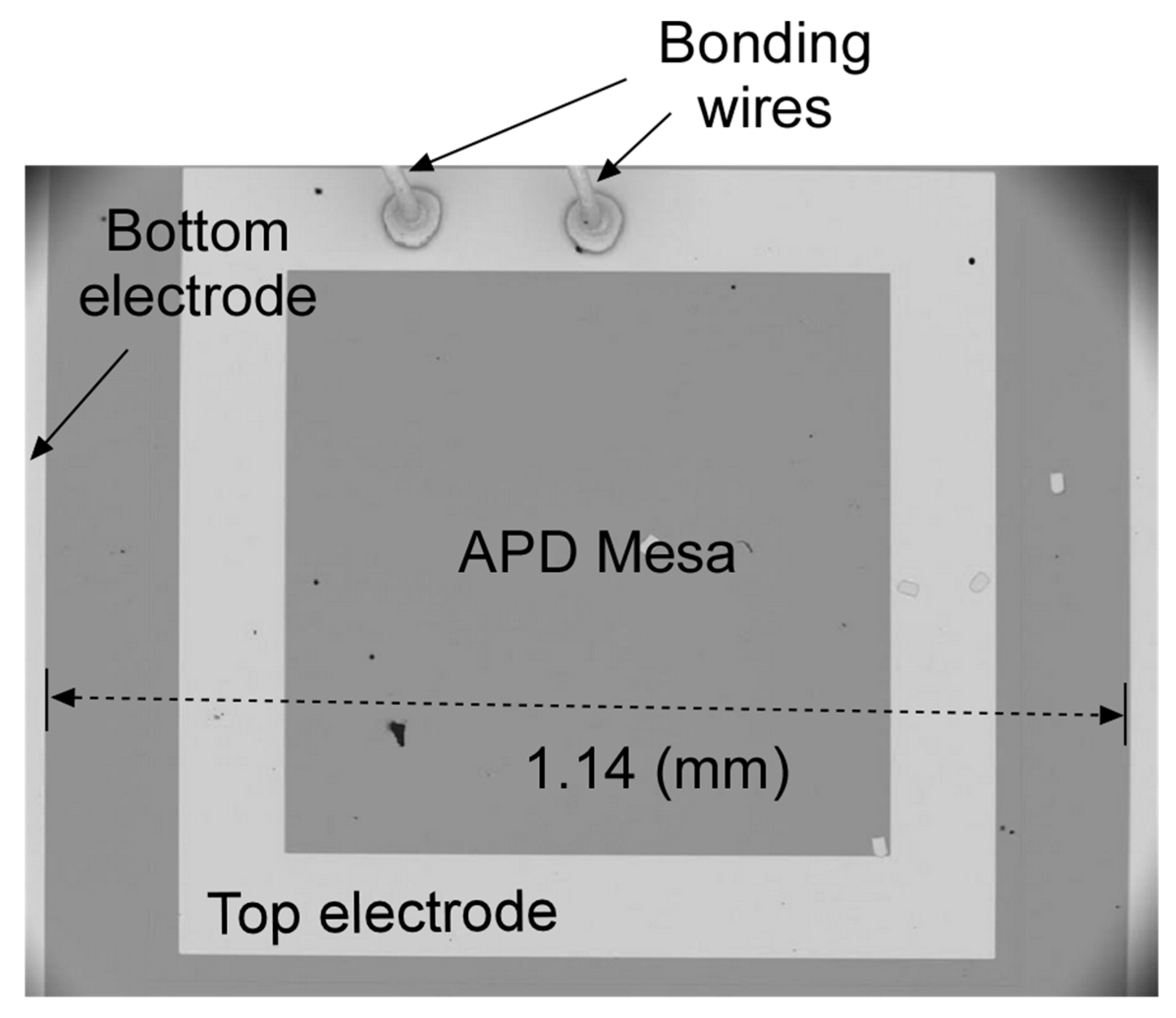
2. Device Structures, Material Growth, and the Device Fabrication

Figure 1 shows a cross-sectional, layer-by-layer diagram of the new In0.3Ga0.7As0.25Sb0.75/GaSb heterostructure e-SWIR APD. It consists of, from bottom (i.e., GaSb substrate) to top, n ( 5.0 × 10 18 / c m 3 ) tellurium (Te)-doped GaSb substrate, a 300 nanometer (nm) thick n + ( 2.0 × 10 19 / c m 3 ) Te-doped contacting layer, an undoped 500 nm In0.3Ga0.7As0.25Sb0.75 active absorption layer, a p- ( 1.5 × 10 17 / c m 3 ) beryllium (Be)-doped GaSb layer, an undoped GaSb layer (i-GaSb) as the avalanche region, and the p + ( 3.0 × 10 18 / c m 3 ) GaSb top contacting layer. The thickness of each layer is marked in the figure. The wider bandgap i-GaSb region was designed as the avalanche region to reduce dark current- and carrier generation/recombination (GR)-induced noise, thereby lowering both dark current and noise levels during the avalanche process [17,30,31].
The In0.3Ga0.7As0.25Sb0.75/GaSb e-SWIR APD heterostructure was grown using a Veeco GEN Xplor Molecular Beam Epitaxy (MBE) at Tufts University Epitaxy Core facility (TEC). The GaSb wafer was ramped up to a substrate temperature of 620 °C and kept at this temperature for 10 min to remove the native oxide layer. After the de-oxidization, the substrate temperature was reduced to 542 °C. The growth temperature was kept at 542 °C throughout the growth of the material. The growth rate for the In0.3Ga0.7As0.25Sb0.75 layer was 0.74 monolayers (ML) per second (i.e., 0.74 ML/s), and the growth rate for the GaSb layers was 0.52 ML/s. The growth rates were calibriated by reflection high-energy electron diffraction (RHEED) oscillation on the MBE machine right before the MBE growth, which ensured the accuracy of the layer thicknesses shown in Figure 1. Figure 2 shows the RHEED pattern after finishing the growth. The RHEED indicates high-quality lattice-matched In0.3Ga0.7As0.25Sb0.75/GaSb heterostructure growth on the GaSb substrate. The RHEED paterns were monitored throughout the material’s growth period to ensure lattice-matching was achieved for all the layers.
After the MBE growth, the wafer was processed into 1.1 mm × 1.1 mm square mesas using standard photolithography, inductively coupled plasma (ICP) etching, electron-beam (E-beam) metal deposition, and lift-off procedures. The ICP etching parameters were: BCl3, 10 standard cubic centimeters per minute (sccm), H2 5 sccm, 500 W ICP, 100 W RF, and a pressure of 2 millitorrs. The total etch depth was 850 nm, with a total etch time of 9 min 30 s. The top and bottom contacts were 20 nm titanium (Ti) and 300 nm gold (Au), deposited using the E-beam metal deposition and lift-off processes. Figure 3 shows a scanning electron microscope (SEM) image of the fabricated e-SWIR APD with a square mesa and bonding wires on the top electrode.

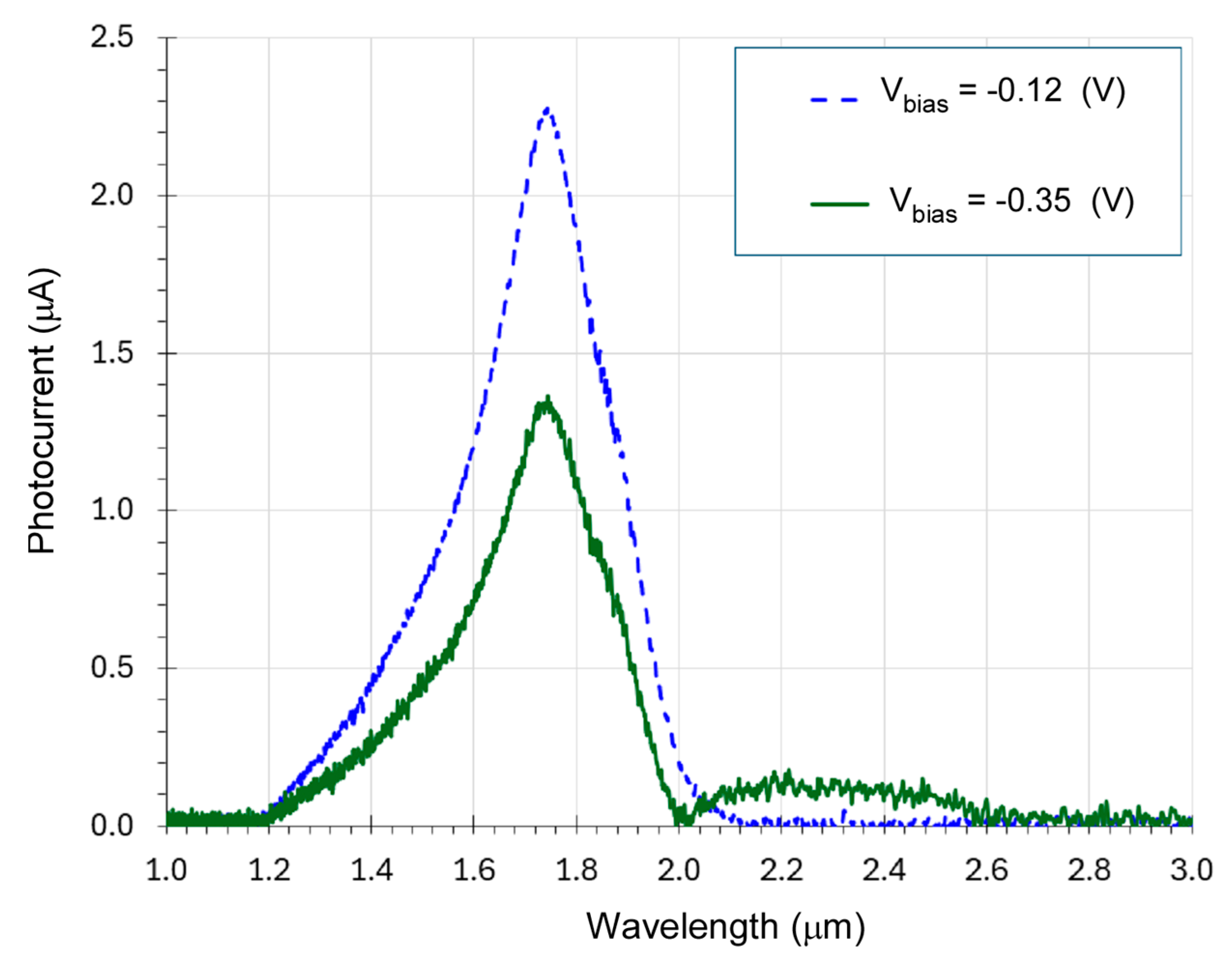
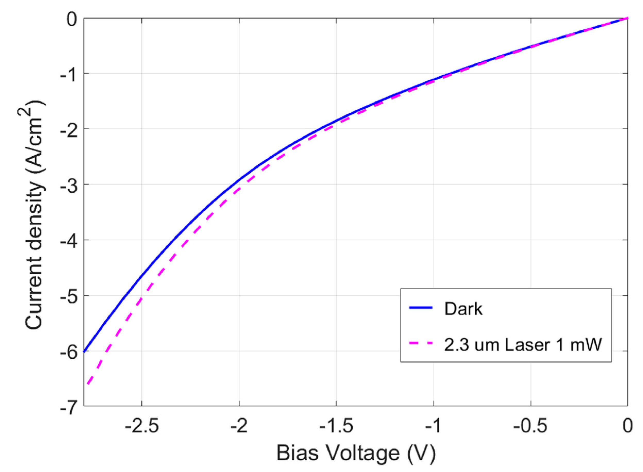
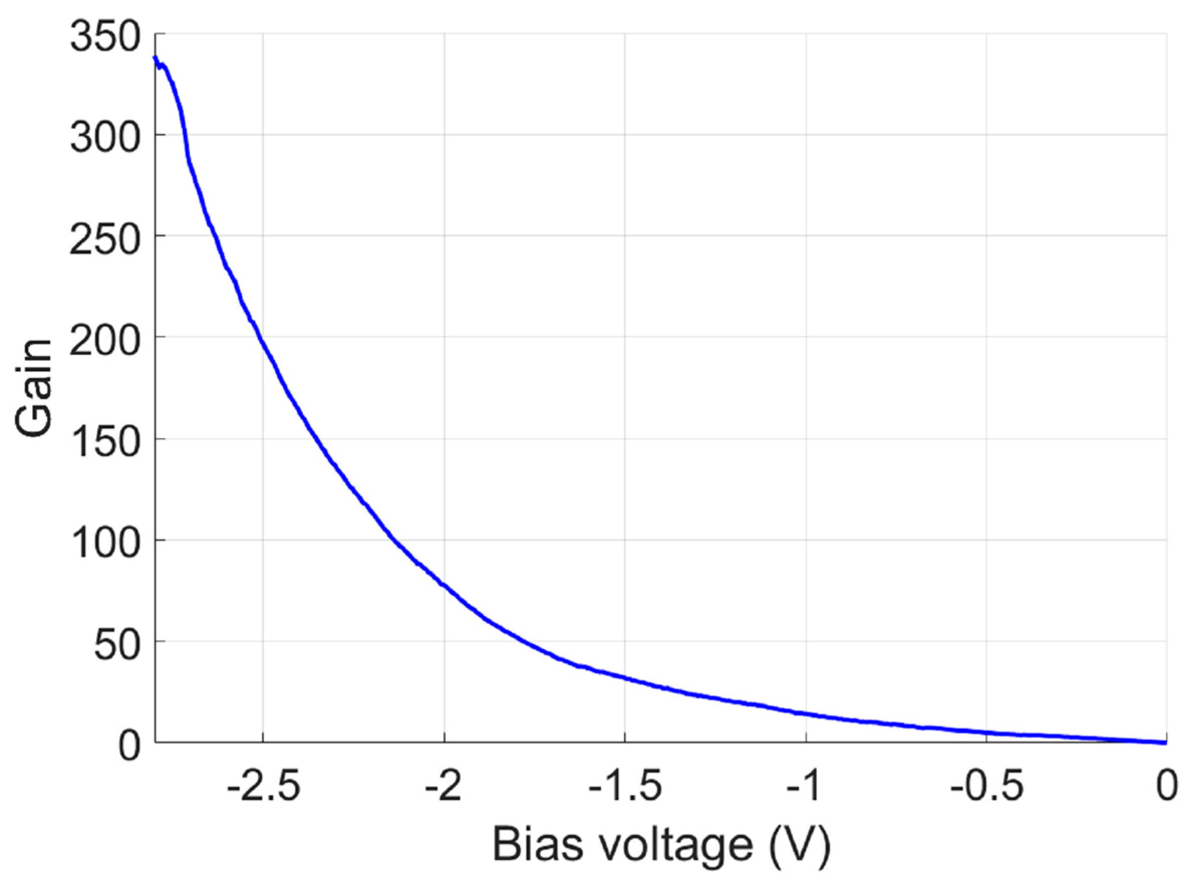
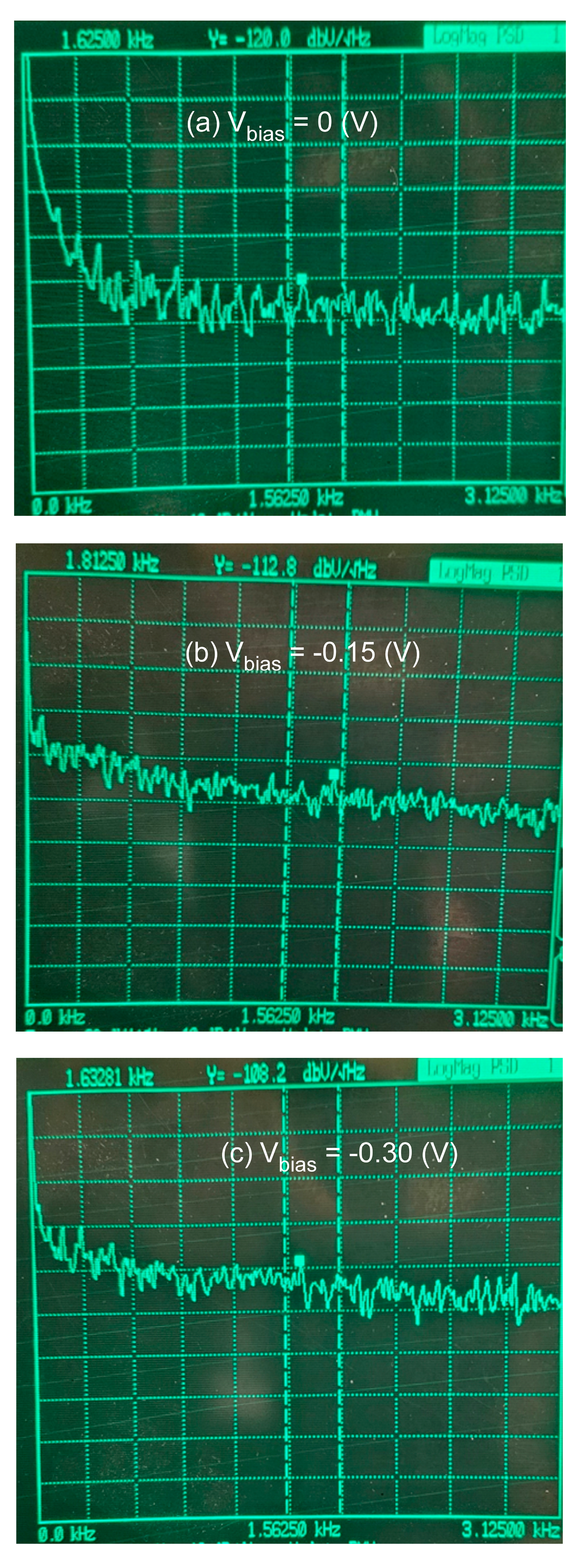
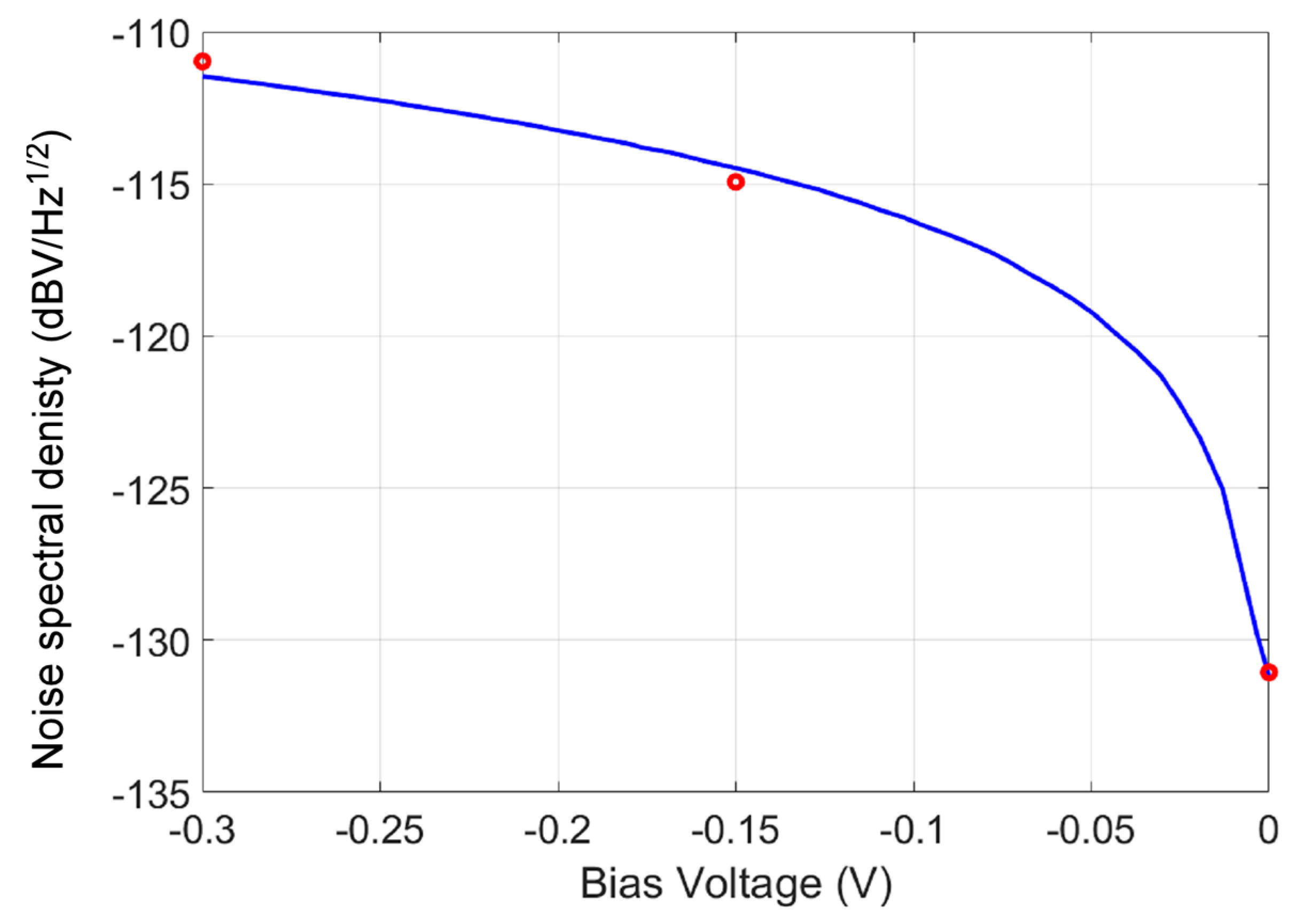
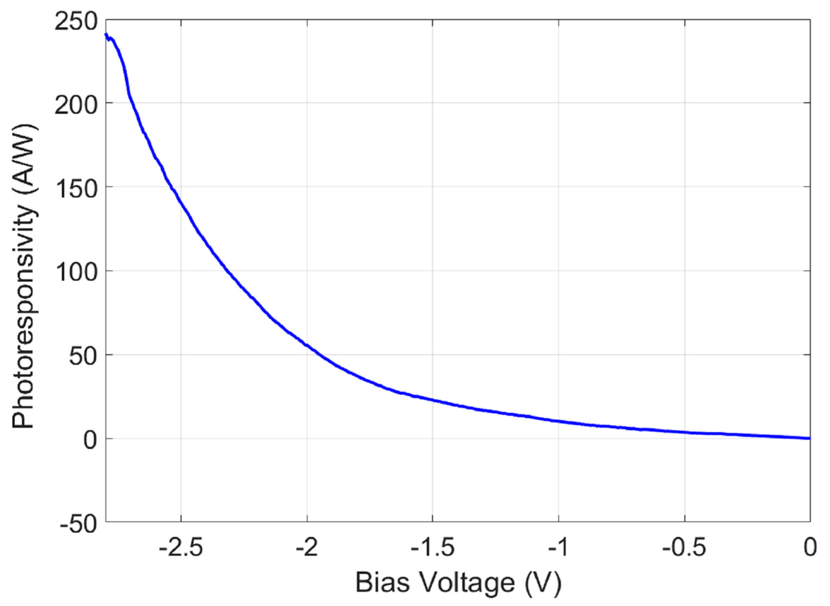
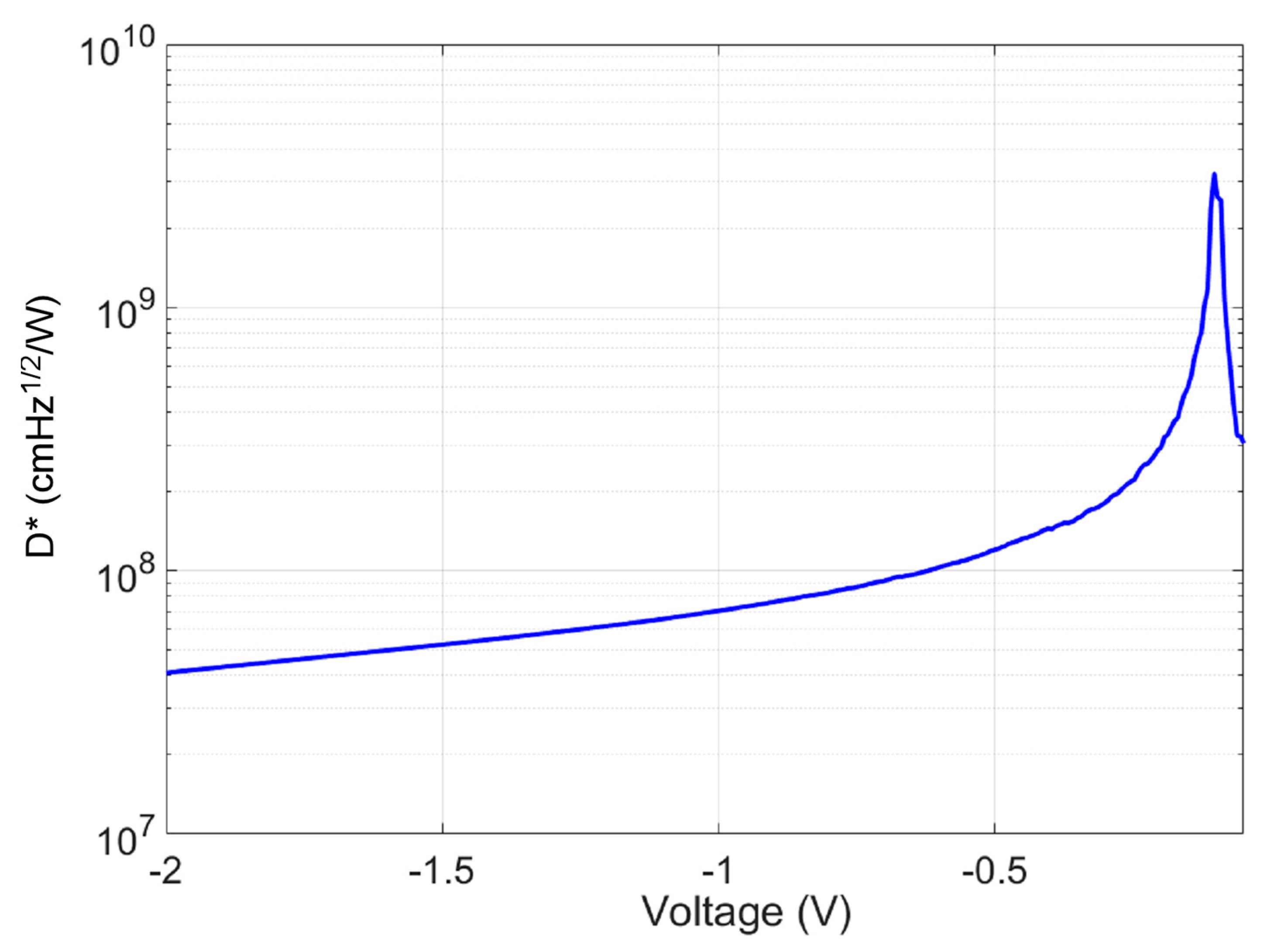
3. Results and Discussions

The photocurrent spectra of the fabricated e-SWIR APD, referred to henceforth as the device, were measured using a Bruker INVENIO® Fourier transform infrared (FTIR) spectrometer by Bruker Corporation at 40 Manning Rd, Billerica, MA, USA. The device replaced the internal DTGS detector of the FTIR, and the photocurrent signals were collected and transmitted to the FTIR through the equipment’s external A/D converter unit. The device was tested through top-illumination from the surface-normal direction. The device was not polished on the backside. The spot size of the FTIR illumination light was estimated to be 2 mm in diameter. Figure 4 displays the measured FTIR photocurrent spectra at different bias voltages. At a low bias voltage V b i a s = 0.12 (V) (dashed curve), the photocurrent spectra were primarily below the cutoff wavelength of a typical GaSb photodetector at 1.72 µm. Conversely, at a slightly higher bias voltage of V b i a s = 0.35 (V) (solid curve), the device exhibited a longer detection wavelength with a cutoff wavelength of λ c u t o f f = 2.6   μ m . This corresponded to the collection of the photocurrent generated in the In0.3Ga0.7As0.25Sb0.75 layer under the higher bias voltage. Note that the low-noise preamplifier used with the FTIR spectrometer had a low current overflow level, preventing the measurement of the photocurrent at higher biases. Nevertheless, the long cutoff wavelength of λ c u t o f f = 2.6   μ m at a low bias voltage of V b i a s = 0.35 (V) still demonstrated the APD’s capabilities in achieving the long cutoff wavelength of λ c u t o f f = 2.6   μ m at RT.
Note that the photocurrent was nearly zero at a wavelength of 2.6 µm, with a bias of V b i a s = 0.35 V. This occurred due to the electron band filling effect, also known as the Moss–Burstein effect [32,33,34], where the bias voltage shifts the Fermi-level and thus changes the occupations of the conduction bands and valence band. Similar phenomena have previously been reported and analyzed [35].
To obtain the photoresponse at higher bias voltages, the current versus bias voltage characteristics (i.e., I–V curves) of the APD were measured under the illumination of a distributed feedback (DFB) semiconductor laser (Eblana Photonics® EP2327) by Eblana Photonics at 3 West Pier Campus, Dun Laoghaire, Co. Dublin, A96 A621, Ireland with an emission wavelength of λ l a s e r = 2327   n m (referred to henceforth as the 2.3 µm laser) from the top illumination. Figure 5 shows the measured I–V curve under laser illumination (dashed curve) compared to the dark I–V curve (solid curve) without laser illumination. The APD-received laser power was estimated to be P r = 41   μ W . The photocurrent under 2.3 µm laser illumination confirmed the APD’s ability to detect IR light wavelengths exceeding 2.0 µm. Additionally, the steep slopes of the I–V curves at higher bias voltages than V b i a s < 1.5 (V) indicated the avalanche gain-induced high current. The avalanche process at the low bias voltage was attributed to the stepwise heterojunction design [29], which reduced the depletion width and thus led to a low breakdown voltage. It may have also been due to the breakdown at the sharp edges of the device.
To obtain the avalanche gains and the excess noise factor, we analyzed the noise components and the measured noise of the APD under different biases. The thermal noise current spectral density i t h / B in A / H z can be expressed as:
i t h / B = 4 k B T R d
where k B is the Boltzmann’s constant, T is the absolution temperature in kelvin (°K), and R d is the differential resistance of the APD, which can be calculated from the I-V characteristics shown in Figure 3. The shot noise current spectral density i s h / B in A / H z can be written as [36]:
i s h / B = 2 q M 2 I p h + I d | 0 F ( M )
where M is the avalanche gain; q = 1.6 × 10 19 (C) is the amount of charge of an electron; and the I p h + I d | 0 term is the sum of the photocurrent ( I p h ) and dark current ( I d ) before avalanche. F ( M ) is the excess noise factor, which can be expressed as follows for the hole-dominated impact ionization process [36]:
F M = k M + ( 1 k ) M M 1 M 2
where k = β / α represents the ratio of the impact ionization coefficient for holes, β , to that for electrons, α . The thermal noise current spectral density i t h / B was calculated to be ~ 2 × 10 11 A / H z , whereas the shot noise current spectral density was > ~ 1 × 10 10 A / H z , even at the avalanche gain of M = 1 . This indicates that the APD was shot-noise-dominated. The avalanche multiplication gain M was calculated using the following equation:
M = I p h I d | A v a l a n c h e I p h I d | 0
where I p h I d | A v a l a n c h e is the avalanched APD photocurrent and I p h I d | 0 is the photocurrent before the avalanche. Figure 6 shows the avalanche gain M at different bias voltages. A high gain of M ~ 190 was achieved at the bias voltage of V b i a s = 2.5 (V).
The temporal response was determined by the RC constant of the e-SWIR APD, which was calculated to be ~ 40 nanoseconds (ns).
The noise spectral density V S D d B V in d B V / H z of the device was measured using an SR770 FFT spectrum analyzer from Stanford Research Systems at 1290-D Reamwood Ave. Sunnyvale, CA, USA after converting the current signal to a voltage signal through a low-noise transimpedance preamplifier. Figure 7a, Figure 7b, and Figure 7c show the measured VSD at the bias voltages of 0 (V), −0.15 (V), and −0.30 (V), respectively. The measured VSD were − 120.0   d B V / H z , − 112.8   d B V / H z , and − 108.2   d B V / H z , respectively. The noise VSD of − 120.0   d B V / H z at the bias voltage of V b i a s = 0 (V) included the noise floor of the measurement equipment and was, thus, higher than the real VSD of the device.
The VSD in d B V / H z was related to the noise spectral density i s h / B by:
V S D d B V = 20 l o g 10 i s h S / B 1 V / B
Combining Equations (2)–(5), it was possible to calculate the VSD at different bias voltages and obtain the k factor value through curve-fitting with the measured VSD values. Figure 7 shows the calculated VSD at different bias voltages. The measured VSD values are marked in Figure 8 using circles. Note that the measured VSD values were adjusted by removing the noise floor of the equipment. The k factor value was determined to k = 0.003 by curve fitting.
The photoresponsivity R was defined as [37]:
R = I p h P r
where I p h is the photocurrent and P r is the laser power received by the device. Figure 9 shows the photoresponsivity R at different bias voltages.
The noise equivalent power (NEP) in W / H z was defined as [37]:
N E P = i n o i s e R
i n o i s e is the calculated current noise using the k factor value of k = 0.003 . Figure 10 shows the NEP at different bias voltages.
The specific photodetectivity (D*) in c m H z / W was defined as [37]:
D * = A N E P
where A is the area of the APD. Figure 11 shows the D* at different biases. The reverse bias increases caused a rise in noise level, resulting in a decrease in D*.

4. Conclusions

In conclusion, herein, an RT e-SWIR APD with a cutoff wavelength of 2.6 µm is demonstrated based on the In0.3Ga0.7As0.25Sb0.75/GaSb heterostructures lattice-matched on GaSb substrates with high material quality. The e-SWIR APD shows a high multiplication gain of M ~ 190 at a low bias of V b i a s = 2.5   V . The high internal gain enabled highly sensitive e-SWIR photodetection. The capability for RT operation eliminated the need for cooling, thus facilitating remote chemical sensing and infrared (IR) imaging with significantly reduced SWaP.

Author Contributions

Conceptualization, X.L.; methodology, M.B., G.G.; investigation, G.G, A.Z.S., B.X., C.H.D. and Y.X.; resources, R.J.A. and R.N.; data curation, M.B.; writing—original draft, X.L.; supervision, X.L., G.G. and Y.L.; project administration, X.L. and G.G.; funding acquisition, Ramaswamy Nagarajan. All authors have read and agreed to the published version of the manuscript.

Funding

The research was partially funded by the Army DEVCOM through HEROES under contract No. W911QY-18-2-0006-UA-2.

Data Availability Statement

The raw data supporting the conclusions of this article will be made available by the authors on request.

Acknowledgments

The device structure was grown using a Veeco GEN Xplor MBE at the Tufts University Epitaxy Core facility (TEC), with special thanks to John H. McElearney, Jr. for his assistance. Fabrication was completed at UMass Lowell’s Core Research Facility (CRF), and FTIR measurements were conducted at Stonehill College’s LEAP Integrated Photonics Center. The authors appreciate the valuable discussions with John Paul Kruszewski of Army DEVCOM Soldier Center, Claire Lepont of UMass Lowell HEROES, and Tricia Chigan of UMass Lowell’s Department of Electrical and Computer Engineering.

Conflicts of Interest

Xuejun Lu is also a co-founder of Applied NanoFemto Technologies LLC, 181 Stedman St. #, Lowell MA 01851. The authors declare no financial interests in the subject matter or materials presented in this paper.

References

  1. Liu, L.; Rabinowitz, J.; Bianconi, S.; Park, M.-S.; Mohseni, H. Highly sensitive SWIR detector array based on nanoscale phototransistors integrated on CMOS readout. Appl. Phys. Lett. 2020, 117, 191102. [Google Scholar] [CrossRef]
  2. Wen, M.; Wei, L.; Zhuang, X.; He, D.; Wang, S.; Wang, Y. High-sensitivity short-wave infrared technology for thermal imaging. Infrared Phys. Technol. 2018, 95, 93–99. [Google Scholar] [CrossRef]
  3. Hinds, S.; Klem, E.; Gregory, C.; Hilton, A.; Hames, G.; Violette, K. Extended SWIR High Performance and High Definition Colloidal Quantum Dot Imagers; SPIE: Bellingham, WA, USA, 2020; Volume 11407. [Google Scholar]
  4. Treps, N. Surpassing the Standard Quantum Limit for Optical Imaging Using Nonclassical Multimode Light. Phys. Rev. Lett. 2002, 88, 203601. [Google Scholar] [CrossRef] [PubMed]
  5. Pooser, R.C.; Lawrie, B. Plasmonic Trace Sensing below the Photon Shot Noise Limit. ACS Photonics 2016, 3, 8–13. [Google Scholar] [CrossRef]
  6. Lee, C.; Lawrie, B.; Pooser, R.; Lee, K.-G.; Rockstuhl, C.; Tame, M. Quantum Plasmonic Sensors. Chem. Rev. 2021, 121, 4743–4804. [Google Scholar] [CrossRef] [PubMed]
  7. Arslan, Y.; Oguz, F.; Besikci, C. Extended wavelength SWIR InGaAs focal plane array: Characteristics and limitations. Infrared Phys. Technol. 2015, 70, 134–137. [Google Scholar] [CrossRef]
  8. Martinelli, R.U.; Zamerowski, T.J.; Longeway, P.A. 2.6 μm InGaAs photodiodes. Appl. Phys. Lett. 1988, 53, 989–991. [Google Scholar] [CrossRef]
  9. Linga, K.R.; Olsen, G.H.; Ban, V.S.; Joshi, A.N.; Kosonocky, W.F. Dark current analysis and characterization of In/sub x/Ga/sub 1-x/As/InAs/sub y/P/sub 1-y/ graded photodiodes with x>0.53 for response to longer wavelengths (>1.7 mu m). J. Light. Technol. 1992, 10, 1050–1055. [Google Scholar] [CrossRef]
  10. Olsen, G.; Lange, M.; Cohen, M.; Kim, D.-S.; Forrest, S. Three-Band 1.0–2.5 um Near-Infrared InGaAs Detector Array; SPIE: Bellingham, WA, USA, 1994; Volume 2225. [Google Scholar]
  11. Zimmermann, L.; John, J.; Degroote, S.; Borghs, G.; Hoof, C.V.; Nemeth, S. Extended wavelength InGaAs on GaAs using InAlAs buffer for back-side-illuminated short-wave infrared detectors. Appl. Phys. Lett. 2003, 82, 2838–2840. [Google Scholar] [CrossRef]
  12. Ting, D.Z.-Y.; Hill, C.J.; Soibel, A.; Keo, S.A.; Mumolo, J.M.; Nguyen, J.; Gunapala, S.D. A high-performance long wavelength superlattice complementary barrier infrared detector. Appl. Phys. Lett. 2009, 95, 023508. [Google Scholar] [CrossRef]
  13. Youngdale, E.R.; Meyer, J.R.; Hoffman, C.A.; Bartoli, F.J.; Grein, C.H.; Young, P.M.; Ehrenreich, H.; Miles, R.H.; Chow, D.H. Auger lifetime enhancement in InAs–Ga1−xInxSb superlattices. Appl. Phys. Lett. 1994, 64, 3160–3162. [Google Scholar] [CrossRef]
  14. Delaunay, P.Y.; Nguyen, B.M.; Hoffman, D.; Huang, E.K.W.; Razeghi, M. Background Limited Performance of Long Wavelength Infrared Focal Plane Arrays Fabricated From M-Structure InAs–GaSb Superlattices. IEEE J. Quantum Electron 2009, 45, 157–162. [Google Scholar] [CrossRef]
  15. Nguyen, B.-M.; Hoffman, D.; Delaunay, P.-Y.; Razeghi, M. Dark current suppression in type II InAs∕GaSb superlattice long wavelength infrared photodiodes with M-structure barrier. Appl. Phys. Lett. 2007, 91, 163511. [Google Scholar] [CrossRef]
  16. Cohen-Elias, D.; Uliel, Y.; Klin, O.; Snapi, N.; Weiss, E.; Shafir, I.; Westreich, O.; Katz, M. Short wavelength infrared InAs/InSb/AlSb type-II superlattice photodetector. Infrared Phys. Technol. 2017, 84, 82–86. [Google Scholar] [CrossRef]
  17. Jones, A.H.; March, S.D.; Bank, S.R.; Campbell, J.C. Low-noise high-temperature AlInAsSb/GaSb avalanche photodiodes for 2-μm applications. Nat. Photonics 2020, 14, 559–563. [Google Scholar] [CrossRef]
  18. Savich, G.R.; Sidor, D.E.; Du, X.; Wicks, G.W.; Debnath, M.C.; Mishima, T.D.; Santos, M.B.; Golding, T.D.; Jain, M.; Craig, A.P.; et al. III–V semiconductor extended short-wave infrared detectors. J. Vac. Sci. Technol. B 2017, 35, 02B105. [Google Scholar] [CrossRef]
  19. Wicks, G.; Golding, T.; Jain, M.; Savich, G.; Sidor, D.; Du, X.; Debnath, M.; Mishima, T.; Santos, M. Extended-Shortwave Infrared Unipolar Barrier Detectors; SPIE: Bellingham, WA, USA, 2015; Volume 9370. [Google Scholar]
  20. Leemans, J.; Pejović, V.; Georgitzikis, E.; Minjauw, M.; Siddik, A.B.; Deng, Y.-H.; Kuang, Y.; Roelkens, G.; Detavernier, C.; Lieberman, I.; et al. Colloidal III–V Quantum Dot Photodiodes for Short-Wave Infrared Photodetection. Adv. Sci. 2022, 9, 2200844. [Google Scholar] [CrossRef]
  21. Miao, Y.; Lin, H.; Li, B.; Dong, T.; He, C.; Du, J.; Zhao, X.; Zhou, Z.; Su, J.; Wang, H.; et al. Review of Ge(GeSn) and InGaAs Avalanche Diodes Operating in the SWIR Spectral Region. Nanomaterials 2023, 13, 606. [Google Scholar] [CrossRef]
  22. Tran, H.; Pham, T.; Du, W.; Zhang, Y.; Grant, P.C.; Grant, J.M.; Sun, G.; Soref, R.A.; Margetis, J.; Tolle, J.; et al. High performance Ge0.89Sn0.11 photodiodes for low-cost shortwave infrared imaging. J. Appl. Phys. 2018, 124, 013101. [Google Scholar] [CrossRef]
  23. Eales, T.D.; Marko, I.P.; Schulz, S.; O’Halloran, E.; Ghetmiri, S.; Du, W.; Zhou, Y.; Yu, S.-Q.; Margetis, J.; Tolle, J.; et al. Ge1−xSnx alloys: Consequences of band mixing effects for the evolution of the band gap Γ-character with Sn concentration. Sci. Rep. 2019, 9, 14077. [Google Scholar] [CrossRef]
  24. Dong, Y.; Wang, W.; Lee, S.Y.; Lei, D.; Gong, X.; Loke, W.K.; Yoon, S.F.; Liang, G.; Yeo, Y.C. Avalanche photodiode featuring Germanium-tin multiple quantum wells on silicon: Extending photodetection to wavelengths of 2 and beyond. In Proceedings of the 2015 IEEE International Electron Devices Meeting (IEDM), Washington, DC, USA, 7–9 December 2015; pp. 30.35.31–30.35.34. [Google Scholar]
  25. Yang, J.; Hu, H.; Miao, Y.; Wang, B.; Wang, W.; Su, H.; Ma, Y. Single-crystalline GePb alloys formed by rapid thermal annealing-induced epitaxy. J. Phys. D Appl. Phys. 2020, 53, 265105. [Google Scholar] [CrossRef]
  26. Besikci, C. Extended Short Wavelength infrared FPA Technology: Status and Trends; SPIE: Bellingham, WA, USA, 2018; Volume 10540. [Google Scholar]
  27. Olsen, G.; Joshi, A.; Mason, S.; Woodruff, K.; Mykietyn, E.; Ban, V.; Lange, M.; Hladky, J.; Erickson, G.; Gasparian, G. Room-Temperature InGaAs Detector Arrays for 2.5 µm; SPIE: Bellingham, WA, USA, 1990; Volume 1157. [Google Scholar]
  28. D’Souza, A.; Stapelbroek, M.; Dawson, L.; Ely, P.; Yoneyama, C.; Reekstin, J.; Skokan, M.; Kinch, M.; Liao, P.; Ohlson, M.; et al. SWIR to LWIR HDVIP HgCdTe Detector Array Performance; SPIE: Bellingham, WA, USA, 2006; Volume 6206. [Google Scholar]
  29. Wang, H.; Xia, H.; Liu, Y.; Chen, Y.; Xie, R.; Wang, Z.; Wang, P.; Miao, J.; Wang, F.; Li, T.; et al. Room-temperature low-threshold avalanche effect in stepwise van-der-Waals homojunction photodiodes. Nat. Commun. 2024, 15, 3639. [Google Scholar] [CrossRef] [PubMed]
  30. Dupuis, R.D.; Velebir, J.R.; Campbell, J.C.; Qua, G.J. Avalanche photodiodes with separate absorption and multiplication regions grown by metalorganic vapor deposition. IEEE Electron Device Lett. 1986, 7, 296–298. [Google Scholar] [CrossRef]
  31. Li, J.; Dehzangi, A.; Brown, G.; Razeghi, M. Mid-wavelength infrared avalanche photodetector with AlAsSb/GaSb superlattice. Sci. Rep. 2021, 11, 7104. [Google Scholar] [CrossRef] [PubMed]
  32. Moss, T.S. The Interpretation of the Properties of Indium Antimonide. Proc. Phys. Society Sect. B 1954, 67, 775–782. [Google Scholar] [CrossRef]
  33. Burstein, E. Anomalous Optical Absorption Limit in InSb. Phys. Rev. 1954, 93, 632–633. [Google Scholar] [CrossRef]
  34. Ghezzi, C.; Magnanini, R.; Parisini, A.; Rotelli, B.; Tarricone, L.; Bosacchi, A.; Franchi, S. Concentration dependence of optical absorption in tellurium-doped GaSb. Semicond. Sci. Technol. 1997, 12, 858–866. [Google Scholar] [CrossRef]
  35. Xiang, B.; Gu, G.; Ramaswamyd, N.; Drew, C.; Lu, X. Voltage-dependent extended shortwave infrared (e-SWIR) photodetection-band tuning utilizing the Moss–Burstein effect. J. Phys. D Appl. Phys. 2023, 56, 055101. [Google Scholar] [CrossRef]
  36. McIntyre, R.J. Multiplication noise in uniform avalanche diodes. IEEE Trans. Electron Devices 1966, ED-13, 164–168. [Google Scholar] [CrossRef]
  37. Sze, S.M.; Ng, K.K. Physics of Semiconductor Devices; Wiley: Hoboken, NJ, USA, 2006. [Google Scholar]
Figure 1. Layer-by-layer structure of the In0.3Ga0.7As0.25Sb0.75/GaSb e-SWIR APD.
Micromachines 15 00941 g001
Figure 2. RHEED pattern after the growth was finished.
Micromachines 15 00941 g002
Figure 3. SEM image of the e-SWIR APD with bonding wires on the top electrode.
Micromachines 15 00941 g003
Figure 4. Measured FTIR photocurrent spectra of the APD at different reverse biases. At V b i a s = 0.12 (V) (dashed curve), the photocurrent spectrum was mainly below the cutoff wavelength of 2.0 µm, whereas at a higher bias of V b i a s = 0.35 (V) (solid curve), the photocurrent spectrum was extended to a longer cutoff wavelength of 2.6 µm.
Micromachines 15 00941 g004
Figure 5. Measured I–V curve (dashed curve) of the APD under 2.3 µm laser illumination compared to the dark I–V curve (solid curve).
Micromachines 15 00941 g005
Figure 6. Calculated avalanche gain of the device under different voltage biases.
Micromachines 15 00941 g006
Figure 7. Measured VSD of the APD under different voltage biases.
Micromachines 15 00941 g007
Figure 8. Calculated VSD values at different bias voltages (solid curve). The circles are the measured VSD values after noise floor adjustment.
Micromachines 15 00941 g008
Figure 9. Photoresponsivity R at different voltage biases.
Micromachines 15 00941 g009
Figure 10. Noise equivalent power (NEP) W / H z at different biases.
Micromachines 15 00941 g010
Figure 11. D* ( c m W / H z ) at different biases.
Micromachines 15 00941 g011
Table 1. Comparison of this e-SWIR APD with previously reported APDs.
Performance FeaturesThis WorkAlInAsSb/GaSb APD [17]Ge1−xSnx APD [24] Stepwise WSe2 APD [29]
Cutoff Wavelength (µm)2.62.02.003<1
Gain190>100>15>100
Operating Temperature RTRTRTRT
Reverse Bias (V)<2.5>20<10<1.6
K-Factor k ~ 0.003 k ~ 0.01 N/AN/A
Photoresponsivity (A/W) > 140 N/A0.33N/A
Photodetectivity   D *   ( c m H z / W ) 3 × 10 7 N/AN/AN/A
N/A: Not reported in the reference.
Disclaimer/Publisher’s Note: The statements, opinions and data contained in all publications are solely those of the individual author(s) and contributor(s) and not of MDPI and/or the editor(s). MDPI and/or the editor(s) disclaim responsibility for any injury to people or property resulting from any ideas, methods, instructions or products referred to in the content.

