
Raman Investigation on Silicon Nitride Chips after Soldering onto Copper Substrates


Abstract
:1. Introduction
2. Materials and Methods
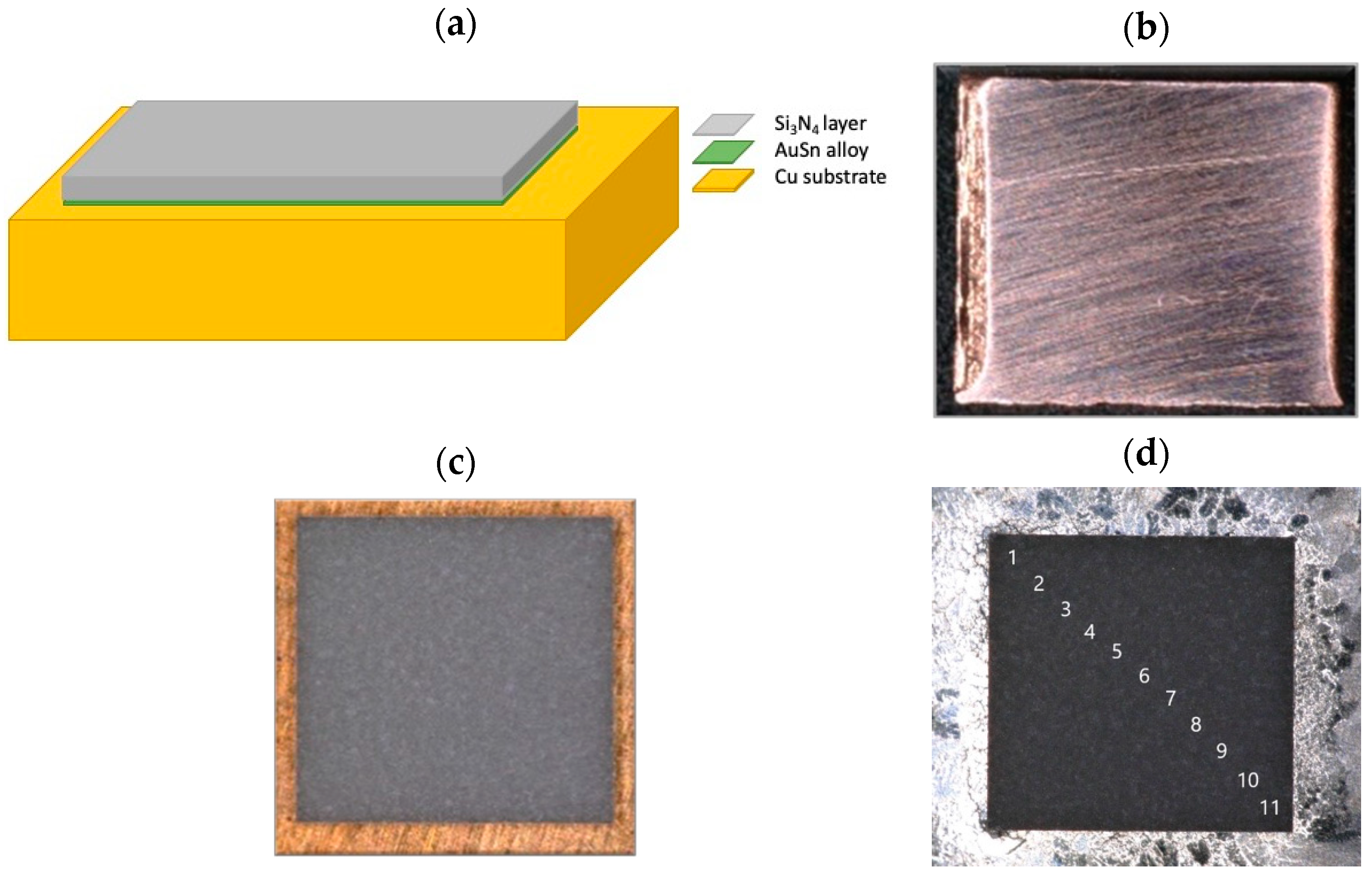
2.1. Substrates, Interconnections, and Chips
2.2. Samples
2.3. Methods
2.3.1. Micro-Raman Set-Up
2.3.2. Micro-Raman Acquisition Parameters
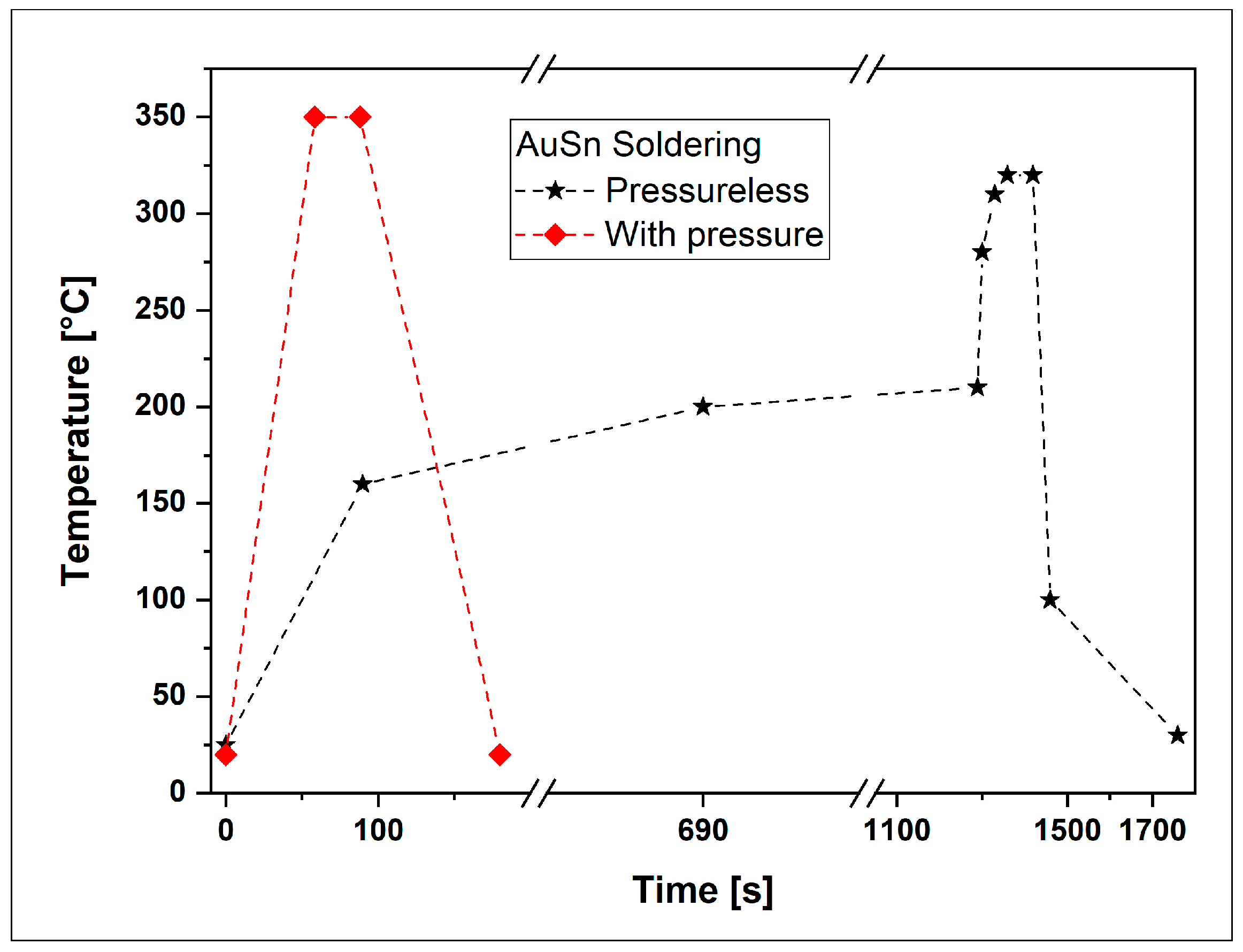
2.3.3. Sample Temperature Controlling
2.3.4. Calibration of Raman Spectra
2.3.5. Determination of Stress from Raman Spectra
3. Results
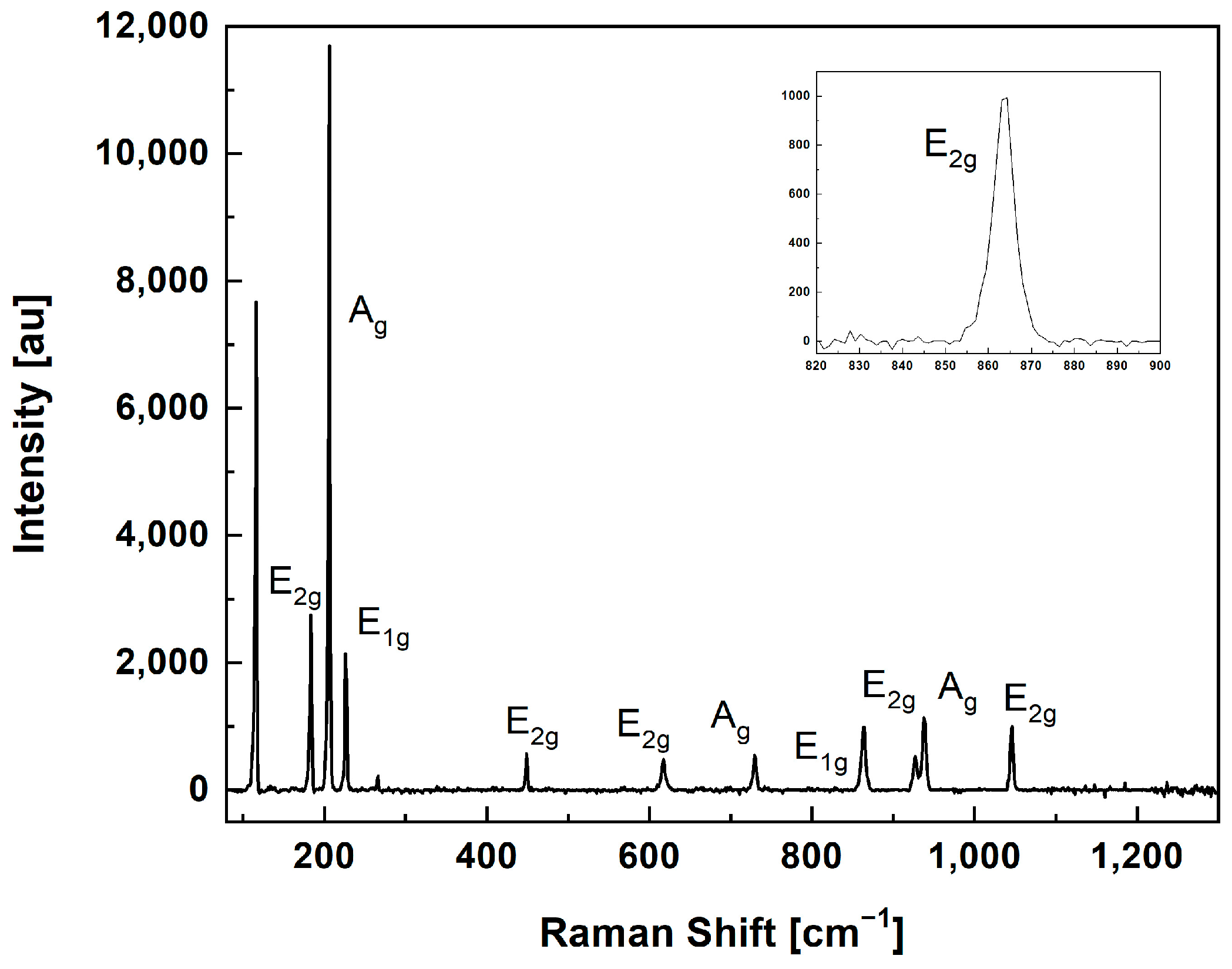
3.1. Raman Spectrum of Si3N4
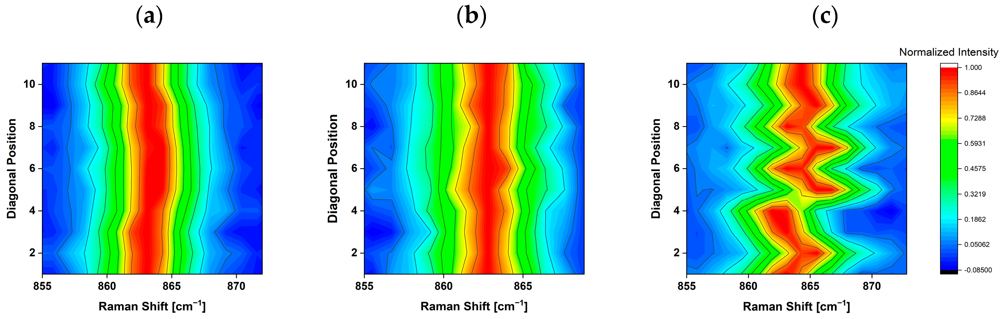
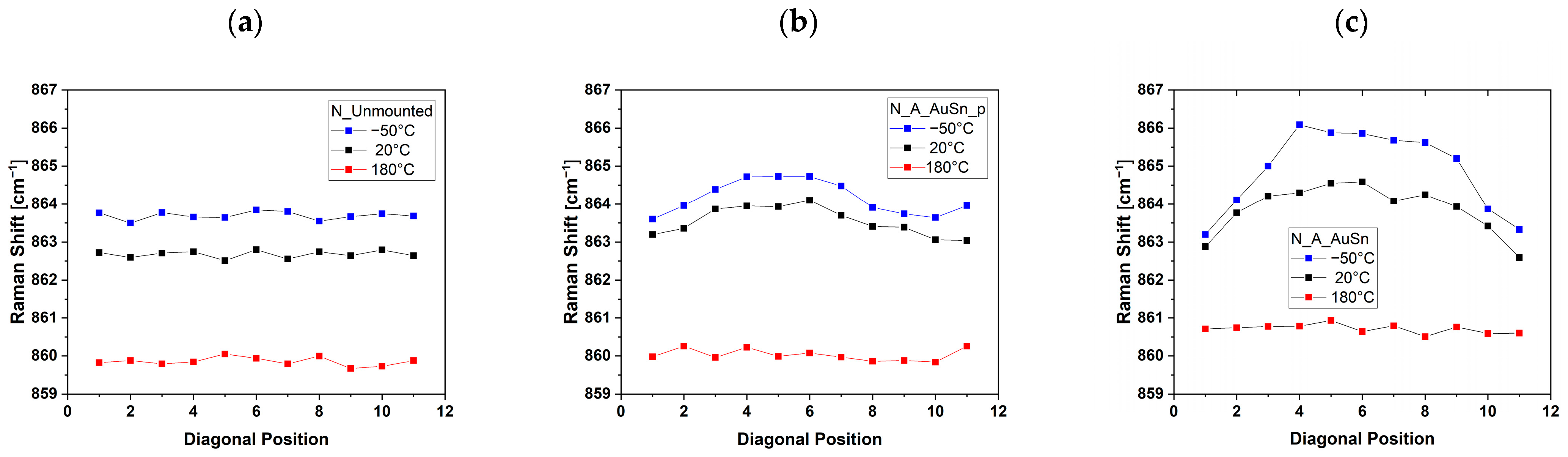
3.2. Behavior of Raman Signals along the Diagonal of the Samples
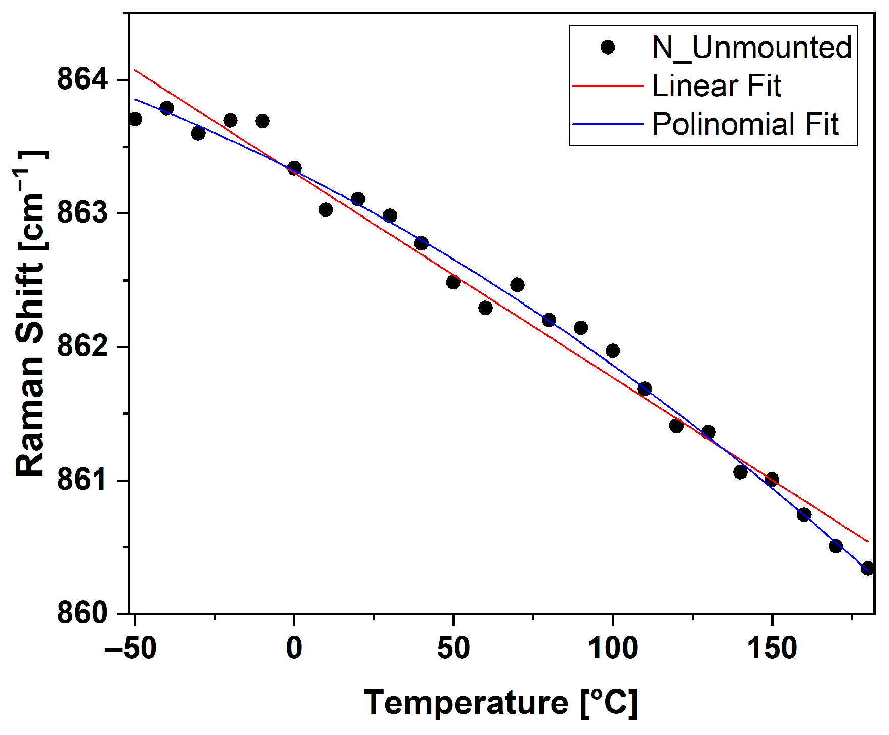
3.3. Effect of Temperature on Si3N4 Samples
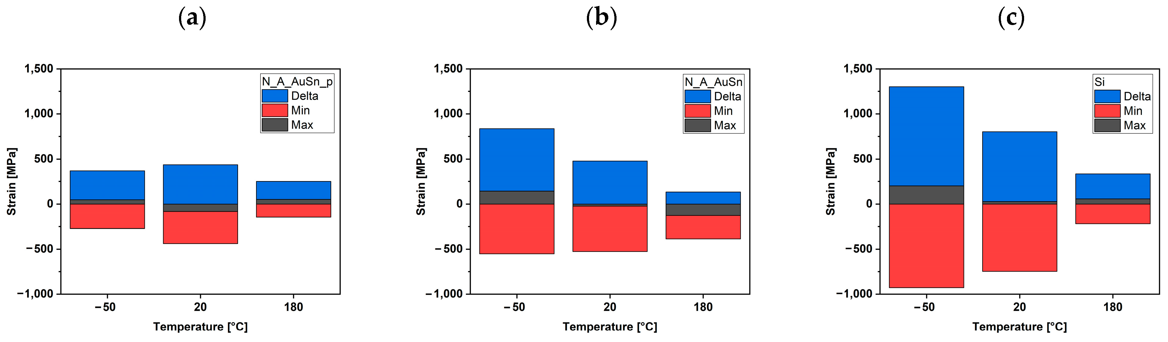
4. Discussion
5. Conclusions
Author Contributions
Funding
Data Availability Statement
Conflicts of Interest
References
- Villa, A.; Gianchandani, P.K.; Baino, F. Sustainable Approaches for the Additive Manufacturing of Ceramic Materials. Ceram. Mater. 2024, 7, 291–309. [Google Scholar] [CrossRef]
- Kawai, C.; Yamakawa, A. Effect of Porosity and Microstructure on the Strength of Si3N4: Designed Microstructure for High Strength, High Thermal Shock Resistance, and Facile Machining. J. Am. Ceram. Soc. 1997, 80, 2705–2708. [Google Scholar] [CrossRef]
- Vasiliev, V.Y. Composition, structure, and functional properties of thin silicon nitride films grown by atomic layer deposition for microelectronic applications. J. Struct. Chem. 2022, 63, 1019–1050. [Google Scholar] [CrossRef]
- Zhao, Y.; Dong, S.; Hu, P.; Zhao, X.; Hong, C. Recent progress in synthesis, growth mechanisms, properties, and applications of silicon nitride nanowire. Ceram. Int. 2021, 47, 14944–14965. [Google Scholar] [CrossRef]
- Kaloyeros, A.E.; Pan, Y.; Goff, J.; Arkles, B. Review—Silicon Nitride and Silicon Nitride-Rich Thin Film Technologies: State-of-the-Art Processing Technologies, Properties, and Applications. ECS J. Solid State Sci. Technol. 2020, 9, 063006. [Google Scholar] [CrossRef]
- Honda, K.; Yokoyama, S.; Tanaka, S.-I. Assignment of the Raman active vibration modes of β-Si3N4 using micro-Raman scattering. J. Appl. Phys. 1999, 85, 7380–7384. [Google Scholar] [CrossRef]
- Dong, J.; Sankey, O.F. Comment on “Assignment of the Raman active vibration modes of β-Si3N4 using micro-Raman scattering”. J. Appl. Phys. 2000, 87, 958–959. [Google Scholar] [CrossRef]
- Mashayekh, A.T.; Klos, T.; Geuzebroek, D.; Klein, E.; Veenstra, T.; Büscher, M.; Merget, F.; Lisching, P.; Witzens, G. Silicon nitride PIC-based multi-color laser engines for life science applications. Opt. Express 2021, 29, 8635–8653. [Google Scholar] [CrossRef] [PubMed]
- Heimann, R.B. Silicon Nitride, a Close to Ideal Ceramic Material for Medical Application. Ceramics 2021, 4, 208–223. [Google Scholar] [CrossRef]
- Heimann, R.B. Silicon Nitride Ceramics: Structure, Synthesis, Properties, and Biomedical Applications. Materials 2023, 16, 5142. [Google Scholar] [CrossRef]
- Porcel, M.A.G.; Hinojosa, A.; Jans, H.; Stassen, A.; Goyvaerts, J.; Geuzebroek, D.; Geiselmann, M.; Carlos Dominguez, C.; Artundo, I. Silicon nitride photonic integration for visible light applications. Opt. Laser Technol. 2019, 112, 299–306. [Google Scholar] [CrossRef]
- Su, Y.; Zhang, Y.; Qiu, C.; Guo, X.; Sun, L. Silicon Photonic Platform for Passive Waveguide Devices: Materials, Fabrication, and Applications. Adv. Mater. Technol. 2020, 5, 1901153. [Google Scholar] [CrossRef]
- Xiang, C.; Jin, W.; Bowers, J.E. Silicon nitride passive and active photonic integrated circuits: Trends and prospects. Photonics Res. 2022, 10, A82–A96. [Google Scholar] [CrossRef]
- Bocanegra-Bernal, M.H.; Matovic, B. Mechanical properties of silicon nitride-based ceramics and its use in structural applications at high temperatures. Mater. Sci. Eng. A 2010, 527, 1314–1338. [Google Scholar] [CrossRef]
- Blumenthal, D.J.; Heideman, R.; Geuzebroek, D.; Leinse, A.; Roeloffzen, C. Silicon Nitride in Silicon Photonics. Proc. IEEE 2018, 106, 2209–2231. [Google Scholar] [CrossRef]
- Aguayo-Alvarado, A.L.; Araiza-Sixtos, F.A.; Abundiz-Cisneros, N.; Rangel-Rojo, R.; Garay-Palmett, K.; De La Cruz, W. Linear and nonlinear properties study of silicon nitride films for integrated photonics. J. Non-Cryst. Solids 2023, 613, 122370. [Google Scholar] [CrossRef]
- Gardes, F.; Shooa, A.; De Paoli, G.; Skandalos, I.; Ilie, S.; Rutirawut, T.; Talataisong, W.; Faneca, J.; Vitali, V.; Hou, Y.; et al. A Review of Capabilities and Scope for Hybrid Integration Offered by Silicon-Nitride-Based Photonic Integrated Circuits. Sensors 2022, 22, 4227. [Google Scholar] [CrossRef] [PubMed]
- Sharma, T.; Wang, J.; Kaushik, B.K.; Cheng, Z.; Kumar, R.; Wei, Z.; Li, X. Review of Recent Progress on Silicon Nitride-Based Photonic Integrated Circuits. IEEE Access 2020, 8, 195436–195446. [Google Scholar] [CrossRef]
- Ma, C.; Hou, J.; Yang, C.Y.; Shi, M.; Chen, S.P. Complete photonic bandgap in a silicon nitride slab by utilizing the effective index difference between polarizations. Front. Optoelectron. 2022, 15, 20. [Google Scholar] [CrossRef]
- Steegena, A.; Maexa, K. Silicide-induced stress in Si: Origin and consequences for MOS technologies. Mater. Sci. Eng. R 2002, 38, 1–53. [Google Scholar] [CrossRef]
- Rymaszewski, E.J.; Tummala, R.R.; Watari, T. Microelectronics Packaging—An Overview. In Microelectronics Packaging Handbook; Tummala, R.R., Rymaszewski, E.J., Klopfenstein, A.G., Eds.; Springer: Boston, MA, USA, 1997. [Google Scholar] [CrossRef]
- Truong, T.-A.; Nguyen, T.-K.; Zhao, H.; Nguyen, N.-K.; Dinh, T.; Park, Y.; Nguyen, T.; Yamauchi, Y.; Nguyen, N.-T.; Phan, H.-P. Engineering Stress in Thin Films: An Innovative Pathway Toward 3D Micro and Nanosystems. Small 2022, 18, 2105748. [Google Scholar] [CrossRef] [PubMed]
- Ingrid De Wolf, I. Micro-Raman spectroscopy to study local mechanical stress in silicon integrated circuits. Semicond. Sci. Technol. 1996, 11, 139–154. [Google Scholar] [CrossRef]
- Takahiro Miyatake, T.; Pezzotti, G. Tensor-resolved stress analysis in silicon MEMS device by polarized Raman spectroscopy. Phys. Status Solidi A 2011, 208, 1151–1158. [Google Scholar] [CrossRef]
- Xu, Z.; He, Z.; Song, Y.; Fu, X.; Rommel, M.; Luo, X.; Hartmaier, A.; Zhang, J.; Fang, F. Topic Review: Application of Raman Spectroscopy Characterization in Micro/Nano-Machining. Micromachines 2018, 9, 361. [Google Scholar] [CrossRef]
- Liu, E.; Conti, F.; Bhogaraju, S.K.; Signorini, R.; Pedron, D.; Wunderle, B.; Elger, G. Thermomechanical stress in GaN-LEDs soldered onto Cu substrates studied using finite element method and Raman spectroscopy. J. Raman Spectrosc. 2020, 51, 2083–2094. [Google Scholar] [CrossRef]
- Nazari, M.; Holtz, M.W. Near-ultraviolet Raman and micro-Raman analysis of electronic materials. Appl. Phys. Rev. 2018, 5, 041303. [Google Scholar] [CrossRef]
- De Wolf, I.; Maes, H.E.; Jones, S.K. Stress measurements in silicon devices through Raman spectroscopy: Bridging the gap between theory and experiment. J. Appl. Phys. 1996, 79, 7148–7156. [Google Scholar] [CrossRef]
- Ma, L.; Qiu, W.; Fan, X. Stress/strain characterization in electronic packaging by micro-Raman spectroscopy: A review. Microelectron. Reliab. 2021, 118, 114045. [Google Scholar] [CrossRef]
- Yang, Z.; Wang, X.; Chen, W.; Tang, H.; Zhang, R.; Fan, X.; Zhang, G.; Fan, J. Residual Stress Characterization in Microelectronic Manufacturing: An Analysis Based on Raman Spectroscopy. Laser Photonics Rev. 2024, 18, 2301300. [Google Scholar] [CrossRef]
- Saringer, C.; Tkadletz, M.; Mitterer, C. Restrictions of stress measurements using the curvature method by thermally induced plastic deformation of silicon substrates. Surf. Coat. Technol. 2015, 274, 68–75. [Google Scholar] [CrossRef]
- Li, Q.; Qiu, W.; Tan, H.; Guo, J.-G.; Kang, Y. Micro-Raman spectroscopy stress measurement method for porous silicon film. Opt. Lasers Eng. 2010, 48, 1119–1125. [Google Scholar] [CrossRef]
- Kimoto, K.; Usami, K.; Sakata, H.; Tanaka, M. Measurement of Strain in Locally Oxidized Silicon using Convergent-Beam Electron Diffraction. Jpn. J. Appl. Phys. 1993, 32, 211–213. [Google Scholar] [CrossRef]
- Chen, C.; Sun, M.; Cheng, Z.; Liang, Y. Microstructure Evolution and Shear Strength of the Cu/Au80Sn20/Cu Solder Joints with Multiple Reflow Temperatures. Materials 2022, 15, 780. [Google Scholar] [CrossRef] [PubMed]
- Matijasevic, G.S.; Wang, C.Y.; Lee, C.C. Void Free Bonding of Large Silicon Dice Using Gold-Tin Alloys. IEEE Trans. Compon. Hybrids Manuf. Technol. 1990, 13, 1128–1134. [Google Scholar] [CrossRef]
- Elger, G.; Kandaswamy, S.V.; Von Kouwen, M.; Derix, R.; Conti, F. In-Situ measurements of the relative thermal resistance:Highly sensitive method to detect crack propagation in solder joints. In Proceedings—Electronic Components and Technology Conference; IEEE: Piscataway, NJ, USA, 2014; pp. 1464–1470. [Google Scholar] [CrossRef]
- Hanss, A.; Schmid, M.; Bhogaraju, S.K.; Conti, F.; Elger, G. Reliability of sintered and soldered high power chip size packages and flip chip LEDs. In Proceedings—Electronic Components and Technology Conference; IEEE: Piscataway, NJ, USA, 2018; pp. 2080–2088. [Google Scholar] [CrossRef]
- Signorini, R.; Pedron, D.; Conti, F.; Hanss, A.; Bhogaraju, S.K.; Elger, G. Thermomechanical Stress in GaN LED Soldered on Copper Substrate Evaluated by Raman Measurements and Computer Modelling. In Proceedings of the 24th International Workshop on Thermal Investigations of ICs and Systems, THERMINIC 2018—Proceedings, Stockholm, Sweden, 26–28 September 2018; p. 8593304. [Google Scholar] [CrossRef]
- Tochino, S.; Pezzotti, G. Micromechanical analysis of silicon nitride: A comparative study by fracture mechanics and Raman microprobe spectroscopy. J. Raman Spectrosc. 2002, 33, 709–714. [Google Scholar] [CrossRef]
- Sergo, V.; Pezzotti, G.; Ktagiri, G.; Muraki, N.; Nishida, T. Stress Dependence of the Raman Spectrum of β-Silicon Nitride. J. Am. Ceram. Soc. 1996, 79, 781–784. [Google Scholar] [CrossRef]
- Zhu, W.; Pezzotti, G. Raman analysis of three-dimensionally graded stress tensor components in sapphire. J. Appl. Phys. 2011, 109, 073502. [Google Scholar] [CrossRef]
- Loudon, R. The Raman Effect in Crystals. Adv. Phys. 2010, 50, 813–864. [Google Scholar] [CrossRef]
- Wada, N.; Solin, S.A.; Wong, J.; Prochazka, S. Raman and IR absorption spectroscopy studies on a, b and amorphous Si3N4. J. Non-Cryst. Solids 1981, 43, 7–15. [Google Scholar] [CrossRef]
- Brugnolotto, E.; Mezzalira, C.; Conti, F.; Pedron, D.; Signorini, R. Micro-Raman for Local Strain Evaluation of GaN LEDs and Si Chips Assembled on Cu Substrates. Micromachines 2024, 15, 25. [Google Scholar] [CrossRef]
- Peng, Y.; Hu, X.; Xu, X.; Chen, X.; Peng, J.; Han, J.; Dimitrijev, S. Temperature and doping dependence of the Raman scattering in 4H-SiC. Opt. Mater. Express 2016, 6, 2725–2733. [Google Scholar] [CrossRef]
- Li, W.S.; Shen, Z.X.; Feng, Z.C.; Chua, S.J. Temperature dependence of Raman scattering in hexagonal gallium nitride films. J. Appl. Phys. 2000, 87, 3332–3337. [Google Scholar] [CrossRef]
- Lucazeau, G. Effect of pressure and temperature on Raman spectra of solids: Anharmonicity. J. Raman Spectrosc. 2003, 34, 478–496. [Google Scholar] [CrossRef]
- Pecht, M. Handbook of Electronic Package Design (Dekker Mechanical Engineering); CRC Press: London, UK, 1991. [Google Scholar]
- Silicon Nitride (Si3N4) Properties and Applications. AZO Materials. Available online: https://www.azom.com/properties.aspx?ArticleID=53 (accessed on 28 July 2024).
- EngeneeringToolBox. Coefficients of Linear Thermal Expansion. 2003. Available online: https://www.engineeringtoolbox.com/linear-expansion-coefficients-d_95.html (accessed on 28 July 2024).
- Zhou, T.; Bobal, T.; Oud, M.A.; Songliang, J. Au-Sn Solder Alloy and Its Applications in Electronics Packaging; Coining Inc.: Montvale, NJ, USA, 2010; pp. 1–7. Available online: https://api.semanticscholar.org/CorpusID:35384046 (accessed on 28 July 2024).

| Duration mm:ss | Temperature [°C] | Ramp Rate [°C/s] | Cool | N2 | Formic Acid |
|---|---|---|---|---|---|
| 00:30 | 25 | 50 | off | on | off |
| 01:00 | 160 | 135 | off | off | on |
| 10:00 | 200 | 4 | off | off | on |
| 10:00 | 210 | 1 | off | off | on |
| 00:10 | 280 | 420 | off | off | on |
| 00:30 | 310 | 60 | off | off | on |
| 00:30 | 320 | 20 | off | off | on |
| 01:00 | 320 | 0 | off | off | on |
| 00:40 | 100 | −330 | on | on | off |
| 05:00 | 30 | −14 | on | on | off |
| Duration mm:ss | Temperature [°C] | Ramp Rate [°C/s] | Cool | N2 |
|---|---|---|---|---|
| 00:00 | 25 | 0 | off | off |
| 01:00 | 325 | 5 | off | on |
| 00:30 | 325 | 0 | off | on |
| 01:00 | 25 | −3 | on | off |
| Sample Name | Chip Dimensions [mm3] | Number of Investigated Samples | Cu Substrate Dimensions [mm3] | Pressure [N] |
|---|---|---|---|---|
| N_unmounted | 1.5 × 1.5 × 0.12 | 2 | - | 0 |
| N_A_AuSn_p | 1.5 × 1.5 × 0.12 | 3 | 5 × 5 × 1 | 5 |
| N_A_AuSn | 1.5 × 1.5 × 0.12 | 3 | 5 × 5 × 1 | 0 |
| Experimental Peak Frequency [cm−1] | FWHM [cm−1] | Raman Mode Assignment β-Si3N4 | Literature Experimental Peak Frequency [cm−1] [6] | Literature Calculated Peak Frequency [cm−1] [7] |
|---|---|---|---|---|
| Ag | 145 | Not available | ||
| 183.5 | 2.7 | E2g | 185 | 183 |
| 206.2 | 2.0 | Ag | 208 | 201 |
| 226.2 | 2.7 | E1g | 230 | 228 |
| Ag | Not available | 444 | ||
| 448.9 | 2.1 | E2g | 452 | 457 |
| 617.1 | 5.1 | E2g | 620 | 603 |
| 729.5 | 4.1 | Ag | 733 | 715 |
| 863.1 | 5.8 | E1g | 866 | 836 |
| 925.9 | 5.8 | E2g | 930 | 897 |
| 936.7 | 5.1 | Ag | 940 | 908 |
| 1044.9 | 4.3 | E2g | 1048 | 1012 |
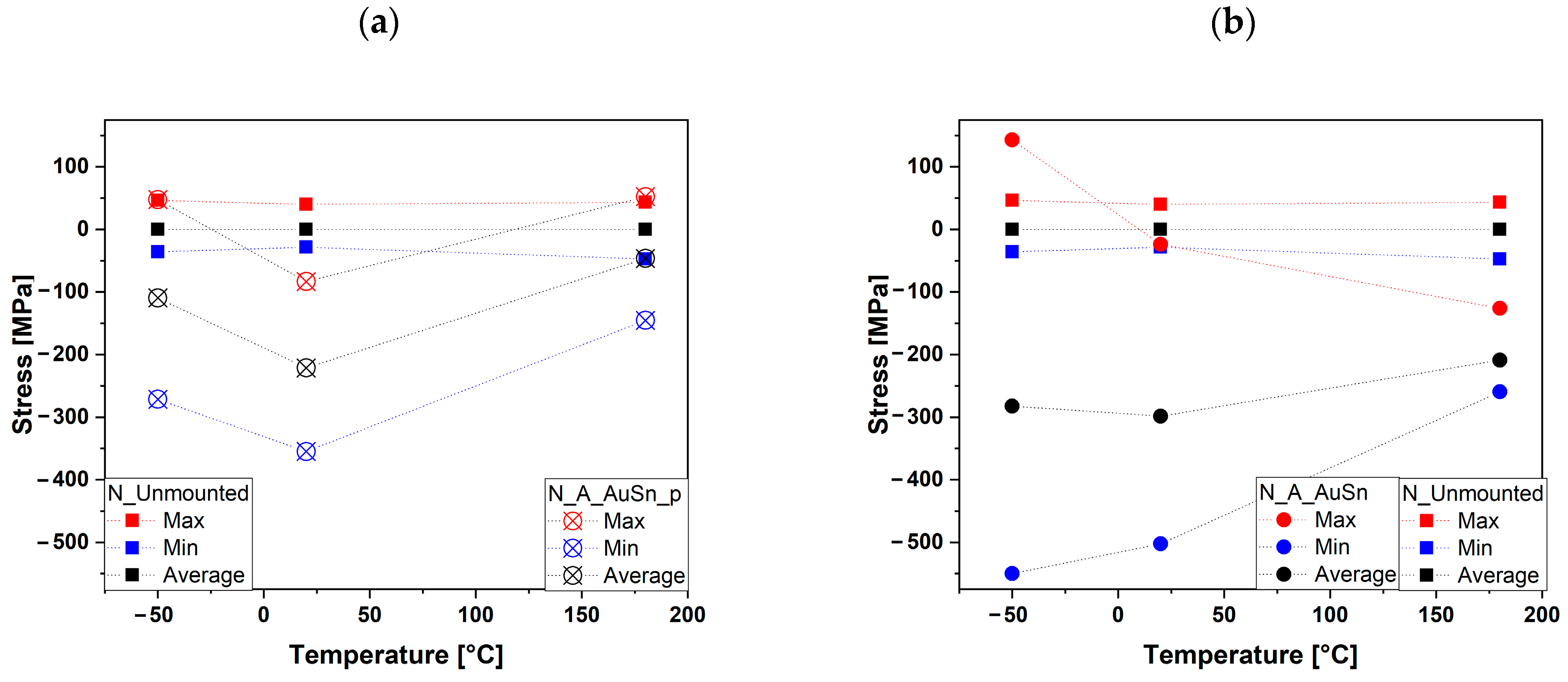
| Temperature [°C] | Maximum Value | Minimum Value | Average Value | Maximum Variation | |
|---|---|---|---|---|---|
| −50 | Raman shift [cm−1] | 863.8 ± 0.1 | 863.5 ± 0.1 | 863.7 ± 0.1 | 0.2 |
| Stress [MPa] | 46 ± 24 | −36 ± 24 | 0 | 82 | |
| 20 | Raman shift [cm−1] | 862.8 ± 0.1 | 862.5 ± 0.1 | 862.7 ± 0.1 | 0.3 |
| Stress [MPa] | 40 ± 24 | −28 ± 24 | 0 | 68 | |
| 180 | Raman shift [cm−1] | 860.0 ± 0.1 | 859.7 ± 0.1 | 859.8 ± 0.1 | 0.3 |
| Stress [MPa] | 43 ± 24 | −47 ± 24 | 0 | 90 |
| Temperature [°C] | Maximum Value | Minimum Value | Average Value | Maximum Variation | |
|---|---|---|---|---|---|
| −50 | Raman shift [cm−1] | 866.1 ± 0.1 | 863.2 ± 0.1 | 864.9 ± 0.1 | 2.9 |
| Stress [MPa] | 142 ± 26 | −550 ± 45 | −282 ± 25 | 692 | |
| 20 | Raman shift [cm−1] | 864.6 ± 0.1 | 862.6 ± 0.1 | 863.9 ± 0.1 | 2 |
| Stress [MPa] | −24 ± 24 | −502 ± 43 | −298 ± 16 | 478 | |
| 180 | Raman shift [cm−1] | 860.9 ± 0.1 | 860.5 ± 0.1 | 860.7 ± 0.1 | 0.5 |
| Stress [MPa] | −126 ± 25 | −259 ± 30 | −208 ± 24 | 133 |
| Temperature [°C] | Maximum Value | Minimum Value | Average Value | Maximum Variation | |
|---|---|---|---|---|---|
| −50 | Raman shift [cm−1] | 864.7 ± 0.1 | 863.6 ± 0.1 | 864.2 ± 0.1 | 1.1 |
| Stress [MPa] | 47 ± 24 | −271 ± 30 | −109 ± 31 | 318 | |
| 20 | Raman shift [cm−1] | 864.1 ± 0.1 | 863.0 ± 0.1 | 863.5 ± 0.1 | 1.1 |
| Stress [MPa] | −83 ± 24 | −355 ± 34 | −221 ± 28 | 272 | |
| 180 | Raman shift [cm−1] | 860.3 ± 0.1 | 859.8 ± 0.1 | 860.0 ± 0.1 | 0.8 |
| Stress [MPa] | 52 ± 24 | −145 ± 26 | −46 ± 18 | 192 |
Disclaimer/Publisher’s Note: The statements, opinions and data contained in all publications are solely those of the individual author(s) and contributor(s) and not of MDPI and/or the editor(s). MDPI and/or the editor(s) disclaim responsibility for any injury to people or property resulting from any ideas, methods, instructions or products referred to in the content. |
© 2024 by the authors. Licensee MDPI, Basel, Switzerland. This article is an open access article distributed under the terms and conditions of the Creative Commons Attribution (CC BY) license (https://creativecommons.org/licenses/by/4.0/).
Share and Cite
Mezzalira, C.; Conti, F.; Pedron, D.; Signorini, R. Raman Investigation on Silicon Nitride Chips after Soldering onto Copper Substrates. Micromachines 2024, 15, 990. https://doi.org/10.3390/mi15080990
Mezzalira C, Conti F, Pedron D, Signorini R. Raman Investigation on Silicon Nitride Chips after Soldering onto Copper Substrates. Micromachines. 2024; 15(8):990. https://doi.org/10.3390/mi15080990
Chicago/Turabian StyleMezzalira, Claudia, Fosca Conti, Danilo Pedron, and Raffaella Signorini. 2024. "Raman Investigation on Silicon Nitride Chips after Soldering onto Copper Substrates" Micromachines 15, no. 8: 990. https://doi.org/10.3390/mi15080990
APA StyleMezzalira, C., Conti, F., Pedron, D., & Signorini, R. (2024). Raman Investigation on Silicon Nitride Chips after Soldering onto Copper Substrates. Micromachines, 15(8), 990. https://doi.org/10.3390/mi15080990