Abstract
In this paper, a novel p-type junctionless field effect transistor (PJLFET) based on a partially depleted silicon-on-insulator (PD-SOI) is proposed and investigated. The novel PJLFET integrates a buried N+-doped layer under the channel to enable the device to be turned off, leading to a special work mechanism and optimized performance. Simulation results show that the proposed PJLFET demonstrates an Ion/Ioff ratio of more than seven orders of magnitude, with Ion reaching up to 2.56 × 10⁻⁴ A/μm, Ioff as low as 3.99 × 10⁻¹² A/μm, and a threshold voltage reduced to −0.43 V, exhibiting excellent electrical characteristics. Furthermore, a new CMOS inverter comprising a proposed PJLFET and a conventional NMOSFET is designed. With the identical geometric dimensions and gate electrode, the pull-up and pull-down driving capabilities of the proposed CMOS are equivalent, showing the potential for application in high-performance chips in the future.
1. Introduction
The scaling of metal oxide field-effect transistors (MOSFETs) to the nanometer regime faces several challenges, and the performance of PMOS becomes one of the key factors limiting the development of CMOS technology [1,2,3]. Since the mobility of holes is approximately half that of electrons, PMOS requires a larger size to compensate for its lower mobility to achieve the same current driving capability with NMOS, which affects the miniaturization of CMOS devices. To improve the mobility of PMOS devices and enhance the performance of CMOS devices, some studies focus on improving PMOS-driven capability by using lower bandgap materials [4,5,6,7]. However, the off-state current could rise simultaneously, leading to high standby power consumption. Moreover, the devices with hetero-materials have also posed a severe challenge to the fabrication process. Other studies try to enhance driving current with silicon-based PMOS by modifying structures [8,9,10,11]. Among them, the junctionless FET (JLFET) is one of the effective ways to improve the performance of PMOS devices.
Junctionless field effect transistors (JLFETs) have the advantages of higher carrier mobility, lower resistance and stronger driving ability [12,13,14,15] due to their special working mechanism. These JLFETs usually have the same doping type in the source, channel, and drain regions, so there is no PN junction along the current flow direction, as shown in Figure 1. Meanwhile, a large difference in work function between the gate electrode and channel is required to achieve volume depletion in the channel, shutting the device down in the off state. With an increasing gate bias voltage, the depletion region under the gate dies away from the bottom of channel to the surface of channel, and the entire channel region becomes neutral finally, allowing carriers to flow from source to drain. Due to the special work mechanism, the movement of charge carriers in the channel is subject to less scattering, enhancing their mobility significantly. Thus, JLFETs are characterized as bulk conductive devices and work in flatband mode or accumulation mode, and the driving ability is much better than that of conventional MOSFETs [16,17].
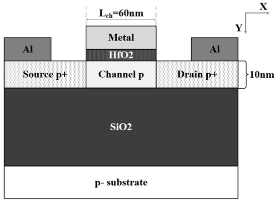
Figure 1.
Cross-section of conventional PJLFET based on FD-SOI substrate.
However, since the semiconductor film is heavily doped in JLFETs, to achieve volume depletion, the gate electrode work function of JLFET has to be adjusted to shut down the device in the off state. For p-type JLFET (p-JLFET), a low work function (≤4.1 eV) is required to achieve volume depletion under the gate in the channel region to completely inhibit majority-carrier current flow from source to drain. The gate electrode with low work function deteriorates the performance of the device: the surface electric field of the device in the off state is high, resulting in a serious gate-induced drain leakage (GIDL) effect which is the main component of the off-state current in JLFET [18,19,20], and a large gate voltage is required for the channel to exit the depletion state, causing a relatively high threshold voltage VTH of p-JLFET. In addition, to realize efficient volume depletion of the channel in p-JLFETs, the silicon film is ultrathin (thickness ≤ 10 nm). The use of ultrathin silicon films, such as fully depleted SOI (FD-SOI), is costly [21]. Moreover, producing ultrathin silicon films with a uniform thickness over the entire wafer is a challenge [22].
Thus, in this paper, a novel p-type JLFET based on partially depleted SOI (PD-SOI) is proposed and studied for the first time. The novel PJLFET integrates a buried N+ doping layer under the channel to turn off the device, reducing the requirements for the gate electrode and the ultrathin silicon film. With the new structure, the proposed PJLFET is supposed to achieve both high on-state current (Ion) and low off-state current (Ioff), keeping VTH relatively low at the same time. The performance of the proposed PJLFET is verified and studied by using a TCAD simulator. Simulation results show that the proposed PJLFET demonstrates an Ion/Ioff ratio of more than 7 decades of magnitude with Ion up to 2.56 × 10⁻⁴ A/μm, Ioff down to 3.99 × 10⁻¹² A/μm, and VTH is −0.43 V. Furthermore, a new CMOS inverter is designed. The new CMOS is composed of a proposed PJLFET and a conventional NMOSFET, and the voltage transfer characteristic (VTC) and output transient characteristic are examined in detail.
2. Device Structure and Simulation Approach
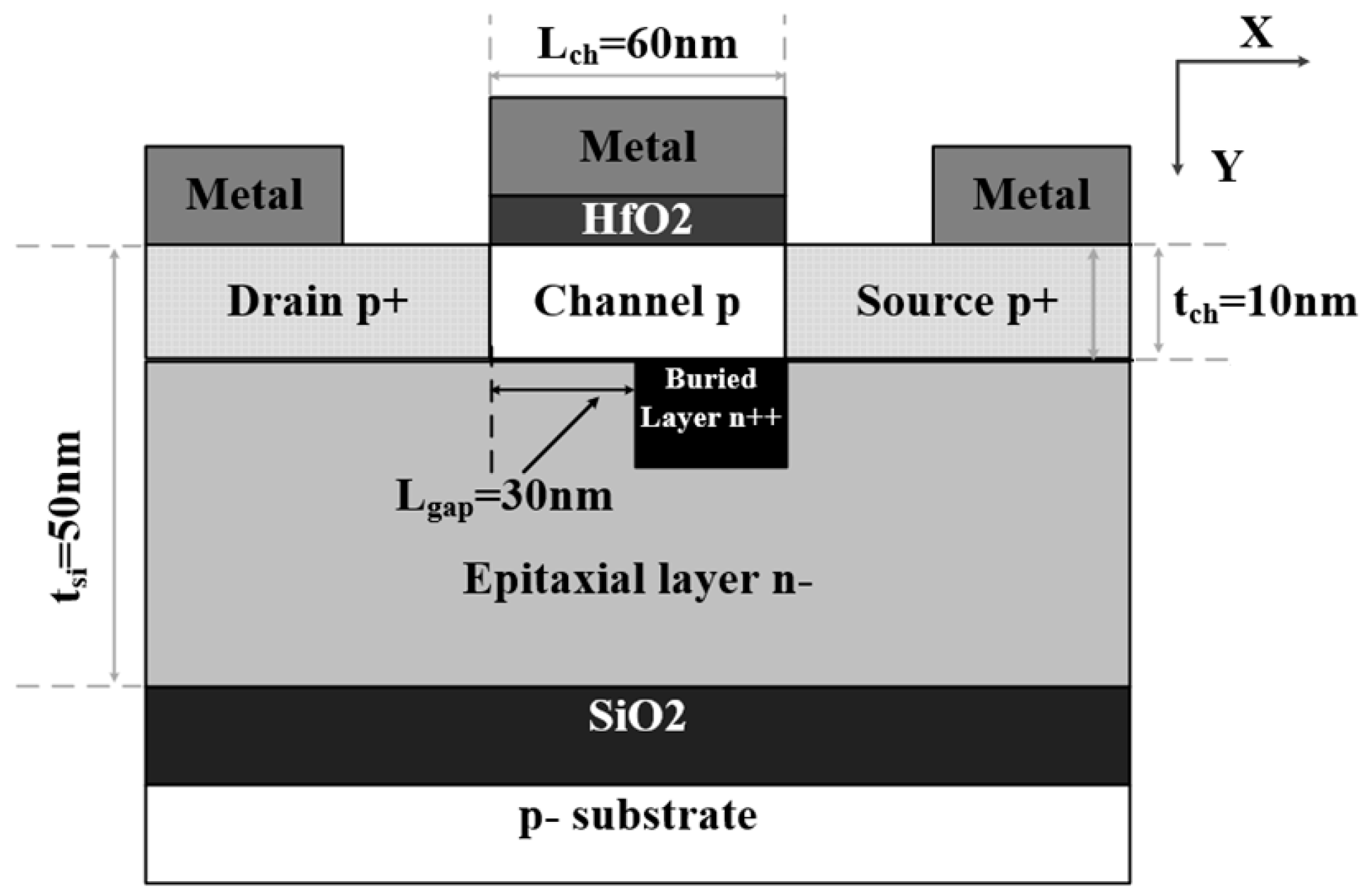
Figure 2 shows the cross-section of the proposed p-type JLFET with a buried N+-doped layer (BNL PJLFET) based on PD-SOI. Different from conventional PJLFETs, the proposed BNL PJLFET has a buried N+ doped layer (BN layer) under the channel, and an electrode with a work function of 4.8 eV is used for the JLFET gate metal. Due to the heavily doped BN layer, a higher point-tunneling probability occurs between the BN layer and drain in the off state. So, the gap (Lgap) between the BN layer and the edge of the gate electrode is introduced to restrict the point tunneling at zero gate bias. In addition, the channel is lightly doped compared with the BN layer to ensure its depletion, and the high k material of HfO2 is used as gate oxide dielectric. The parameters used in our simulation are shown in Table 1.
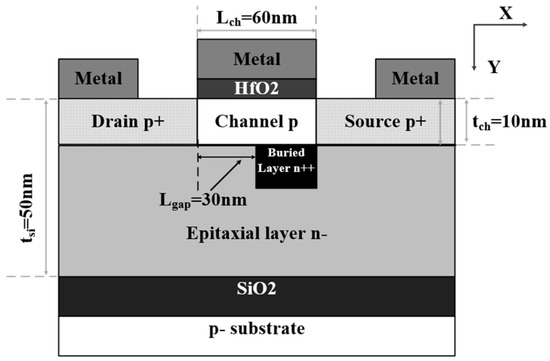
Figure 2.
Cross-section of BNL PJLFET based on PD-SOI substrate.

Table 1.
Simulated device parameters used in this study.
The simulation is carried out using the Sentaurus TCAD simulator. The simulation models used in [23] were implemented in our simulations. The dynamic nonlocal band-to-band tunneling (BTBT) model is used for BTBT current simulation, while the bandgap narrowing effect and Fermi statistical distribution are also taken into account. The involved parameters are carefully calibrated according to [24,25]. Since the effective bandgap directly influences the tunneling current, the bandgap narrowing (BGN) model is also included. The Shockley–Read–Hall (SRH) recombination model is included due to the presence of high-impurity atom concentration in the channel and the Fermi–Dirac statistics are used to calculate the intrinsic carrier concentration. For more accurate current calculations, the field-dependent, doping-dependent mobility degradation model, and drift-diffusion current transport model, are also considered.
3. Operation Principle of BNL PJLFET
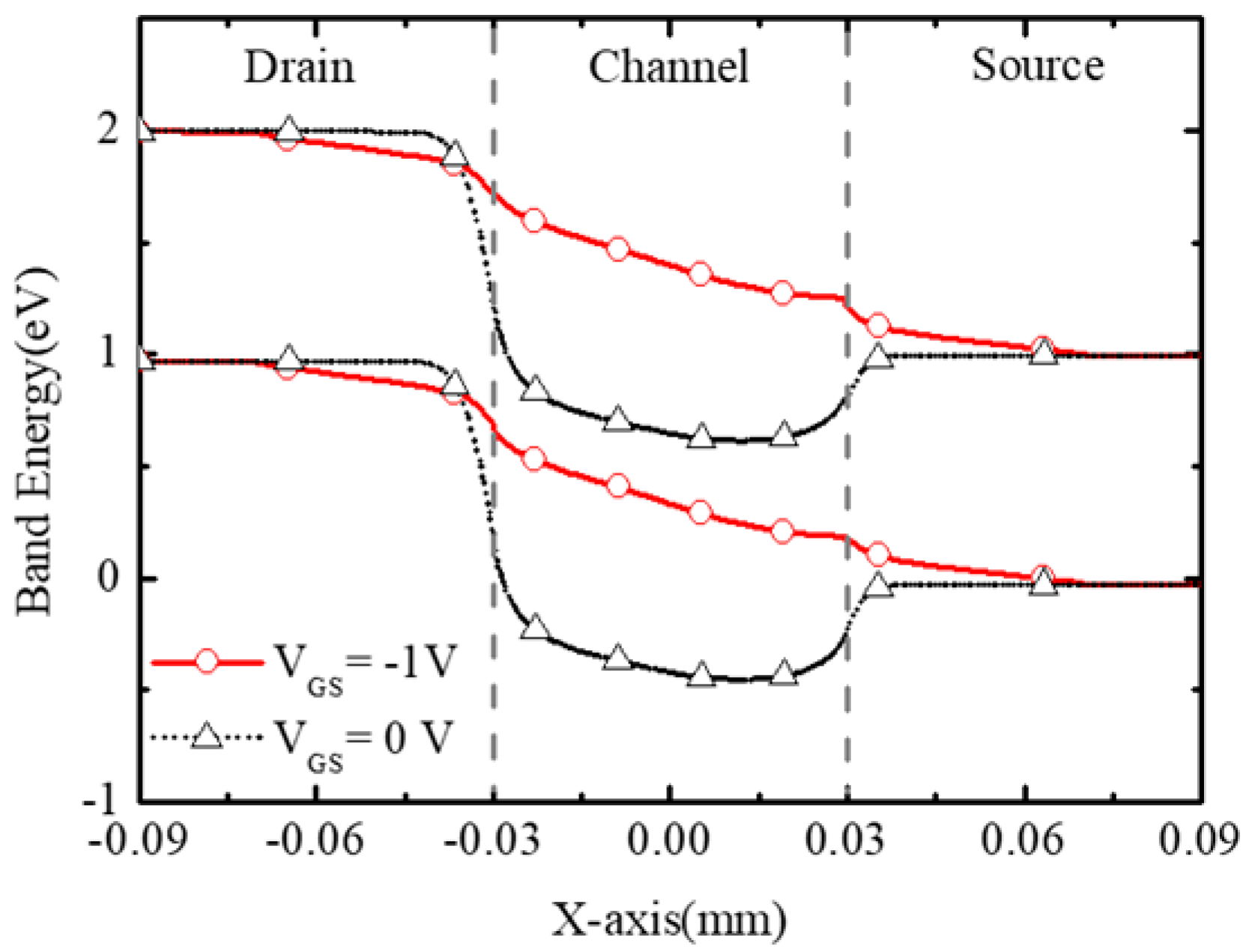
The device operation can be understood from the band diagrams in BNL JLFET illustrated in Figure 3. The simulated band diagrams are along the surface of the channel as shown in Figure 2.
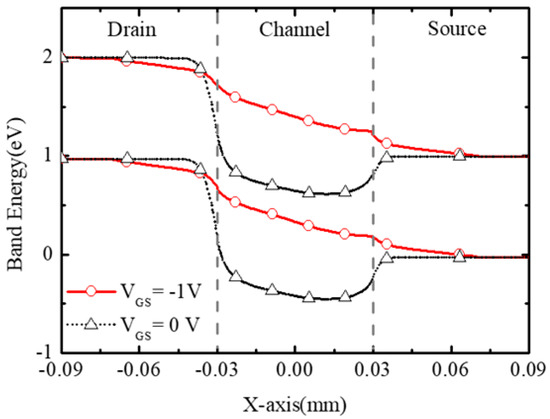
Figure 3.
Band diagrams of BNL PJLFET along the surface of the channel.
At zero gate bias (VGS = 0 V), since the depletion region of the n+/p− junction is mainly distributed on the lightly doped p region, the channel above the BN layer is depleted. So, there is a high barrier (for holes) between the drain and channel, as shown in Figure 3. Thus, the device works in the off state and the current cannot flow from the source to drain.
As the gate bias voltage │VGS│ increases, the hole barrier gradually decreases. Finally, the surface of the channel exits the depletion state and enters a neutral state finally, causing the device to turn on (as shown in Figure 3). Since the depletion state caused by the buried layer is weaker closer to the surface, the holes appear from the surface to the bottom of the channel gradually, being different from the operation of the conventional PJLFETs. At VGS = −1 V, a bulk hole channel is formed, and the holes can flow from source to drain at VDS = −1 V.
4. Results and Discussion
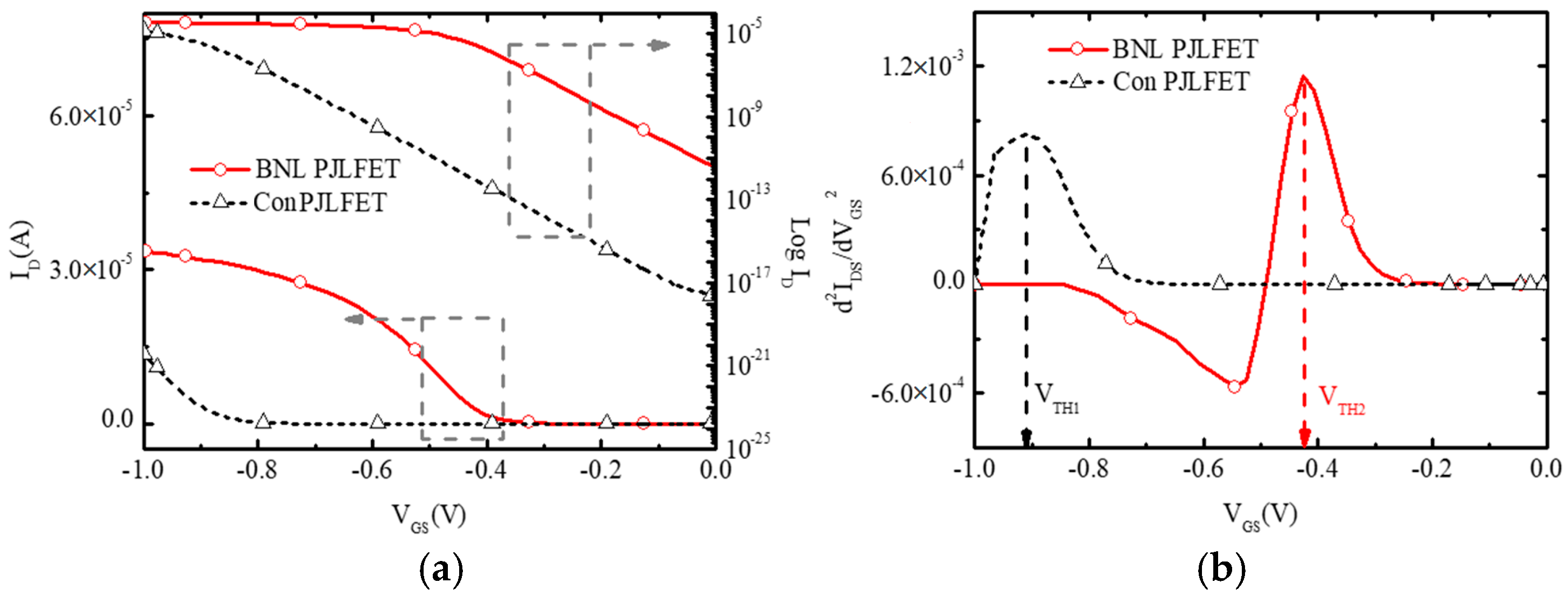
To extract the threshold voltage VTH, the transfer characteristics of the proposed BNL PJLFET and conventional PJLFET at VDS = −0.05 V are obtained, as shown in Figure 4a. To deplete carriers in the channel with a thickness of 10 nm, the conventional PJLFET has a gate electrode with a 4.1 eV work function to shut down the device. A transconductance derivative method is used to extract VTH of JLFETs from transfer curves. Figure 4b calculates the d2IDS/dVGS2 curves as a function of VGS. It can be seen that the maximum d2IDS/dVGS2 values of the proposed BNL PJLFET and conventional PJLFET are obtained at VGS = −0.43 V and VGS = −0.91 V, which indicates VTH of BNL PJLFET is much smaller than that of conventional PJLFET, as a result of the increase in work function of the gate electrode as mentioned above.
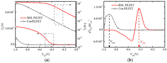
Figure 4.
Extraction of VTH of BNL PJLFET and conventional PJLFET. (a) Transfer characteristics at VDS = −0.05 V (b) d2IDS/dVGS2 curves.
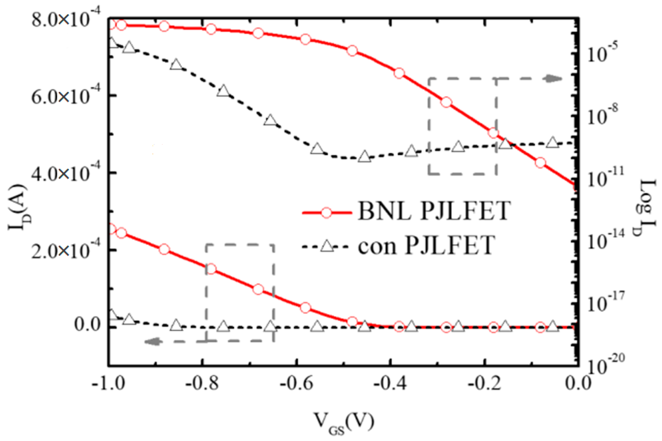
Figure 5 shows the transfer characteristics of conventional PJLFET and the proposed BNL PJLFET at VDS = −1 V. As discussed above, the VTH of BNL PJLFET is lower than that of conventional JLFET. Thus, the on-state current Ion of BNL PJLFET extracted at VGS = −1 V obtains a value of 2.56 × 10⁻⁴ A/μm, which is larger than the value of 3.17 × 10⁻⁵ A/μm extracted in conventional PJLFET. Meanwhile, off-state current Ioff of BNL PJLFET at VGS = 0 V is 3.99 × 10⁻¹² A/μm, which is two orders of magnitude lower than that in conventional PJLFET, leading to a high Ion/Ioff ratio of 6.42 × 10⁷.
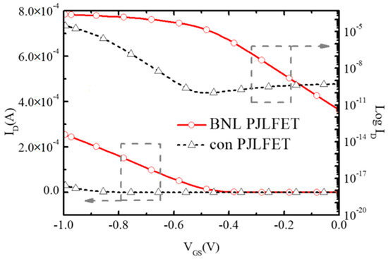
Figure 5.
Transfer characteristic of the BNL PJLFET and the conventional PJLFET at VDS = −1 V.
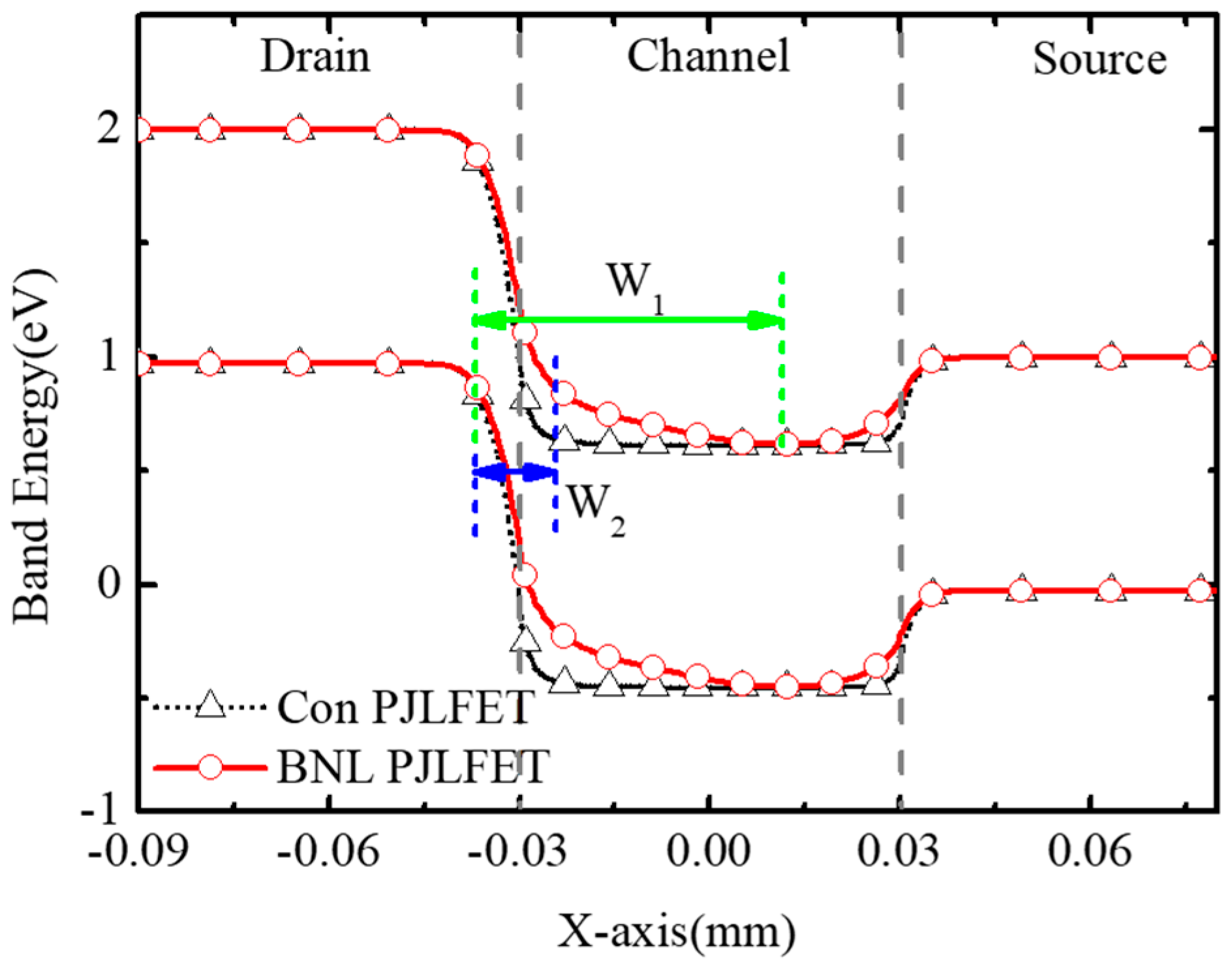
Figure 6 shows the evidence of the GIDL suppression in the off state (VDS = −1 V, VGS = 0 V) of the BNL PJLFET. W1 and W2 represent the tunneling width in BNL JLFET and conventional JLFET, respectively. Due to the optimization of the work function of the gate electrode and the introduction of the gap between the BNL and the drain, the tunneling width W1 at the drain–channel interface of BNL JLFET is significantly larger than that of conventional JLFETs. An enlarged tunneling width leads to a reduction in the tunneling probability of electrons from the drain region to the channel region, as pointed out in the literature [26], and decreases the off-state current Ioff in the BNL PJLFET.
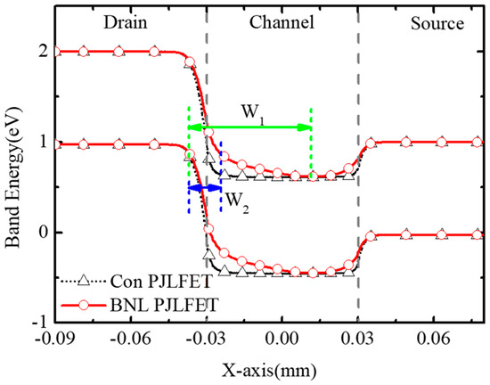
Figure 6.
Tunneling width at the channel surface of the BNL PJLFET and the conventional PJLFET at VGS = 0 V, VDS = −1 V.
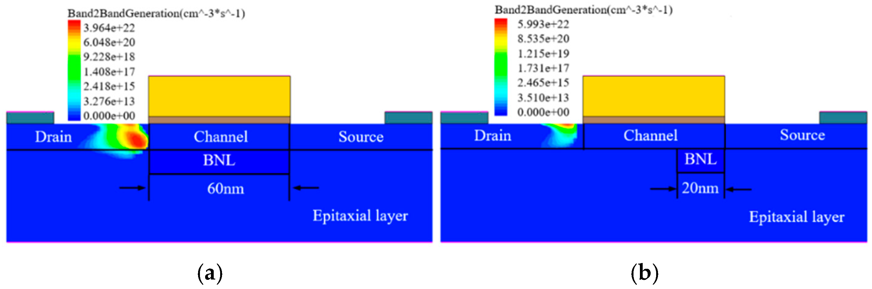
As discussed in Section 2, there is a significant band to band tunneling between the drain region and the BN layer. Figure 7 shows the BTBT probability with LBN = 60 nm and 20 nm, respectively. It can be seen that a significant BTBT occurs at the drain–BN junction at LBN = 60 nm. To suppress the BTBT effect between the drain and BN layer, the gap between the drain and BNL is introduced. With the decrease of LBN, the highest BTBT probability point moves from the interior of the device to the surface at the interface of the drain and channel, eliminating the influence of bulk tunneling on the off-state current.
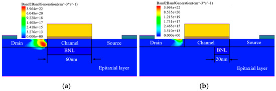
Figure 7.
Band to band tunneling probability distribution at the surface of BNL PJLFET with (a) LBN = 20 nm and (b) LBN = 60 nm when VGS = 0 V, VDS = −1 V.
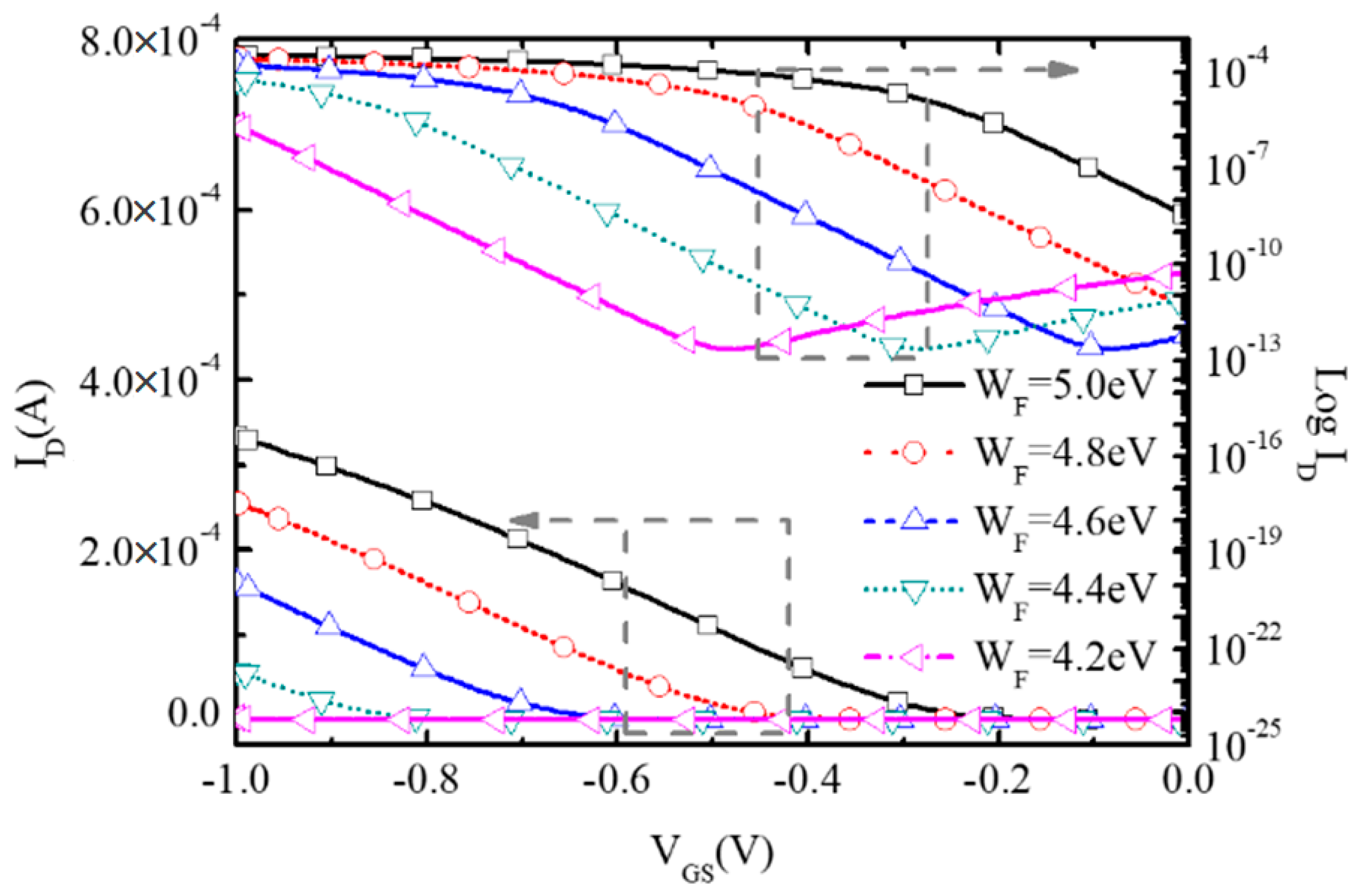
Figure 8 shows the influence of the work function (WF) of the gate electrode on the transfer characteristics of BNL JLFET. With the reduction in WF from 5.0 eV to 4.2 eV, the GIDL effect becomes more and more significant, resulting in the increase of Ioff from 8.51 × 10⁻¹² A/μm to 3.04 × 10⁻⁹ A/μm.

Figure 8.
Transfer characteristic of the proposed BNL PJLFET for different work function at VDS = −1 V.
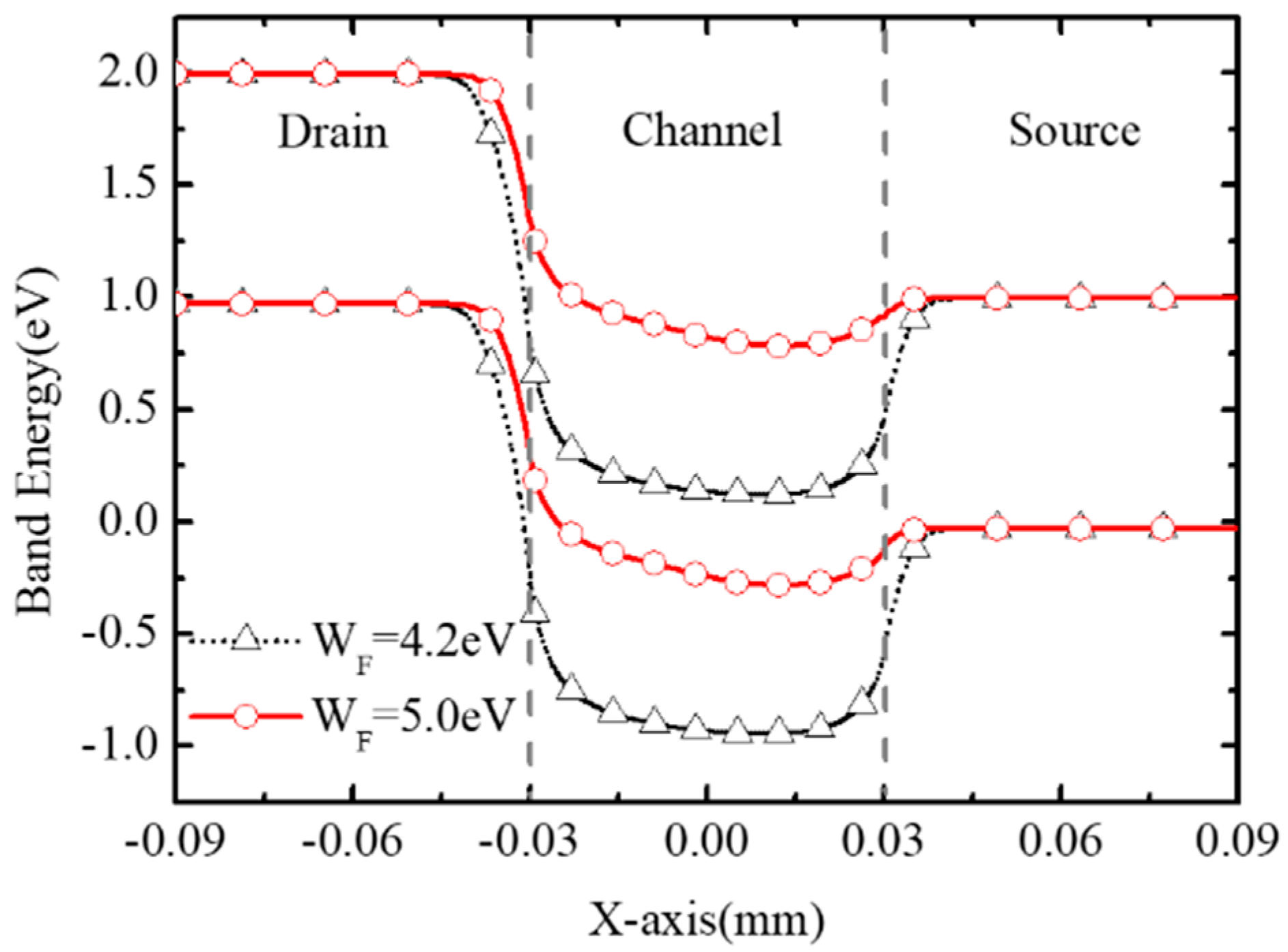
Figure 9 shows the band diagrams of BNL PJLFET for WF = 5.0 eV and 4.2 eV, respectively. It can be seen that the BTBT width at the drain–channel interface with WF = 4.2 eV is narrower than that of the device with WF = 5.0 eV, resulting in the enhancement of band to band tunneling from the drain to channel. Thus, the GIDL effect is enhanced and Ioff increases. Moreover, since the depletion degree in the channel improves as WF changes from 5.0 eV to 4.2 eV, the threshold voltage also increases, resulting in the reduction in on-state current Ion.

Figure 9.
Band diagrams along the surface of the channel with WF = 4.2 eV and 5.0 eV when VGS = 0 V, VDS = −1 V.
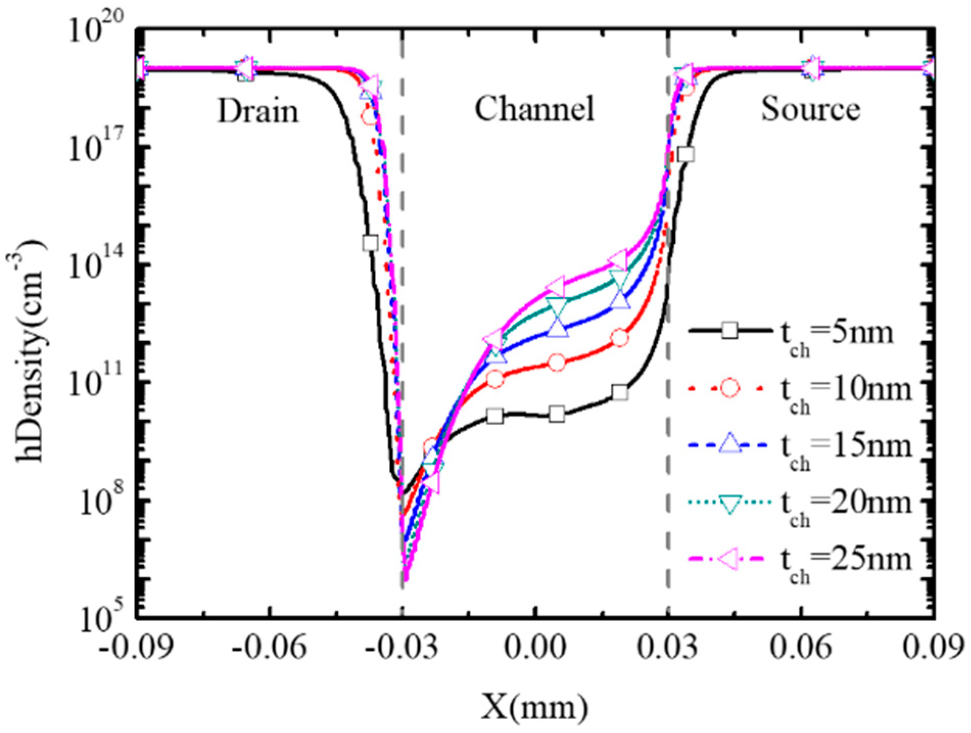
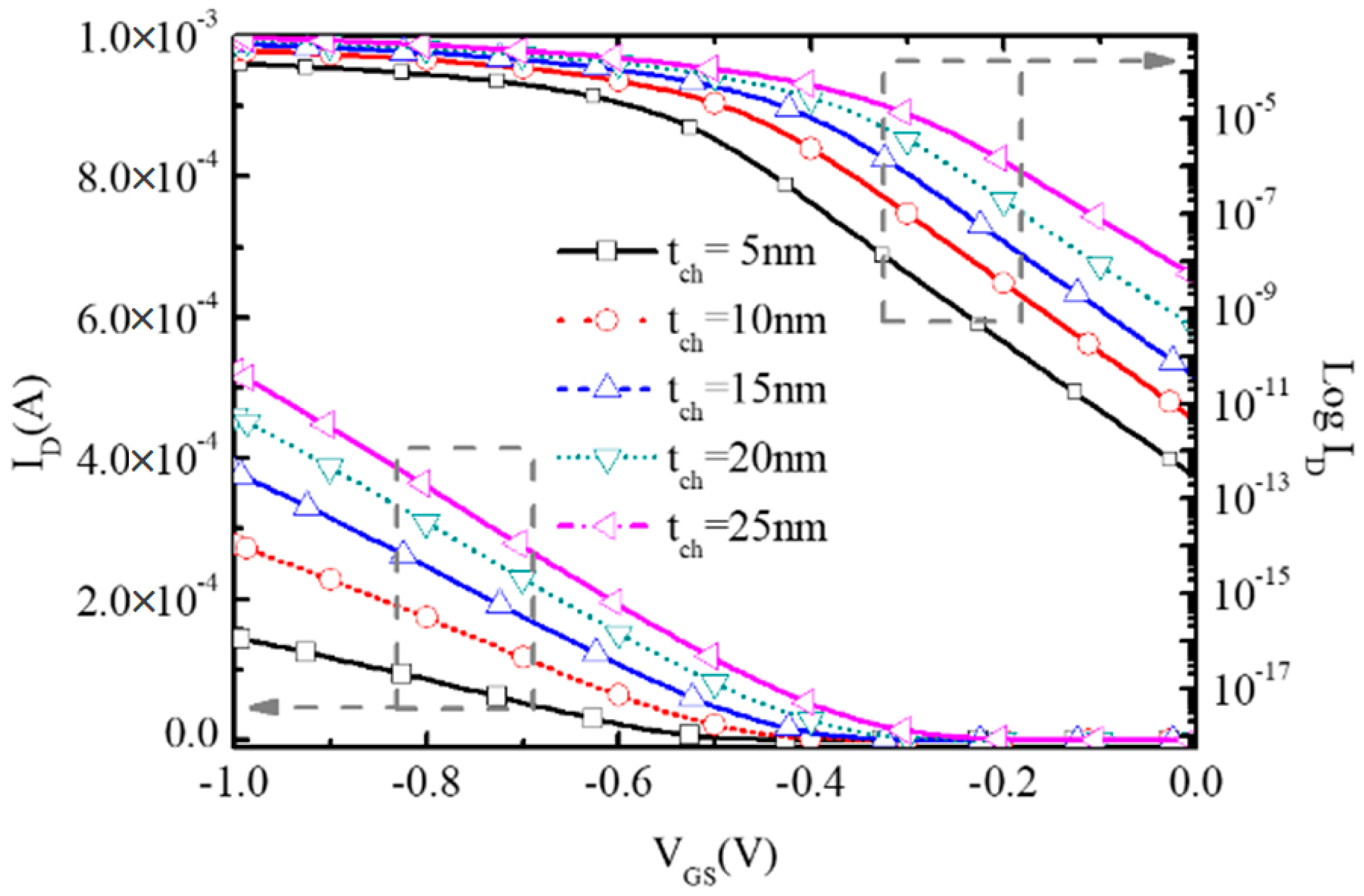
To study the impact of channel thickness tch on the performance of BNL PJLFET, Figure 10 examines the surface hole density with tch changing from 5 nm to 25 nm at VGS = 0 V, VDS = −1 V. Since the channel is depleted by the buried n+/p− junction, a large tch means the reduction in depletion degree at the channel surface. So, at an off state, the surface hole density at tch = 25 nm is higher compared with that at tch = 5 nm, resulting in the increment of off-state current Ioff from 2.85 × 10⁻¹³ A/μm to 4.89 × 10⁻⁹ A/μm, as shown in Figure 11.
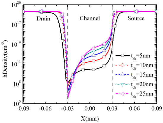
Figure 10.
Surface hole density of BNL pJLFET for different tch at VGS = 0 V, VDS = −1 V.
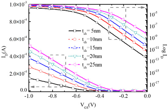
Figure 11.
Transfer characteristic of the proposed BNL PJLFET for different tch at VDS = −1 V.
Owing to the reduction in surface depletion degree, the absolute value of threshold voltage VTH decreases with the increase in the channel thickness as shown in Figure 12. So, the on-state current Ion at VGS = −1 V, VDS = −1 V increases to 5.23 × 10⁻⁴ A/μm at tch = 25 nm, almost three times larger than 1.47 × 10⁻⁴ A/μm at tch = 5 nm shown in Figure 11. However, as the influence of the increment of the channel thickness on off-state current Ioff is more apparent, it can be seen that the subthreshold swing SS deteriorates with the enlargement of the channel thickness in Figure 12.
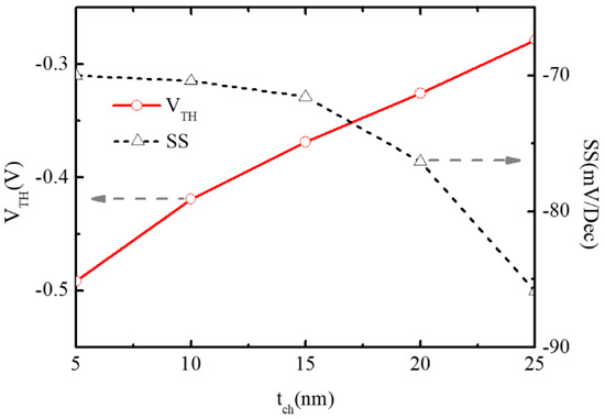
Figure 12.
Variations of VTH and SS of BNL PJLFET with tch changing from 5 nm to 25 nm.
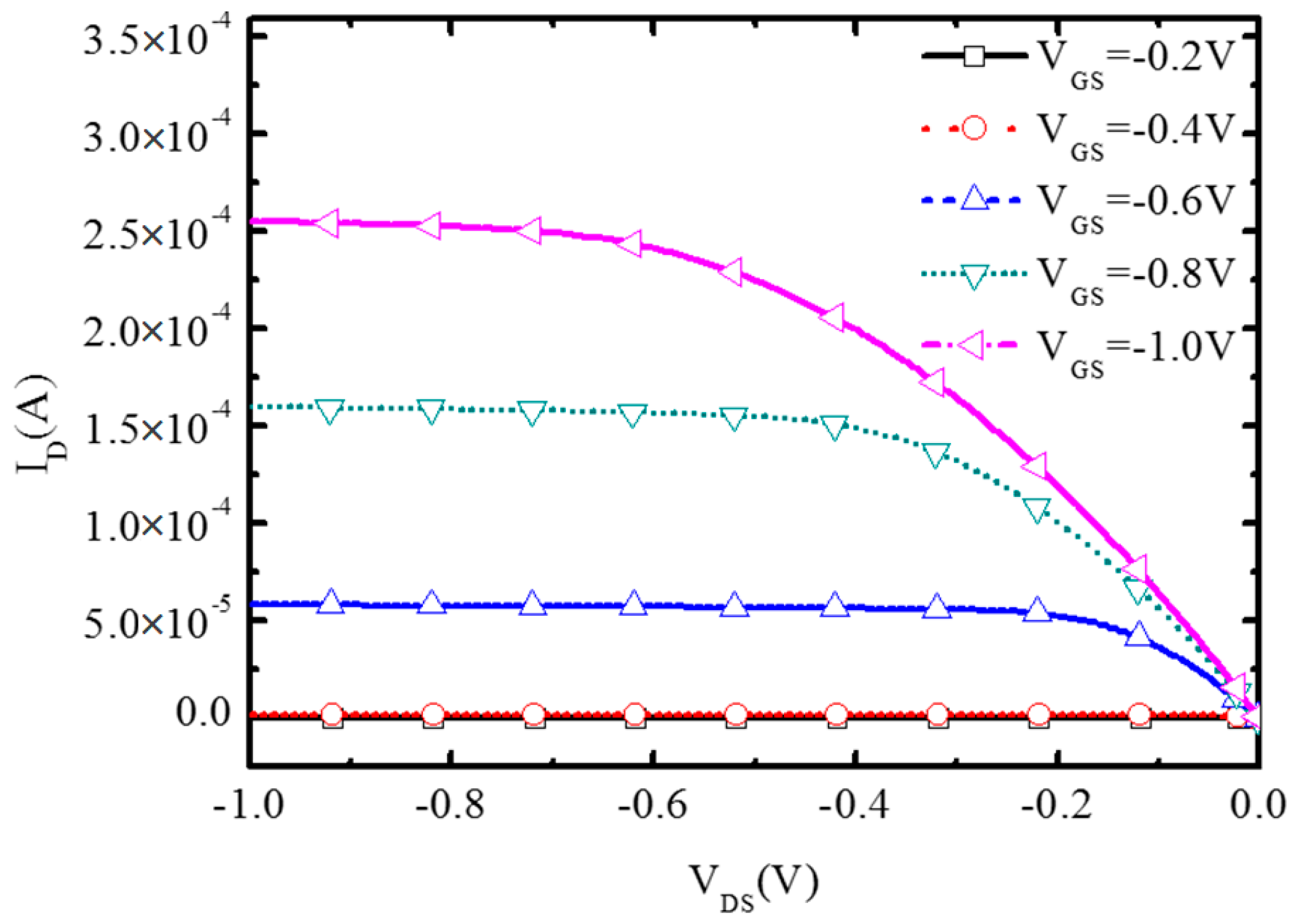
Figure 13 shows the output characteristics of the BNL PJLFET with different gate voltages. The drain current IDS at VGS = −0.2 V, −0.4 V, −0.6 V, −0.8 V, and −1 V increases firstly and then reaches saturation at high drain voltages, showing good conduction characteristics.
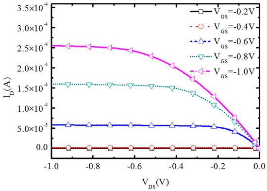
Figure 13.
BNL PJLFET output characteristic curves.
5. Investigation
The investigation of the BNL PJLFET in the CMOS inverter is examined in this section. As shown in Figure 14, the new CMOS inverter consists of a BNL PJLFET as the pull-up device and a conventional NMOS as the pull-down device, where the BNL PJLFET operates in the accumulation region and the conventional NMOS operates in the inversion region. This is completely different from the conventional CMOS devices based on the inversion model. Cout is the load capacitance with the value of 1 × 10⁻¹⁴ F. The parameters of proposed CMOS used in the simulation are shown in Table 2. Moreover, the geometric dimensions of PJLFET and NMOSFET are identical in the new CMOS inverter, and the same metal electrode is used for both devices.
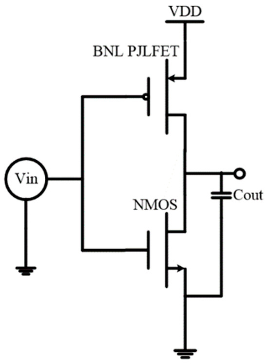
Figure 14.
Inverter circuit in Sentaurus TCAD.
Table 2.
Device parameters used in these CMOS inverters.
Figure 15 shows the VTC (Voltage Transfer Characteristic) curve of the inverter through simulation. It can be seen that the threshold conversion voltage VM of this new inverter is almost at the middle voltage of VIN, showing a good transfer characteristic of the CMOS inverter. This is mainly attributed to the symmetrical performance of conventional NMOS and BNL PJLFET as shown in Figure 16. Figure 16 shows the transfer characteristic curves of BNL PJLFET and conventional NMOS at VDS = 1 V, respectively. The curves of conventional NMOS and BNL PJLFET are almost symmetrical. The extracted threshold voltages of these two devices are -0.45 V and 0.47 V, respectively, showing the evidence for the symmetrical performance of PJLFET and conventional NMOSFET.
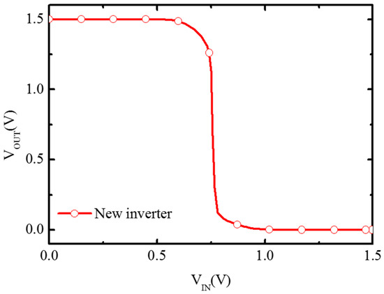
Figure 15.
VTC curve of new inverter.
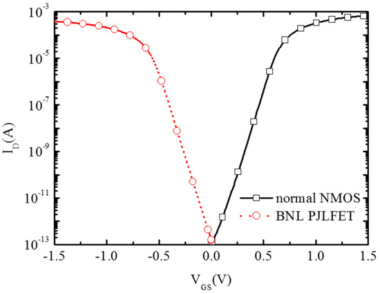
Figure 16.
Transfer characteristic curves of the devices in the inverter.
6. Conclusions
A novel p-type JLFET based on PD-SOI with a buried N+-doped layer under the channel (BNL PJLFET) is proposed in this paper. By introducing a heavily doped N+ buried layer, the device is shut down by the buried p/n junction. Using Sentaurus TCAD tools, the simulation results indicate that BNL PJLFET could effectively suppress the GIDL effect and reduce the threshold voltage, resulting in the improvement of on-state current and on/off current ratio. Furthermore, a new type of CMOS inverter with the BNL PJLFET as a pull-up device was proposed and examined; simulation results show the evidence of performance enhancement of the new CMOS inverter.
Author Contributions
Validation, W.Y.; Investigation, B.W., Z.T. and Y.S.; Writing – review & editing, L.L.; Supervision, B.W.; Funding acquisition, L.W. All authors have read and agreed to the published version of the manuscript.
Funding
This work was supported by the National Natural Science Foundation of China (Grant. No. 61704130) and the Science and Technology on Analog Integrated Circuit Laboratory (Grant No. JCKY2019210C029).
Data Availability Statement
The original contributions presented in the study are included in the article, further inquiries can be directed to the corresponding author.
Conflicts of Interest
The authors declare no conflict of interest.
References
- Ghosh, B.; Bal, P.; Mondal, P. A junctionless tunnel field effect transistor with low subthreshold slope. J. Comput. Electron. 2013, 12, 428–436. [Google Scholar] [CrossRef]
- Lee, C.W.; Ferain, I.; Kranti, A.; Akhavan, N.D.; Razavi, P.; Yan, R.; Yu, R.; O’Neill, B.; Blake, A.; White, M.; et al. Short-channel junctionless nanowire transistors. In Proceedings of the 2010 International Conference on Solid Sate Devices and Materials (SSDM2010), Tokyo, Japan, 22–24 September 2010; pp. 1044–1045. [Google Scholar]
- Boucart, K.; Ionescu, A.M. Double-gate tunnel FET with high-κ gate dielectric. IEEE Trans. Electron Devices 2007, 54, 1725–1733. [Google Scholar] [CrossRef]
- Tang, X.; Hua, T.; Liu, Y.; Han, Z. Heterogeneous CMOS Integration of InGaAs-OI nMOSFETs and Ge pMOSFETs Based on Dual-Gate Oxide Technique. Micromachines 2022, 13, 1806. [Google Scholar] [CrossRef]
- Arimura, H.; Cott, D.; Boccardi, G.; Loo, R.; Wostyn, K.; Brus, S.; Capogreco, E.; Opdebeeck, A.; Witters, L.; Conard, T.; et al. A record GmSAT/SSSAT and PBTI reliability in Si-passivated Ge nFinFETs by improved gate stack surface preparation. In Proceedings of the 2019 Symposium on VLSI Technology, Kyoto, Japan, 9–14 June 2019; pp. T92–T93. [Google Scholar]
- Capogreco, E.; Arimura, H.; Witters, L.; Vohra, A.; Porret, C.; Loo, R.; De Keersgieter, A.; Dupuy, E.; Marinov, D.; Hikavyy, A.; et al. High performance strained Germanium Gate All Around p-channel devices with excellent electrostatic control for sub-Jtlnm LG. In Proceedings of the 2019 Symposium on VLSI Technology, Kyoto, Japan, 9–14 June 2019; pp. T94–T95. [Google Scholar]
- Cai, X.; Vardi, A.; Grajal, J.; Alamo, J.A.D. Reassessing InGaAs for logic: Mobility extraction in sub-10nm fin-width FinFETs. In Proceedings of the 2019 Symposium on VLSI Technology, Kyoto, Japan, 9–14 June 2019; pp. T246–T247. [Google Scholar]
- Ahn, T.J.; Yu, Y.S. Circuit Simulation Considering Electrical Coupling in Monolithic 3D Logics with Junctionless FETs. Micromachines 2020, 11, 887. [Google Scholar] [CrossRef] [PubMed]
- Lee, G.J.; Yu, Y.S. An Investigation of the Effect of the Work-Function Variation of a Monolithic 3D Inverter Stacked with MOSFETs. Micromachines 2022, 13, 1524. [Google Scholar] [CrossRef] [PubMed]
- Li, Z.-H.; Li, R.-L.; Jiang, Y.-L.; Zhang, Y.-W.; Cao, Y.-F.; Wang, X.-J. Performance Improvement by Blanket Boron Implant in the Sigma-Shaped Trench Before the Embedded SiGe Source/Drain Formation for 28-nm PMOSFET. IEEE Electron Device Lett. 2020, 41, 796–799. [Google Scholar] [CrossRef]
- Qureshi, S.; Mehrotra, S. Potential Well Based FDSOI MOS-FET: A Novel Planar Device for 10 nm Gate Length. In Proceedings of the 2019 IEEE SOI-3D-Subthreshold Microelectronics Technology Unified Conference (S3S), San Jose, CA, USA, 14–17 October 2019; pp. 1–3. [Google Scholar]
- Sreenivasulu, V.B.; Prasad, M.; Deepthi, E.; Kumar, A.S. Analysis of Novel Core-Shell Junctionless Nnosheet FET for CMOS Logic Applications. IEEE Access 2024, 12, 144479–144488. [Google Scholar] [CrossRef]
- Gu, J.; Zhang, Q.; Wu, Z.; Yao, J.; Zhang, Z.; Zhu, X.; Wang, G.; Li, J.; Zhang, Y.; Cai, Y.; et al. Cryogenic Transport Characteristics of P-Type Gate-All-Around Silicon Nanowire MOSFETs. Nanomaterials 2021, 11, 309. [Google Scholar] [CrossRef] [PubMed]
- Jhan, Y.-R.; Thirunavukkarasu, V.; Wang, C.-P.; Wu, Y.-C. Performance evaluation of Silicon and Germanium ultrathin body (1 nm) junctionless field-effect transistor with ultrashort gate lengh (1 nm and 3 nm). IEEE Electron Device Lett. 2015, 36, 654–656. [Google Scholar] [CrossRef]
- Chaudhary, S.; Dewan, B.; Singh, D.; Yadav, M. Impact of Temperature Sensitivity on Dead Channel Junctionless FET for Linearity and High Frequency. Semicond. Sci. Technol. 2024, 39, 125012. [Google Scholar] [CrossRef]
- Parmar, J.S.; Sahu, C. CMOS-Compatible Ex-Situ Incorporated Junctionless Enhancement-Mode Thin Polysilicon Film FET pH Sensor. IEEE Trans. Device Mater. Reliab. 2021, 21, 2–8. [Google Scholar] [CrossRef]
- Sreenivasulu, V.B.; Kumar, N.A.; Lokesh, V.; Ajayan, J.; Uma, M.; Vijayvargiya, V. Design of Resistive Load Inverter and Common Source Amplifier Circuits using Symmetric and Asymmetric Nanowire FETs. J. Electron. Meter. 2023, 52, 7268–7279. [Google Scholar] [CrossRef]
- Ye, H.Y.; Chung, C.C.; Liu, C.W. Mobility Calculation of Ge Nanowire Junctionless and Inversion-Mode Nanowire NFETs with Size and Shape Dependence. IEEE Trans. Electron Devices 2018, 65, 5259–5300. [Google Scholar] [CrossRef]
- Shubham, S.; Mamidala, J.K. Insight into Lateral Band-to-Band-Tunneling in Nanowire Junctionless FETs. IEEE Trans. Electron Devices 2016, 63, 4138–4142. [Google Scholar]
- Shubham, S.; Mamidala, J.K. Physical Insights Into the Nature of Gate-Induced Drain Leakage in Ultrashort Channel Nanowire FETs. IEEE Trans. Electron Devices 2017, 64, 2604–2610. [Google Scholar]
- Jung, S.G.; Yu, H.Y. Impact of Random Dopant Fluctuation on n-Type Ge Junctionless FinFETs with Met-al-Interlayer-Semiconductor Source/Drain Contact Structure. IEEE J. Electron Devices Soc. 2019, 7, 1119–1124. [Google Scholar] [CrossRef]
- Jung, S.-G.; Kim, S.-H.; Kim, G.-S.; Yu, H.-Y. Effects of metal-interlayer-semiconductor source/drain contact structure on n-type germanium junctionless FinFETs. IEEE Trans. Electron Devices 2018, 65, 3136–3141. [Google Scholar] [CrossRef]
- Sahay, S.; Kumar, M.J. Junctionless Field-Effect Transistors; Wiley-IEEE Press: Hoboken, NJ, USA, 2019. [Google Scholar]
- Choi, W.Y.; Park, B.; Lee, J.D.; Liu, T.K. Tunneling Field-Effect Transistors (TFETs) with Subthreshold Swing (SS) Less Than 60mV/dec. IEEE Electron Device Lett. 2007, 28, 743–745. [Google Scholar] [CrossRef]
- Mamidala, J.K.; Vishnoi, R.; Pandey, P. Simulation of TFETs. In Tunnel Field-Effect Transistors (TFET): Modelling and Simulation; Wiley: Hoboken, NJ, USA, 2017; pp. 181–193. [Google Scholar]
- Liu, X.Y.; Hu, H.Y.; Wang, B.; Wang, M.; Han, G.Q.; Cui, S.M.; Zhang, H.M. Study of novel junctionless Ge n-Tunneling Field-Effect Transistors with lightly doped drain (LDD) region. Superlattices Microstruct. 2017, 102, 7–16. [Google Scholar] [CrossRef]


Disclaimer/Publisher’s Note: The statements, opinions and data contained in all publications are solely those of the individual author(s) and contributor(s) and not of MDPI and/or the editor(s). MDPI and/or the editor(s) disclaim responsibility for any injury to people or property resulting from any ideas, methods, instructions or products referred to in the content. |
© 2025 by the authors. Licensee MDPI, Basel, Switzerland. This article is an open access article distributed under the terms and conditions of the Creative Commons Attribution (CC BY) license (https://creativecommons.org/licenses/by/4.0/).