
W-Band Low-Noise Amplifier with Improved Stability Using Dual RC Traps in Bias Networks on a 0.1 μm GaAs pHEMT Process


Abstract
:1. Introduction
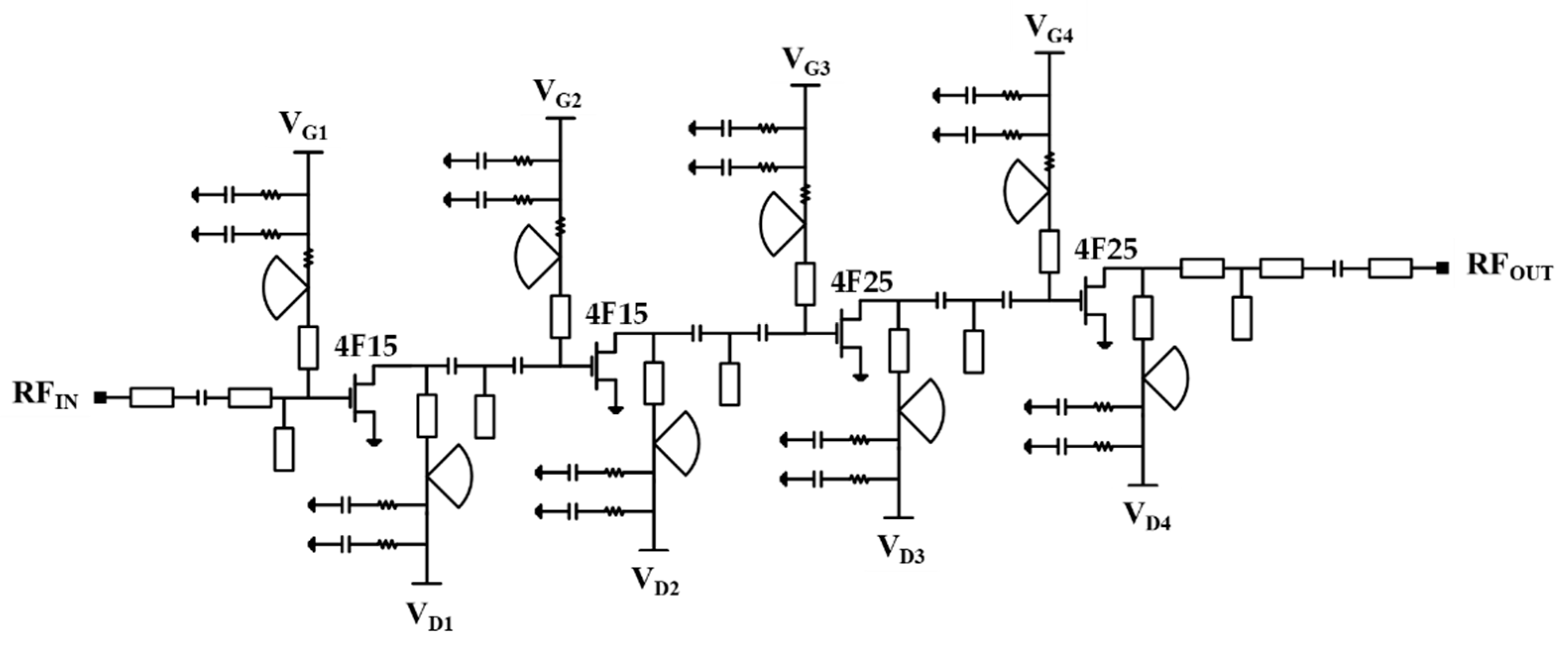
2. Circuit Design
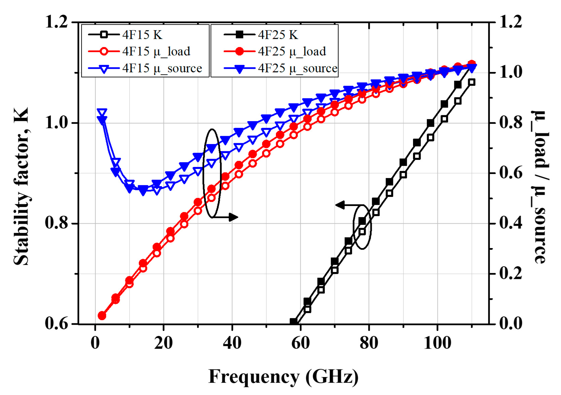
2.1. Device Selection
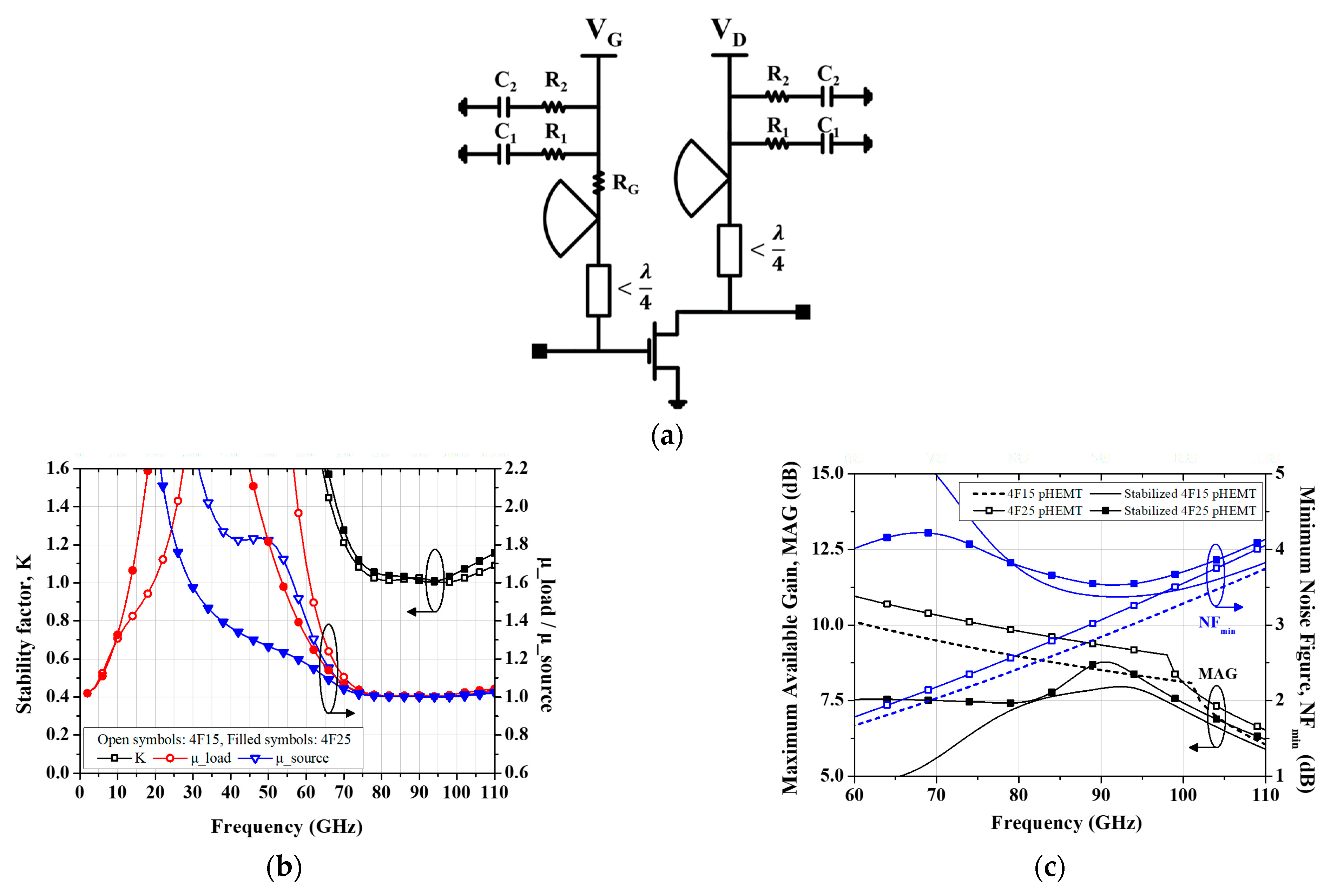
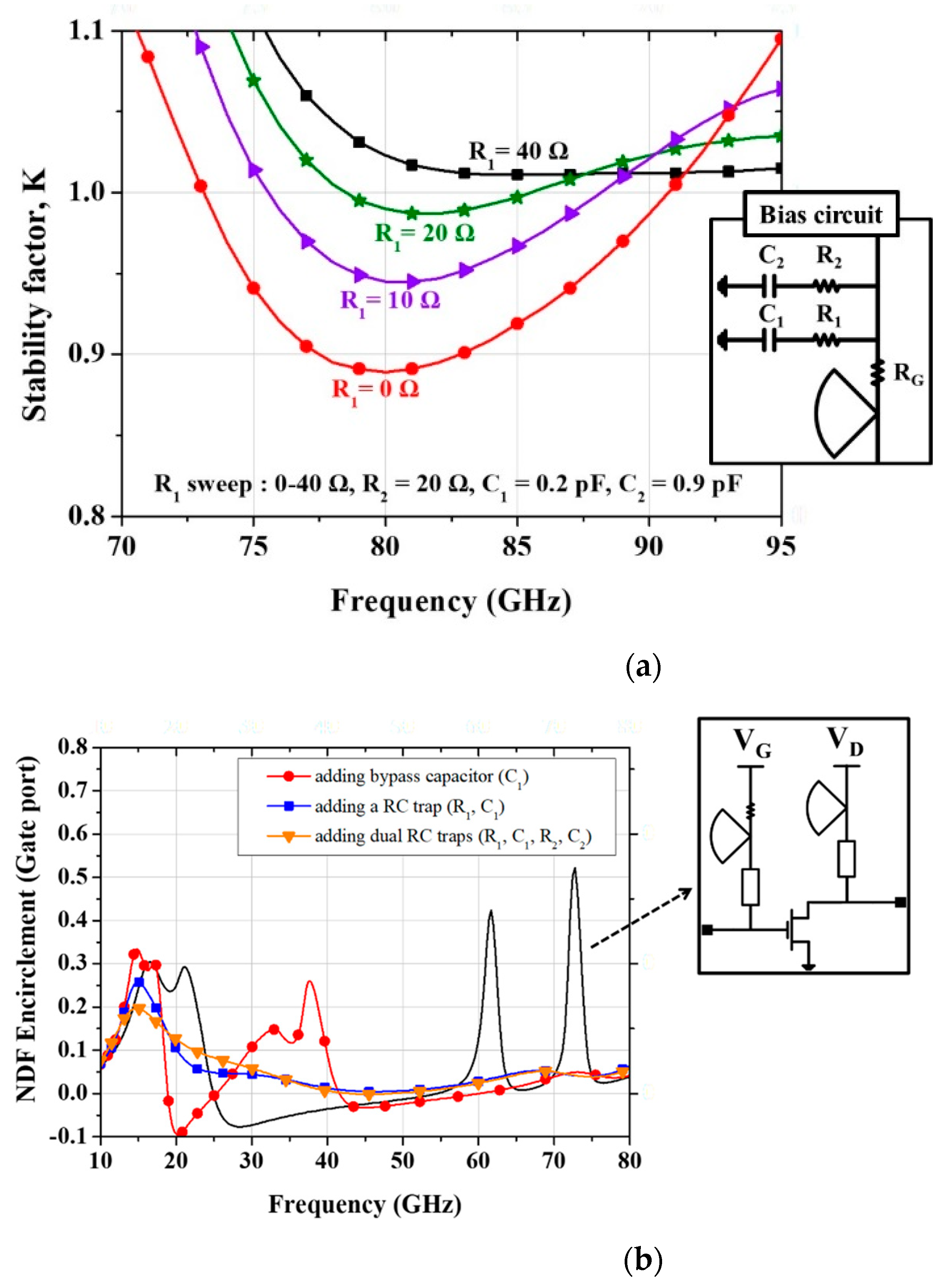
2.2. Stabilization with Dual RC Traps
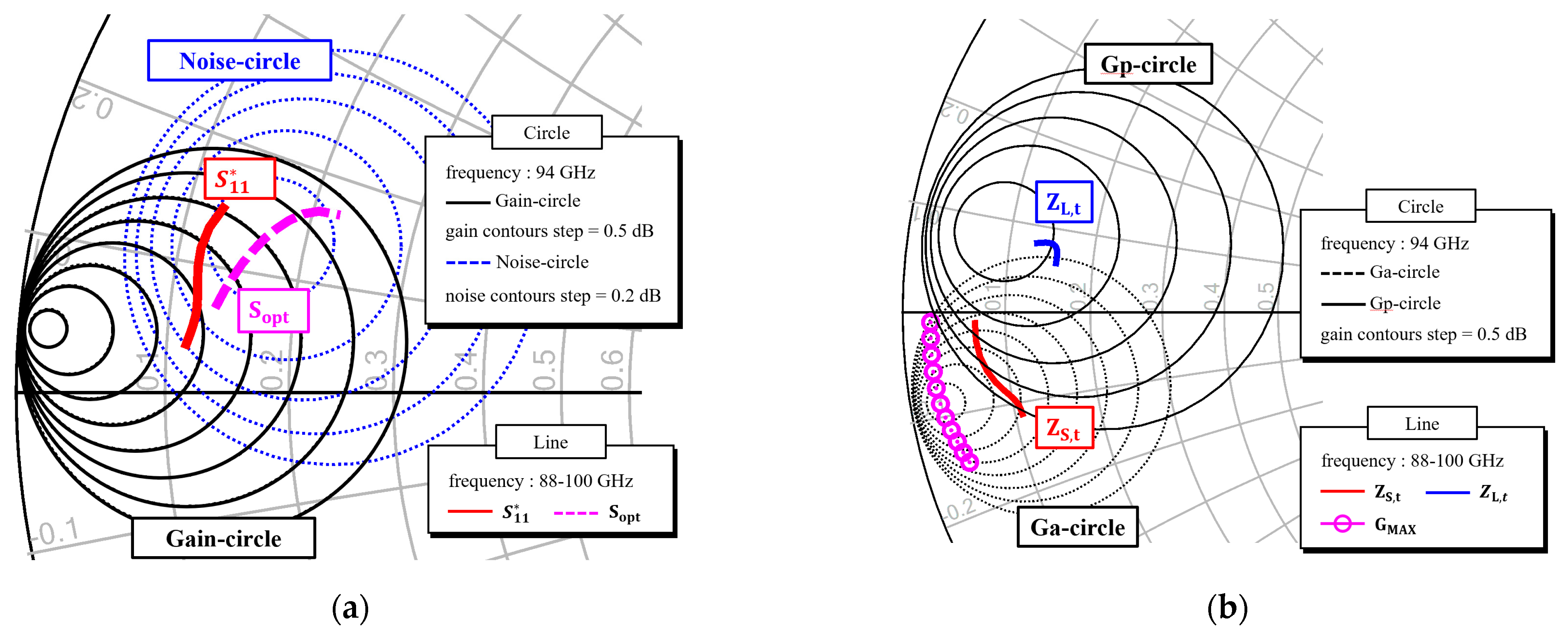
2.3. Circuit Design and Stability Evaluation
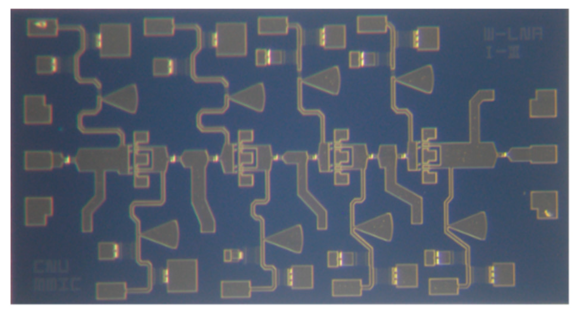
3. Measurement
4. Conclusions
Author Contributions
Funding
Data Availability Statement
Conflicts of Interest
References
- Kim, B.J.; Tran, A.; Schellenberg, J. Full W-band Power Amplifier/Combiner Utilizing GaAs Technology. In Proceedings of the 2012 IEEE/MTT-S International Microwave Symposium Digest, Montreal, QC, Canada, 17–22 June 2012. [Google Scholar]
- Hong, S.E.; Kim, I.E.; Bang, S.C. Trends of Technology Developments for mm-Wave based 5G Mobile Communications. Electron. Telecommun. Trends 2013, 28, 107–117. [Google Scholar]
- Jang, S.H.; Kong, S.W.; Lee, H.D.; Park, J.H.; Kim, K.S.; Lee, K.C. Millimeter and Terahertz Wave Circuit and System Technologies and Trends for Future Mobile Communications. Electron. Telecommun. Trends 2018, 33, 1–12. [Google Scholar]
- Kim, K.Y.; Kim, K.S.; Myung, J.H.; Yoon, C.H.; Shin, W.; Kim, C.S.; Moon, S.H.; Kim, K.P.; Kim, T.J. Research Trends on Limitless Connections in Wireless Transmission and Access Technologies. Electron. Telecommun. Trends 2019, 34, 61–74. [Google Scholar]
- Lee, B.H.; An, D.; Lee, M.K.; Lim, B.O.; Kim, S.D.; Rhee, J.K. Two-stage Broadband High-Gain W-Band Amplifier Using 0.1-μm Metamorphic HEMT Technology. IEEE Electron Device Lett. 2004, 25, 766–768. [Google Scholar] [CrossRef]
- Ji, H.G.; Chang, D.P.; Shin, E.H.; Yom, I.B. GaN, GaAs MMIC Developments and Trends. Electron. Telecommun. Trends 2011, 26, 105–114. [Google Scholar]
- Lee, S.H.; Chang, S.J.; Lim, J.W.; Baek, Y.S. Technical Trends of Fusion Semiconductor Devices Composed of Silicon and Compound Materials. Electron. Telecommun. Trends 2017, 32, 8–16. [Google Scholar]
- Liao, C.H.; Hsieh, C.H.; Hu, R.; Niu, D.C.; Shiao, Y.S. W-band 90nm CMOS LNA Design. In Proceedings of the 2012 Asia Pacific Microwave Conference Proceedings, Kaohsiung, Taiwan, 4–7 December 2012. [Google Scholar]
- Huang, P.H.; Chiu, C.S.; Huang, G.W.; Chen, K.M.; Wu, L.K. A Low-Power Low-Noise W-band LNA in 90-nm CMOS Process with Source Degeneration Technique. IEEE Microw. Wirel. Technol. Lett. 2024, 34, 69–71. [Google Scholar] [CrossRef]
- An, D.; Rhee, J.K. High-Performance W-Band Mhemt Low Noise Amplifier using Millimeter-Wave Tuner System. IEEE Microw. Opt. Technol. Lett. 2013, 55, 2157–2160. [Google Scholar] [CrossRef]
- Farkas, D.S.; Sarkozy, S.J.; Katz, R. A W-band 100 nm InP HEMT Ultra Low Noise Amplifier. In Proceedings of the 2014 Asia-Pacific Microwave Conference, Sendai, Japan, 4–7 November 2014. [Google Scholar]
- Mehraban, H.; Park, W.S.; Jo, H.B.; Choi, S.M.; Kim, D.H.; Kim, S.K.; Yun, J.; Kim, T.; Choi, W. A W-band Low-Noise Amplifier in 50-nm InP HEMT Technology. In Proceedings of the 2023 IEEE Texas Symposium on Wireless and Microwave Circuits and Systems, Waco, TX, USA, 19–20 April 2023. [Google Scholar]
- Kallfass, I.; Massler, H.; Wanger, S.; Schwantuschke, D.; Bruckner, P.; Haupt, C. A Highly Linear 84 GHz Low Noise Amplifier MMIC in AlGaN/GaN HEMT Technology. In Proceedings of the 2011 IEEE MTT-S International Microwave Workshop Series on Millimeter Wave Integration Technologies, Sitges, Spain, 15–16 September 2011. [Google Scholar]
- Lardizabal, S.; Hwang, K.C.; Kotce, J.; Brown, A.; Fung, A. Wideband W-Band GaN LNA MMIC with State-of-the-Art Noise Figure. In Proceedings of the 2016 IEEE Compound Semiconductor Integrated Circuit Symposium, Waco, TX, USA, 19–20 April 2023. [Google Scholar]
- Weber, R.; Cwiklinski, M.; Wagner, S.; Lozar, R.; Massler, H.; Bruckner, P.; Quay, R. A Beyond 110 GHz GaN Cascode Low-Noise Amplifier with 20.3 dBm Output Power. In Proceedings of the 2018 IEEE/MTT-S International Microwave Symposium, Philadelphia, PA, USA, 10–15 June 2018. [Google Scholar]
- Yeap, Y.W.; Chua, L.H.; Tan, S.H. Design of 12 W X-Band High Power Cascade Amplifier. In Proceedings of the 2004 RF and Microwave Conference, Selangor, Malaysia, 5–6 October 2004. [Google Scholar]
- Nguyen, D.P.; Tran, X.T.; Nguyen, N.L.K.; Nguyen, P.T.; Pham, A.V. A Wideband High Efficiency Ka-Band MMIC Power Amplifier for 5G Wireless Communications. In Proceedings of the 2019 IEEE International Symposium on Circuits and Systems (ISCAS), Sapporo, Japan, 26–29 May 2019. [Google Scholar]
- Kim, S.; Lee, M.P.; Hong, S.J.; Lim, J.S.; Kim, D.W. Ku-band 50 W GaN HEMT Internally-Matched Power Amplifier. J. Korean Inst. Electromagn. Eng. Sci. 2019, 30, 8–11. [Google Scholar] [CrossRef]
- Park, H.J.; Kim, J.S.; Park, J.H.; Kim, B.S. W-Band High-Gain Low-Noise Amplifier Design Using MOS Capacitor Neutralization Technique. J. Korean Inst. Electromagn. Eng. Sci. 2019, 30, 712–717. [Google Scholar] [CrossRef]
- Wu, T.; Shen, C.; You, F. Single-Ended Power Amplifier Stability Analysis Using Large Signal Stability Factor. In Proceedings of the 2021 IEEE 4th International Conference on Electronics Technology, Chengdu, China, 7–10 May 2021. [Google Scholar]
- Wang, L.; Cheng, Y.J. A 2–20-GHz Ultrawideband High-Gain Low-Noise Amplifier with Enhanced Stability. IEEE Microw. Wirel. Technol. Lett. 2024, 34, 415–418. [Google Scholar] [CrossRef]
- Kim, T.; Park, C. Ka-Band Three-Stacked CMOS Power Amplifier with LC Shunt-Feedback to Enhance Gain and Stability. IEEE Trans. Circuits Syst. II Express Briefs 2024, 71, 1969–1973. [Google Scholar] [CrossRef]
- Jung, K.K.; Yoon, J.S.; Chae, Y.S. Image Measurement and Processing using Near-Range Passive Millimeter-wave Imaging System. J. Inst. Electron. Inf. Eng. 2015, 52, 159–165. [Google Scholar]
- Lee, W.H.; Lee, W.J.; Chung, T.J. Trends of Millimeter Wave and Terahertz Imaging Technologies. Electron. Telecommun. Trends 2012, 27, 114–123. [Google Scholar]
- Meng, Y.; Qing, A.; Lin, C.; Zang, J.; Zhao, Y.; Zhang, C. Passive Millimeter Wave Imaging System Based on Helical Scanning. Sci. Rep. 2018, 8, 7852. [Google Scholar] [CrossRef]
- Rollet, J. Stability and Power-Gain Invariants of Linear Two ports. IRE Trans. Circuit Theory 1962, 9, 29–32. [Google Scholar] [CrossRef]
- Ayasli, Y.; Miller, S.W.; Mozzi, R.L.; Hanes, L.K. Capacitively Coupled Traveling-Wave Power Amplifier. IEEE Trans. Microw. Theory Tech. 1984, 32, 1704–1709. [Google Scholar] [CrossRef]
- Sung, H.W.; Han, S.H.; Kim, S.I.; Ahn, H.K.; Lim, J.W.; Kim, D.W. C-Band GaN Dual-Feedback Low-Noise Amplifier MMIC with High-Input Power Robustness. J. Electromagn. Eng. Sci. 2022, 22, 678–685. [Google Scholar] [CrossRef]
- Takashi, O.; Kiyomichi, A. Dimensional extension of Kurokawa’s stability criterion for general multi-port device oscillators. IEICE Electron. Express 2006, 3, 143–148. [Google Scholar]
- Kurokawa, K. Some Basic Characteristics of Broadband Negative Resistance Oscillator Circuits. Bell Syst. Tech. J. 1969, 48, 1937–1955. [Google Scholar] [CrossRef]
- Suarez, A. Check the Stability: Stability Analysis Methods for Microwave Circuits. IEEE Microw. Mag. 2015, 16, 69–90. [Google Scholar] [CrossRef]
- Platzker, A.; Struble, W. Rigorous determination of the stability of linear n-node circuits from network determinants and the appropriate role of the stability factor K of their reduced two-ports. In Proceedings of the Third International Workshop on Integrated Nonlinear Microwave and Millimeter-wave Circuits, Duisburg, Germany, 5–7 October 1994. [Google Scholar]
- Yeom, K.W. Microwave Circuit Design: A Practical Approach Using ADS, 1st ed.; Prentice Hall: Upper Saddle River, NJ, USA, 2015. [Google Scholar]
- Pozar, D.M. Microwave and RF Design of Wireless Systems, 4th ed.; John Wiley & Sons, Inc.: Hoboken, NJ, USA, 2001. [Google Scholar]
- Byk, E.; Couturier, A.M.; Camiade, M.; Teyssandier, C.; Hosch, M.; Stieglauer, H. An E-band Very Low Noise Amplifier with Variable Gain Control on 100 nm GaAs pHEMT Technology. In Proceedings of the 2012 7th European Microwave Integrated Circuit Conference, Amsterdam, The Netherlands, 29–30 October 2012. [Google Scholar]
- Han, S.H.; Kim, D.W. W-Band GaAs pHEMT Power Amplifier MMIC Stabilized Using Network Determinant Function. Micromachines 2025, 16, 81. [Google Scholar] [CrossRef] [PubMed]
- Bessemoulin, A.; Tarazi, J.; McCulloch, M.G.; Mahon, S.J. 0.1-μm GaAs pHEMT W-band Low Noise Amplifier MMIC using Coplanar Waveguide Technology. In Proceedings of the 2014 1st Australian Microwave Symposium (AMS), Melbourne, VIC, Australia, 26–27 June 2014. [Google Scholar]
- Dang, L.; Cheng, Z.; Liu, T.; Zhang, J.; Fang, Z.; Chen, R. Study of the W-band Monolithic Low-Noise Amplifier. In Proceedings of the 2015 IEEE 16th International Conference on Communication Technology (ICCT), Hangzhou, China, 18–20 October 2015. [Google Scholar]
- Sarkar, M.; Banerjee, P.; Majumder, A. Design of Broadband MMIC Low Noise Amplifier at W band using GaAs pHEMTs. In Proceedings of the 2017 International Conference on Innovations in Electronics, Signal Processing and Communications (IESC), Shillong, India, 6–7 April 2017. [Google Scholar]
- Zhang, S.; Li, Q.; Zhu, W.; Jiang, W.; Nian, F.; Deng, J. A compact full W-band monolithic low noise amplifier for millimeter-wave imaging. In Proceedings of the 2018 IEEE International Conference on Integrated Circuits, Technologies and Applications (ICTA), Beijing, China, 21–23 November 2018. [Google Scholar]
- Zhang, J.; Lu, Y.; Sun, P. W-band Broadband Low Noise Amplifier Using 0.1-μm GaAs pHEMT Process. In Proceedings of the 2018 12th International Symposium on Antennas, Propagation and EM Theory, Hangzhou, China, 3–6 December 2018. [Google Scholar]
- Sharma, S.S.; Sharma, S.; Longhi, P.E.; Colangeli, S.; Ciccognani, W.; Limiti, E. Mismatch based implementation of W band LNA using GaAs pHEMTs. In Proceedings of the 2024 19th Conference on Ph.D. Research in Microelectronics and Electronics (PRIME), Larnaca, Cyprus, 9–12 June 2024. [Google Scholar]


| Work | Frequency (GHz) | Gain (dB) | Noise Figure (dB) | DC Power (mW) | Size (mm2) | |
|---|---|---|---|---|---|---|
| [16] | 71–86 | 20.5–23 | 2.7–4.3 | 262.5 | 3.9 mm2 | |
| [17] | 80–94 | ≥11 | 5 † | 25.5 | 1.4 mm2 | |
| [18] | 94–105 | 10–12.5 | 4.7–5 | 123 | 1.7 mm2 | |
| [39] | 83–96 | 20.5 † | 5.3–6.5 | 108 | 2.1 mm2 ** | |
| [40] | 75–110 | 17–22 | 3.5–4.5 | 140 | 1.1 mm2 | |
| [41] | 75–110 | 20 † | 5.5 * | 138 | 1.2 mm2 | |
| [42] | 92–115 | 19 † | 4.6 † | 80 | 10 mm2 | |
| This work | 90–98 | Low-noise mode | 17.8–19.8 | 5.6–6.2 | 96 | 2 mm2 |
| High-gain mode | 19.8–21.7 | 6.2–6.9 | 124 | |||
Disclaimer/Publisher’s Note: The statements, opinions and data contained in all publications are solely those of the individual author(s) and contributor(s) and not of MDPI and/or the editor(s). MDPI and/or the editor(s) disclaim responsibility for any injury to people or property resulting from any ideas, methods, instructions or products referred to in the content. |
© 2025 by the authors. Licensee MDPI, Basel, Switzerland. This article is an open access article distributed under the terms and conditions of the Creative Commons Attribution (CC BY) license (https://creativecommons.org/licenses/by/4.0/).
Share and Cite
Han, S.-H.; Kim, D.-W. W-Band Low-Noise Amplifier with Improved Stability Using Dual RC Traps in Bias Networks on a 0.1 μm GaAs pHEMT Process. Micromachines 2025, 16, 219. https://doi.org/10.3390/mi16020219
Han S-H, Kim D-W. W-Band Low-Noise Amplifier with Improved Stability Using Dual RC Traps in Bias Networks on a 0.1 μm GaAs pHEMT Process. Micromachines. 2025; 16(2):219. https://doi.org/10.3390/mi16020219
Chicago/Turabian StyleHan, Seong-Hee, and Dong-Wook Kim. 2025. "W-Band Low-Noise Amplifier with Improved Stability Using Dual RC Traps in Bias Networks on a 0.1 μm GaAs pHEMT Process" Micromachines 16, no. 2: 219. https://doi.org/10.3390/mi16020219
APA StyleHan, S.-H., & Kim, D.-W. (2025). W-Band Low-Noise Amplifier with Improved Stability Using Dual RC Traps in Bias Networks on a 0.1 μm GaAs pHEMT Process. Micromachines, 16(2), 219. https://doi.org/10.3390/mi16020219