Article

A 3.2–3.6 GHz GaN Doherty Power Amplifier Module Based on a Compact Low-Loss Combiner

1
State Key Laboratory of Mobile Network and Mobile Multimedia Technology, Shenzhen 518055, China
2
RCH System Design Department, ZTE Corporation, Xi’an 710047, China
3
School of Electronic Engineering, University of Electronic Science and Technology of China (UESTC), Chengdu 611731, China
*
Author to whom correspondence should be addressed.
Micromachines 2025, 16(2), 220; https://doi.org/10.3390/mi16020220
Submission received: 20 January 2025 / Revised: 9 February 2025 / Accepted: 12 February 2025 / Published: 15 February 2025
(This article belongs to the Special Issue Advanced Wide Bandgap Semiconductor Materials and Devices)

Abstract

:
In this paper, a 3.2–3.6 GHz two-stage Doherty power amplifier (PA) module is proposed for fifth-generation (5G) massive multiple-input multiple-output (MIMO) base stations. A detailed design method and procedure for a compact and low-loss combiner suitable for the Doherty PA module are introduced. Based on the proposed combiner, a Doherty PA module is implemented using gallium nitride (GaN) transistors and surface-mounted devices (SMDs) with a packaged size of 8 × 8 mm2. The proposed two-stage Doherty PA module achieves a 3 dB small-signal bandwidth of 3.1–3.9 GHz and a peak gain of 31.7 dB. From 3.2 to 3.6 GHz, the saturated output power is 40.4–41.1 dBm. Moreover, the measured saturated drain efficiency (DE) and 8 dB power back-off (PBO) DE reach 51–56.6% and 45.5–48.6%, respectively.

1. Introduction

With the rapid development of fifth-generation (5G) mobile communications, complex modulation with high peak-to-average power ratios (PAPRs) has been widely used to fulfill the increasing demand for high data rates. Therefore, Doherty power amplifiers (DPAs) are widely used to meet the requirement of exhibiting a high efficiency in the back-off region [1,2]. Meanwhile, the massive multiple-input multiple-output (MIMO) technique has been utilized to further increase the wireless data rate, which requires the size of each PA to be as compact as possible to ensure a reasonable system size [3].
Monolithic microwave integrated circuits (MMICs) can effectively reduce the PA’s size; however, their commercialization is difficult due to their high fabrication costs. On the other hand, the PA module, which is implemented as a hybrid which integrates gallium nitride (GaN) transistors as the power cells while employing low-cost components including gallium arsenide (GaAs) as integrated passive devices (IPDs) and surface-mounted devices (SMDs) as the passive matching networks, has become a promising fabrication approach for commercial PAs. This solution will reduce the overall module size and cost significantly while not compromising the performance of the PA. Consequently, it has recently received extensive attention from both industry and academia [4,5,6]. The matching networks in [4] and [6] were designed using SMDs, but the presence of the post-matching network resulted in a less concise combiner. The matching network in [4] was designed using IPDs; however, in PA design, SMDs possess two advantages over IPDs. Firstly, SMD inductors have a higher quality factor, leading to the superior performance of the matching network. Secondly, SMD inductors have a higher rated current, making them more appropriate for high-power base station PA design. Therefore, this paper will investigate how to design a high-performance Doherty PA module using SMDs within a limited area.
This paper presents a method for designing a compact and low-loss combiner suitable for the Doherty PA module. The proposed combiner is applied to a two-stage Doherty PA module designed with GaN transistors and SMDs, as depicted in Figure 1. The GaN transistors and SMDs are assembled on an 8 mm × 8 mm polyimide substrate and integrated into the land grid array (LGA) package. GaN transistors and SMDs are connected through bonding wires, where the two ends of the bonding wires are bonded to the pads on the GaN transistors and substrate, respectively. The proposed DPA module can achieve 29.6–30.4 dB small-signal gain and 40.4–41.1 dBm saturated output power among 3.2–3.6 GHz. The measured saturation drain efficiency (DE) and 8 dB power back-off (PBO) DE reach 51–56.6% and 45.5–48.6%, respectively.

2. Circuit Analysis and Design

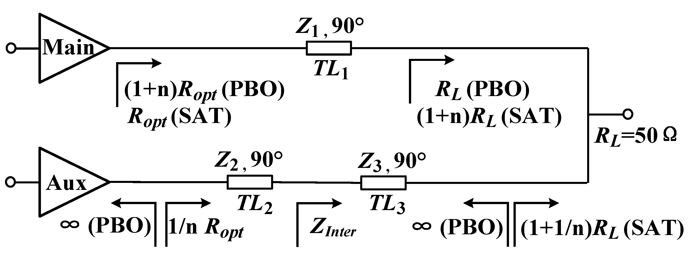
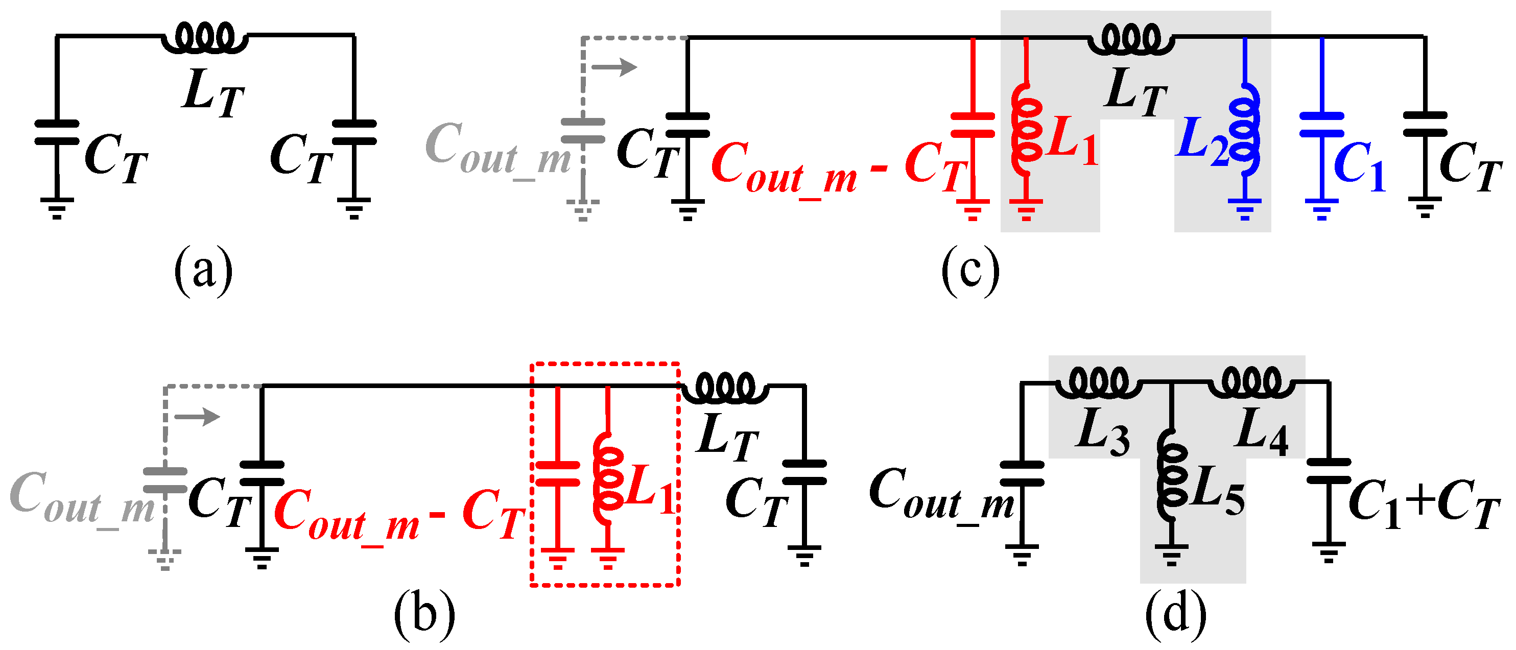
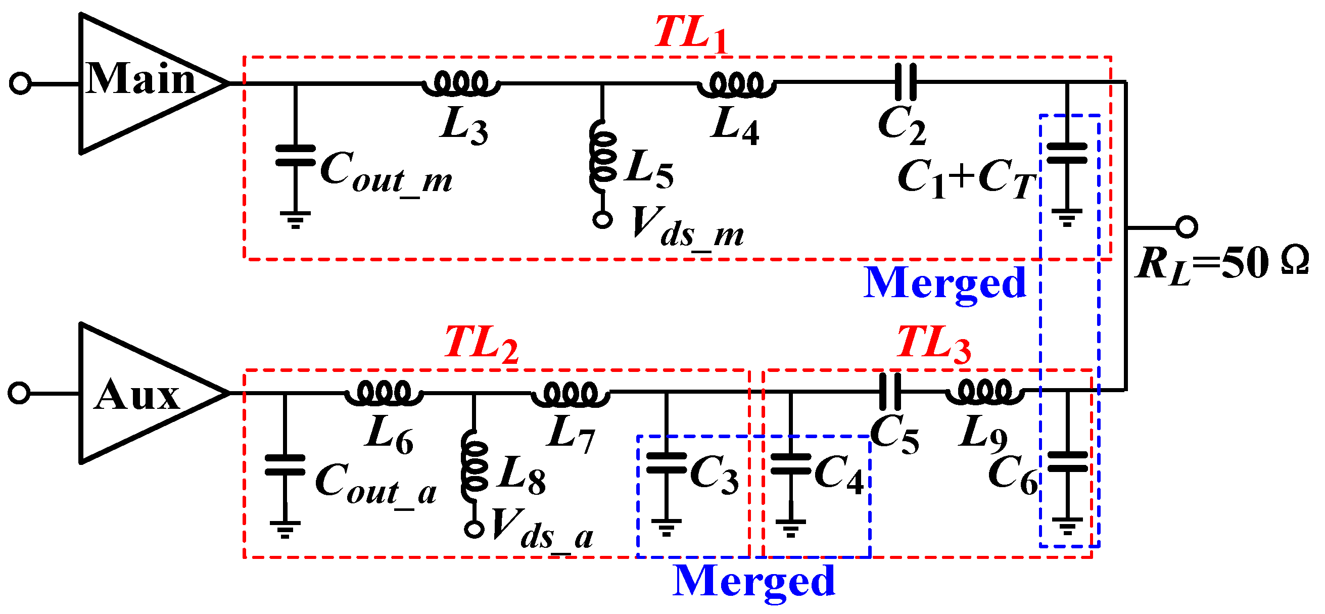
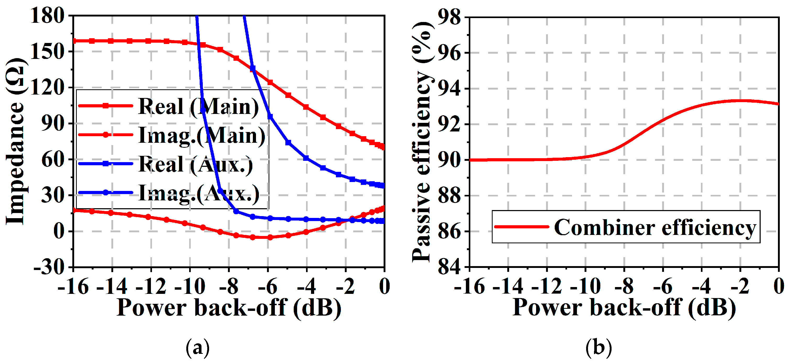
2.1. Analysis and Design of the Output Combiner

To achieve better efficiency and bandwidth performance, a Doherty power combiner structure based on three quarter-wave transmission lines was selected, as illustrated in Figure 2. Considering that there were two quarter-wave transmission lines following the auxiliary power amplifier in this structure, the impedance at the combination point could be directly set to 50 Ω, regardless of the optimal load impedance Ropt of the main power amplifier. This eliminated the necessity for a post-matching network. The n in the figure refers to the ratio of the transistor size between the auxiliary power amplifier and the main power amplifier.
The impedance of each node of the main and auxiliary power amplifiers in the saturation and back-off regions is marked in Figure 2. The characteristic impedance of the quarter-wave transmission line TL1 could be obtained as follows:
Z 1 = ( 1 + n ) R L R o p t
To obtain the widest bandwidth, the impedance of the middle node of the two quarter-wavelength lines after the auxiliary power amplifier was selected as follows [7,8]:
Z I n t e r = ( 1 + 1 / n ) R L × R o p t n = ( 1 + n ) R L R o p t n
Therefore, the characteristic impedance of the quarter-wave transmission lines TL2 and TL3 could be obtained as follows:
Z 2 = R o p t Z I n t e r n
Z 3 = ( 1 + 1 / n ) R L × Z I n t e r = ( 1 + n ) R L Z I n t e r n

2.2. Design Procedure of the Combiner

Considering that a large size of transmission lines is not conducive to implementation inside a PA module of miniaturized size, we hereby propose to use lumped components to achieve the above structure.
Taking quarter-wave transmission line TL1 after the main power amplifier as an example, it can be modeled by a π-type network at the center frequency of f0, as shown in Figure 3a. The component values of the LT and CT are calculated as follows [9]:
L T = Z 1 2 π f 0
C T = 1 2 π f 0 Z 1
The output capacitance of the main PA Cout_m is absorbed into the impedance transformation network to reduce its degradation of bandwidth [10]. According to the load–pull results for the main PA, the Cout_m is larger than the required CT. Therefore, a short inductor L1 is needed to resonate out the remaining Cout_mCT as shown in Figure 3b. The inductance of the L1 can be calculated as follows:
L 1 = 1 ( 2 π f 0 ) 2 ( C o u t _ m C T )
Due to the particularity of the module form, the first matching component of the impedance transformation network must be a series bonding-wire inductor. Therefore, the impedance transformation network must be transformed from a π-type network to a T-type network. To make up for the π-type network, an LC resonant network is inserted into the impedance transformation network as shown in Figure 3c. The capacitance C1 and the inductance L2 can be designed to have a parallel resonance at the operating frequency f0:
f 0 = 1 2 π L 2 C 1
By applying a Δ-Y transformation, the structure of the impedance transformation network is presented in Figure 3d. The corresponding relationships between the inductance values before and after the transformation are as follows:
L 3 = L T × L 1 L T + L 1 + L 2
L 4 = L T × L 2 L T + L 1 + L 2
L 5 = L 1 × L 2 L T + L 1 + L 2
From Equations (9)–(11), it can be seen that, after transforming from the π-type network to the T-type network, the inductance values of L3L5 decrease compared to L1, LT, and L2, respectively. For SMDs, smaller inductance values result in a higher quality factor and a higher rated current, making the T-type network more conducive to achieving a high-performance DPA module. The most critical parameter among the above is L3, which is limited by the design rules of the bonding wire. Therefore, it needs to be designed to a reasonable value first. Next, based on the load–pull results and Equations (1)–(11), the parameters of the entire impedance transformation network can be determined.
The analysis method of using lumped components to replace transmission line TL2 is similar to that of TL1. The transmission line TL3 is equivalenced by adopting a π-type network. The final DPA output combiner is depicted in Figure 4. Inductors L5 and L8 serve as power supply inductors for the main and auxiliary power amplifiers, respectively. Capacitors C2 and C5 serve as DC-block capacitors. The shunt-lumped capacitors at the same node can be merged to simplify the circuit. The simulated load impedances and the passive efficiency of the proposed combiner are plotted in Figure 5. It can be observed that the proposed combiner maintains a passive efficiency of more than 90% while realizing the desired Doherty active-load modulation. In our study, the passive efficiency was simulated as the output power on the load divided by the sum of powers from the main and auxiliary transistor devices delivered into the combiner. All SMDs were simulated using model data provided by the manufacturer with the limited Q value.

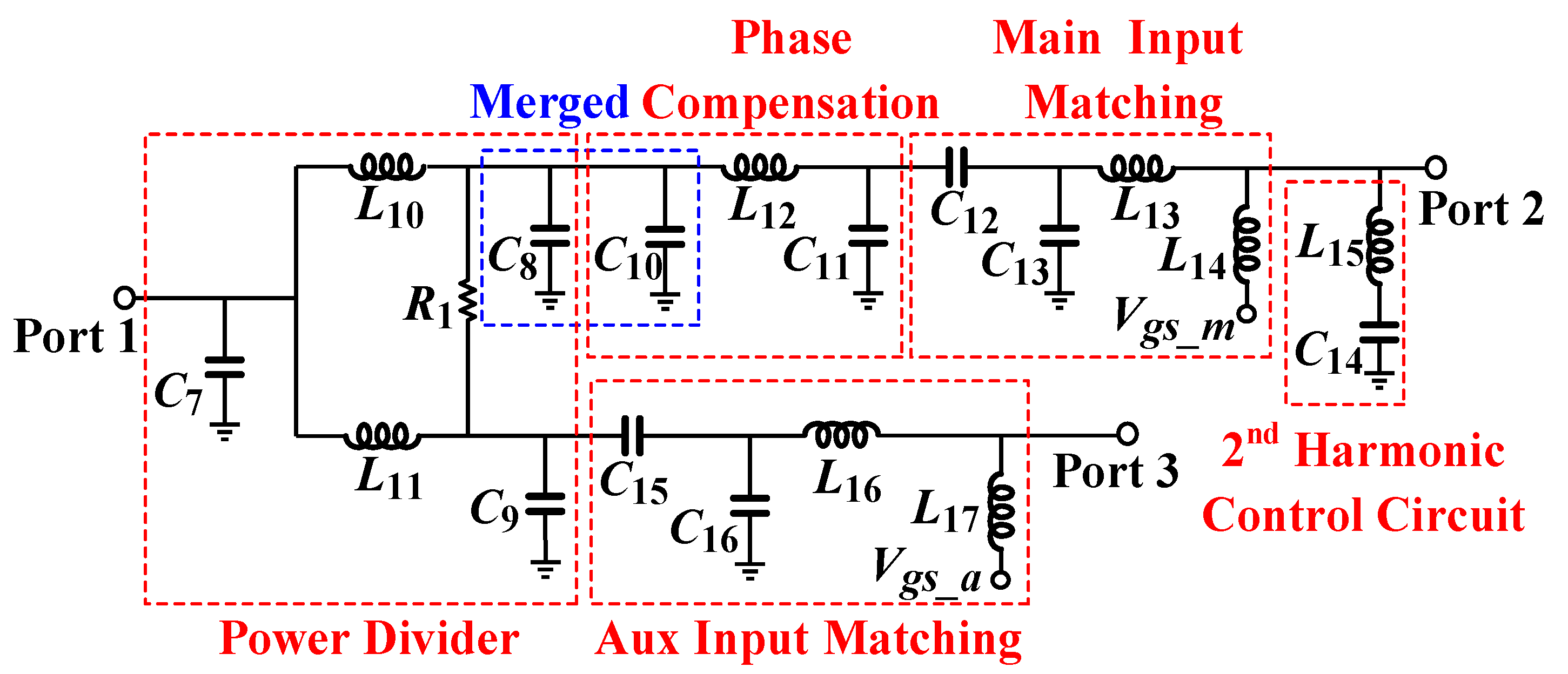
2.3. Design of Input Matching and Power Divider

The input matching network and the power divider of the DPA module are depicted in Figure 6. The input matching of the main amplifier and the auxiliary amplifier both adopt a multistage band-pass network to expand the bandwidth. A π-type phase compensation network is inserted in the input path of the main PA to align the phase of the main PA and the auxiliary PA at the combination node.
A Wilkinson divider created using lumped components is used for power splitting. The shunt-lumped capacitors at the same node can be merged. A second harmonic control circuit is inserted at the input of the main power amplifier for high efficiency [11]. In addition, a driver stage PA is connected to the input of the Wilkinson power divider for high gain.

3. Implementation and Measurement Results

The proposed two-stage Doherty PA module was fabricated on polyimide substrate using GaN transistors and SMDs, as shown in Figure 7. The size of this Doherty PA module was only 8 × 8 mm2, including the driver amplifier, main PA, and auxiliary PA. The drain bias voltages of the driver, the main PA, and the auxiliary PA were all set to 23 V. The main amplifier and driver amplifier were both biased at Class-AB mode, and the auxiliary amplifier was biased at Class-C mode. The performance of the Doherty PA module was characterized by small-signal, large-signal, and modulated-signal measurements.

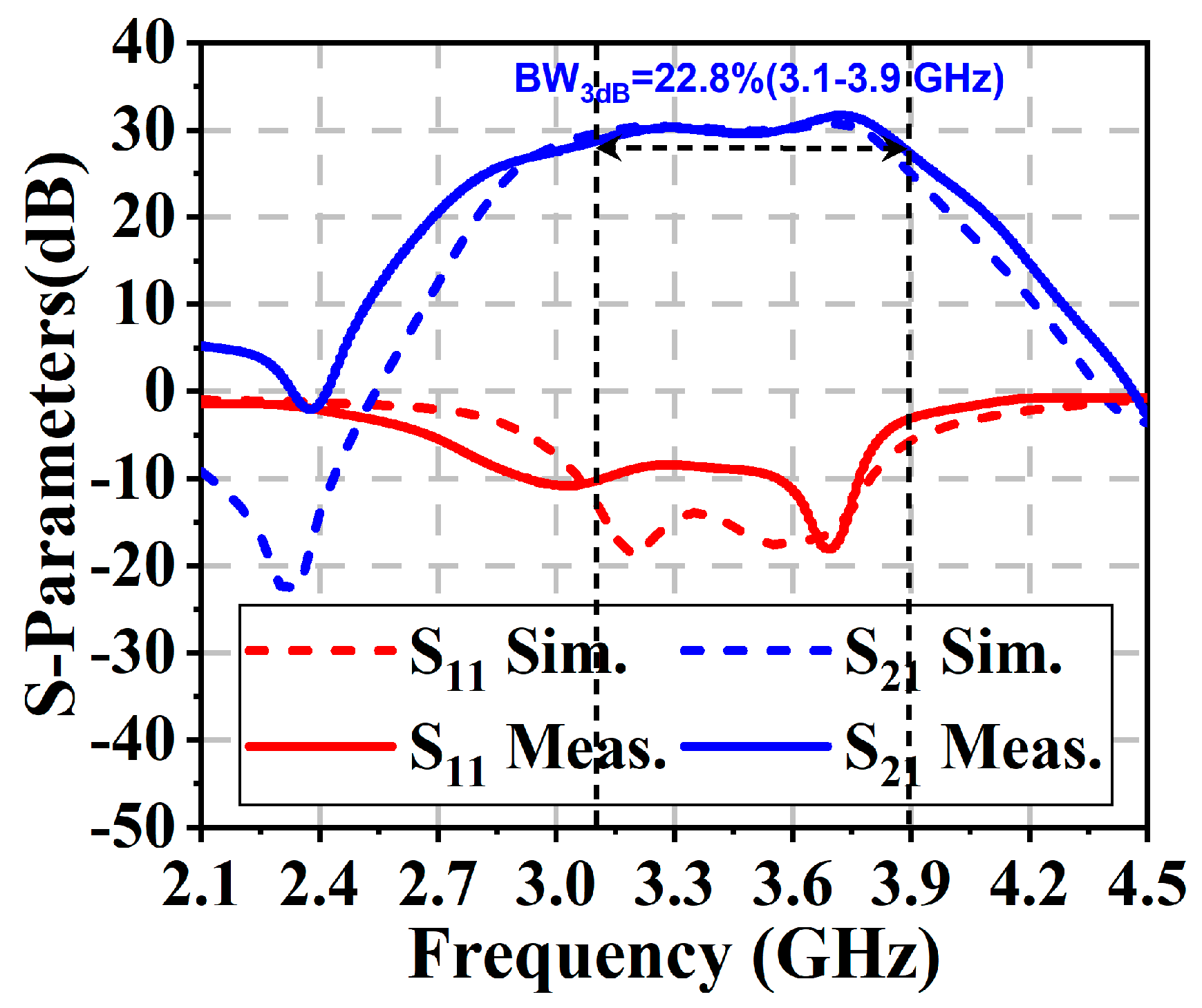
3.1. Small-Signal Measurement

Figure 8 compares the simulated S11/S21 parameters with the measured ones. Good agreement can be observed between the simulation and measurement results. The proposed two-stage DPA achieved a 3 dB small-signal bandwidth of 3.1–3.9 GHz and a peak gain of 31.7 dB at 3.71 GHz. The gain fluctuation within 3.2–3.6 GHz was less than 0.8 dB. The measured return loss was about −10 dB within the target band.

3.2. Large-Signal Measurement

The large-signal performance of the fabricated DPA module was evaluated using pulsed continuous-wave (CW) signal. According to Figure 9a, the proposed two-stage Doherty PA could achieve 40.4–41.1 dBm saturated output power at 3.2–3.6 GHz. The measured saturated DE and 8 dB PBO DE reached 51–56.6% and 45.5–48.6%, respectively. Figure 9b presents the measured drain efficiency and power gain versus output power, respectively. Table 1 summarizes the performance of the proposed DPA module together with state-of-the-art GaN DPA modules/MMICs for 5G base station applications for comparison.
The fabricated two-stage DPA module exhibited excellent comprehensive performance, including the back-off DE, gain, and bandwidth. Compared to state-of-the-art GaN DPA modules/MMICs, the proposed two-stage DPA module exhibited the highest back-off DE, including during the driver stage.

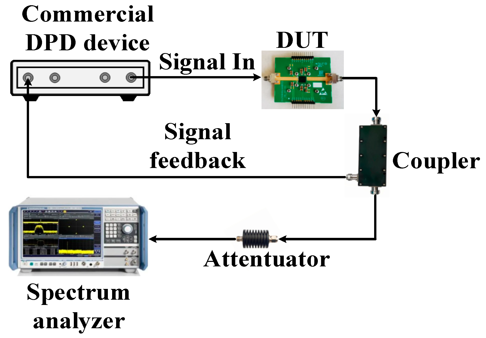
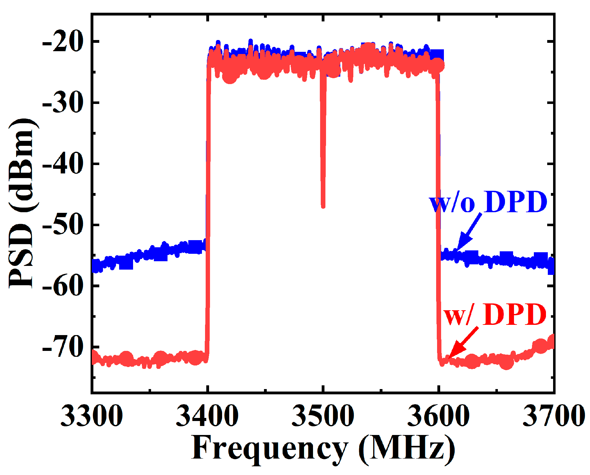
3.3. Modulated-Signal Measurement

The experimental setup for the modulated measurements is presented in Figure 10. A commercial digital pre-distortion (DPD) device designed for small-cell base stations was utilized to evaluate the linearity performance of the proposed DPA module. The modulated-signal measurements were carried out using a two-carrier 200 MHz 5G NR signal with a PAPR of 8.8 dB. The DPA module was operated at 10.2 dB back-off to deliver 30.7 dBm average output power and 38.9% drain efficiency at 3.5 GHz. Figure 11 depicts the power spectral density (PSD) of the DPA module’s output signal with and without DPD linearization. Before DPD, the fabricated DPA module achieved good original linearity with a −32.1/−33 dBc adjacent channel leakage ratio (ACLR) performance, which could be improved to −49.2/−48.3 dBc after DPD linearization.

4. Conclusions

In this paper, the design procedure and measurements of a high-performance two-stage Doherty PA module are presented, satisfying the requirements of a 5G application. The DPA module is implemented by GaN transistors and SMDs on polyimide substrate with an LGA package size of 8 × 8 mm2. The DPA module achieves a small-signal gain of 29.6–30.4 dB and a saturated output power of 40.4–41.1 dBm in the frequency range of 3.2–3.6 GHz. From 3.2 to 3.6 GHz, the designed DPA module provides 51% to 56.6% DE at saturation output power and 45.5% to 48.6% DE at 8 dB of output power back-off. When feeding a two-carrier 200 MHz 5G NR signal, the DPA module achieves a DE of 38.9% at an average output power of 30.7 dBm at 3.5 GHz. The ACLR performance can be improved from −32.1/−33 dBc to −49.2/−48.3 dBc through DPD linearization. Compared to state-of-the-art GaN DPA modules/MMICs, the fabricated two-stage DPA module exhibits excellent comprehensive performance, including peak DE, back-off DE, gain, and bandwidth.

Author Contributions

Conceptualization, D.W.; data curation, X.L. and K.C.; methodology, X.W.; project administration, W.L. and H.L.; validation, X.W.; writing—original draft, D.W.; and writing—review and editing, K.K. All authors have read and agreed to the published version of the manuscript.

Funding

This research received no external funding.

Data Availability Statement

The original contributions presented in the study are included in the article, further inquiries can be directed to the corresponding author.

Conflicts of Interest

The authors declare no conflicts of interest. Authors Xiyu Wang, Dehan Wang, Wenming Li, Xiaolin Lv, Kai Cui, and Haijun Liu are employed by the company ZTE Corporation. All the authors declare that the research was conducted in the absence of any commercial or financial relationships that could be construed as potential conflicts of interest.

References

  1. Doherty, W.H. A New High Efficiency Power Amplifier for Modulated Waves. Proc. IRE 1936, 24, 1163–1182. [Google Scholar] [CrossRef]
  2. Musolff, C.; Kamper, M.; Abou-Chahine, Z.; Fischer, G. A Linear and Efficient Doherty PA at 3.5 GHz. IEEE Microw. Mag. 2013, 14, 95–101. [Google Scholar] [CrossRef]
  3. Chen, W.; Lv, G.; Liu, X.; Wang, D.; Ghannouchi, F.M. Doherty PAs for 5G massive MIMO: Energy-efficient integrated DPA MMICs for sub-6-GHz and mm-wave 5G massive MIMO systems. IEEE Microw. Mag. 2020, 21, 78–93. [Google Scholar] [CrossRef]
  4. Sakata, S.; Kato, K.; Teranishi, E.; Sugitani, T.; Ma, R.; Chuang, K.; Wu, Y.-C.; Fukunaga, K.; Komatsuzaki, Y.; Horiguchi, K.; et al. A Fully-Integrated GaN Doherty Power Amplifier Module with a Compact Frequency-Dependent Compensation Circuit for 5G massive MIMO Base Stations. In Proceedings of the IEEE MTT-S International Microwave Symposium (IMS), Los Angeles, CA, USA, 4–6 August 2020; pp. 711–714. [Google Scholar]
  5. Liu, R.-J.; Zhu, X.-W.; Xia, J.; Chen, P.; Yu, C.; Zhang, L.; Chen, Z.Y. A 30-W GaN Quasi-MMIC Doherty Power Amplifier Based on All-Distributed Inductors Load Network. In Proceedings of the 51st European Microwave Conference (EuMC), London, UK, 4–6 April 2022; pp. 946–949. [Google Scholar]
  6. Sakata, S.; Taguchi, M.; Kato, K.; Teranishi, E.; Honda, S.; Komatsuzaki, Y.; Tsuru, M.; Yamanaka, K. A 3.4–4.1 GHz Broadband GaN Doherty Power Amplifier Module for 5G massive-MIMO Base-Stations. In Proceedings of the Asia-Pacific Microwave Conference (APMC), Yokohama, Japan, 29 November–2 December 2022; pp. 500–502. [Google Scholar]
  7. Giofrè, R.; Piazzon, L.; Colantonio, P.; Giannini, F. A Closed-Form Design Technique for Ultra-Wideband Doherty Power Amplifiers. IEEE Trans. Microw. Theory Tech. 2014, 62, 3414–3424. [Google Scholar] [CrossRef]
  8. Barakat, A.; Thian, M.; Fusco, V.; Bulja, S.; Guan, L. Toward a More Generalized Doherty Power Amplifier Design for Broadband Operation. IEEE Trans. Microw. Theory Tech. 2017, 65, 846–859. [Google Scholar] [CrossRef]
  9. Kuylenstierna, D.; Gunnarsson, S.E.; Zirath, H. Lumped-element quadrature power splitters using mixed right/left-handed transmission lines. IEEE Trans. Microw. Theory Tech. 2005, 53, 2616–2621. [Google Scholar] [CrossRef]
  10. Gustafsson, D.; Cahuana, J.C.; Kuylenstierna, D.; Angelov, I.; Rorsman, N.; Fager, C. A Wideband and Compact GaN MMIC Doherty Amplifier for Microwave Link Applications. IEEE Trans. Microw. Theory Tech. 2013, 61, 922–930. [Google Scholar] [CrossRef]
  11. Jee, S.; Lee, J.; Son, J.; Kim, S.; Kim, C.H.; Moon, J.; Kim, B. Asymmetric Broadband Doherty Power Amplifier Using GaN MMIC for Femto-Cell Base-Station. IEEE Trans. Microw. Theory Tech. 2015, 63, 2802–2810. [Google Scholar]
  12. Lv, G.; Chen, W.; Liu, X.; Feng, Z. A Dual-Band GaN MMIC Power Amplifier With Hybrid Operating Modes for 5G Application. IEEE Microw. Wireless Compon. Lett. 2019, 29, 228–230. [Google Scholar] [CrossRef]
  13. Seidel, A.; Wagner, J.; Ellinger, F. 3.6 GHz Asymmetric Doherty PA MMIC in 250 nm GaN for 5G Applications. In Proceedings of the German Microwave Conference (GeMiC), Cottbus, Germany, 9–11 March 2020; pp. 1–4. [Google Scholar]
  14. Lv, G.; Chen, W.; Chen, X.; Wan, S.; Ghannouchi, F.M.; Feng, Z. A Fully Integrated 3.5-/4.9-GHz Dual-Band GaN MMIC Doherty Power Amplifier Based on Multi-Resonant Circuits. IEEE Trans. Microw. Theory Tech. 2022, 70, 416–431. [Google Scholar] [CrossRef]
  15. Oh, H.; Choi, W.; Shin, J.; Chen, Y.; Kang, H.; Woo, Y.Y.; Yang, Y. A 6-/12-dB Back-off Multi-Mode GaN MMIC Doherty Power Amplifier for 5G Applications. In Proceedings of the IEEE MTT-S International Microwave Symposium (IMS), San Diego, CA, USA, 11–16 June 2023; pp. 458–461. [Google Scholar]
Figure 1. Circuit topology of the two-stage Doherty PA module designed using GaN transistors and SMDs.
Micromachines 16 00220 g001
Figure 2. Doherty PA combiner structure based on three quarter-wave transmission lines.
Micromachines 16 00220 g002
Figure 3. Design procedure of the TL1 implemented with lumped components: (a) quarter-wave transmission line modeled by a π-type network; (b) π-type network with Cout_m absorbed; (c) inserting LC resonant network to prepare for the next step; and (d) use Δ-Y conversion to obtain a T-type network.
Micromachines 16 00220 g003
Figure 4. The schematic of the proposed compact and low-loss combiner.
Micromachines 16 00220 g004
Figure 5. (a) Simulated load impedance of the proposed combiner at 3.4 GHz. (b) Passive efficiency of the combiner during load modulation at 3.4 GHz.
Micromachines 16 00220 g005
Figure 6. The input matching network and power divider of the DPA module.
Micromachines 16 00220 g006
Figure 7. Photograph of the fabricated two-stage DPA module before molding.
Micromachines 16 00220 g007
Figure 8. Measured and simulated S-parameters.
Micromachines 16 00220 g008
Figure 9. (a) Pulsed CW measurements of Psat, peak, and 8 dB back-off DE. (b) Measured DE and gain versus output power at different frequencies.
Micromachines 16 00220 g009
Figure 10. Modulated-signal measurement setup.
Micromachines 16 00220 g010
Figure 11. Output PSD with and without DPD at 3.5 GHz.
Micromachines 16 00220 g011
Table 1. Comparison with state-of-the-art 3.5 GHz GaN Doherty PAs.
Ref.Freq.(GHz)Gain (dB)Psat (dBm)DE@OPBO (%)StageArea (mm2)Type
This work3.2–3.629.6–30.440.4–41.145.5–48.6
@8dB OPBO
28 × 8SMD
Module
[3]3.4–3.826.9–28.637.7–38.542.9–47.8 *
@8dB OPBO
210 × 6SMD + IPD
Module
[4]3.4–3.810.5–12 **44.4–45.145–49
@8dB OPBO
15.6 × 4.3IPD
Module
[5]3.4–4.131.747.942–44.6 *
@8dB OPBO
276Module
[12]3.3–3.81241.8–42.642–51
@6dB OPBO
12.4 × 2.4MMIC
[13]3.4–3.711.738.840–46 *
@8.5dB OPBO
110MMIC
[14]3.35–3.612.1–12.343.8–44.741–46
@6dB OPBO
12.8 × 3.5MMIC
[15]3.3–3.611 **42.6–4334.7–39
@6dB OPBO
13.3 × 3.2MMIC
* PAE. ** Graphically estimated.
Disclaimer/Publisher’s Note: The statements, opinions and data contained in all publications are solely those of the individual author(s) and contributor(s) and not of MDPI and/or the editor(s). MDPI and/or the editor(s) disclaim responsibility for any injury to people or property resulting from any ideas, methods, instructions or products referred to in the content.

