Article

Studies on Electronic Structure and Optical Properties of MoS2/X (X = WSe2, MoSe2, AlN, and ZnO) Heterojunction by First Principles

by
Jibo Liu
1,2,
Yuheng Jin
3,
Bocheng Lei
1,
Xucai Zhao
1,
Yineng Huang
1,
Lili Zhang
1,* and
Youliang Zhu
1,4,*
1
Xinjiang Laboratory of Phase Transitions and Microstructures in Condensed Matters, College of Physical Science and Technology, Yili Normal University, Yining 835000, China
2
College of Information Science and Engineering, Xinjiang College of Science & Technology, Kuerle 841000, China
3
School of Physics, Sichuan University, Chengdu 610065, China
4
State Key Laboratory of Supramolecular Structure and Materials, College of Chemistry, Jilin University, Changchun 130023, China
*
Authors to whom correspondence should be addressed.
Catalysts 2024, 14(10), 678; https://doi.org/10.3390/catal14100678
Submission received: 14 August 2024 / Revised: 16 September 2024 / Accepted: 26 September 2024 / Published: 1 October 2024
(This article belongs to the Special Issue Photocatalytic Nanomaterials for Environmental Purification)

Abstract

:
The single-layer MoS2 is a highly sought-after semiconductor material in the field of photoelectric performance due to its exceptional electron mobility and narrow bandgap. However, its photocatalytic efficiency is hindered by the rapid recombination rate of internal photogenerated electron–hole pairs. Currently, the construction of heterojunctions has been demonstrated to effectively mitigate the recombination rate of photogenerated electron–hole pairs. Therefore, this paper employs the first principles method to calculate and analyze the four heterojunctions formed by MoS2/WSe2, MoS2/MoSe2, MoS2/AlN, and MoS2/ZnO. The study demonstrates that the four heterojunctions exhibit structural stability. The construction of heterojunctions, as compared to a monolayer MoS2, leads to a reduction in the band gap, thereby lowering the electron transition barrier and enhancing the light absorption capacity of the materials. The four systems exhibit II-type heterojunction. Therefore, the construction of heterojunctions can effectively enhance the optical properties of these systems. By forming heterojunctions MoS2/WSe2 and MoS2/MoSe2, the absorption coefficient in the visible light region is significantly increased, resulting in a greater ability to respond to light compared to that of MoS2/ZnO and MoS2/AlN. Consequently, MoS2-based heterojunctions incorporating chalcogenide components WSe2 and MoSe2, respectively, exhibit superior catalytic activity compared to MoS2 heterojunctions incorporating non-chalcogenide components ZnO and AlN, respectively. The absorption spectrum analysis reveals that MoS2/MoSe2 exhibits the highest light responsivity among all investigated systems, indicating its superior photoelectric performance.

1. Introduction

Due to their high electron mobility, surface activity, and narrow band gap, two-dimensional transition metal dichalcogenides (2D-TMDs) are extensively found in various applications such as photodetectors, optoelectronic devices, and photocatalysts [1,2]. The monolayer MoS2 belongs to the family of 2D-TMDs and has a sandwich structure consisting of S-Mo-S [3,4,5]. The monolayer MoS2 has significant potential in the fields of photocatalysts and optoelectronic devices, such as low power field effect transistors [6], valley electronics devices [7] and photodetectors [8], owing to its straightforward preparation process, favorable band gap structure, and exceptional magnetic and optical properties [9,10]. However, the limited application efficiency of the monolayer MoS2 in the aforementioned optoelectronic devices stems from its low absorption of incident and high recombination rate of photogenerated electron–hole pairs [7,8]. Consequently, current research efforts are primarily directed towards identifying effective strategies to enhance the absorption of visible light by the monolayer MoS2 and mitigate electron–hole pair recombination within the system.
Modulating the properties of two-dimensional materials through the construction of two-dimensional heterojunctions connected by van der Waals (vdW) force represents a commonly employed strategy. These heterojunctions give rise to electronic and optical properties that can surpass those of monolayer components, as evidenced by previous research [11,12,13,14]. In particular, the ones of the heterojunctions exhibit a type II band structure, which could induce an internal electric field that lowers the recombination probability of electron–hole pairs. As a result, constructing type II heterojunctions is a popular choice for photoelectric devices [15,16]. Deng et al. [17] used a first principles approach to investigate CdTe/MoS2 heterojunctions. They found that constructing heterojunctions effectively promoted the separation of photogenerated carriers, which improved the photoelectron conversion efficiency and made the system suitable for high-efficiency photodetector material. The successful preparation of the MoS2/CuO heterojunction [18], BP/MoS2 heterojunction [19], and MoS2/MAPbBr3 [20] has demonstrated the effectiveness of type II heterojunctions in modulating the band gap and enhancing the system’s response to light. Constructing a new type II heterojunction holds significant value. Despite previous experimental [13] and theoretical [21] studies on MoS2-based heterojunctions, delving deeper into the microscopic mechanism of these heterojunctions remains a scientific pursuit of great importance.
Monolayer MoSe2 and monolayer WSe2 are semiconductors known for their high optical conversion efficiency, making them ideal materials for optoelectronic devices such as light-emitting diodes [22,23] and solder effect transistors [24,25]. Additionally, they share similar structures and properties with other broad-band semiconductors such as monolayers MoS2, ZnO, and AlN, which are representative materials for constructing type II heterojunctions. Using MoS2 as a base, this study will compare the difference in heterostructures built with other selenium-based compounds, such as MoSe2 and WSe2, to those compounds like ZnO and AlN [26,27]. In MoS2/MoSe2 and MoS2/WSe2, each monolayer is a sulfur-based compound, but in MoS2/ZnO and MoS2/AlN, ZnO and AlN are not sulfur-based compounds. To date, no theoretical investigation has been conducted on the differences in optical properties between these two types.
In this study, the heterojunction construction of WSe2, MoSe2, AlN, and ZnO based on the monolayer MoS2 will offer additional options for the application of MoS2-based heterojunctions and a theoretical reference for specific experimental preparation in materials for optoelectronic devices.

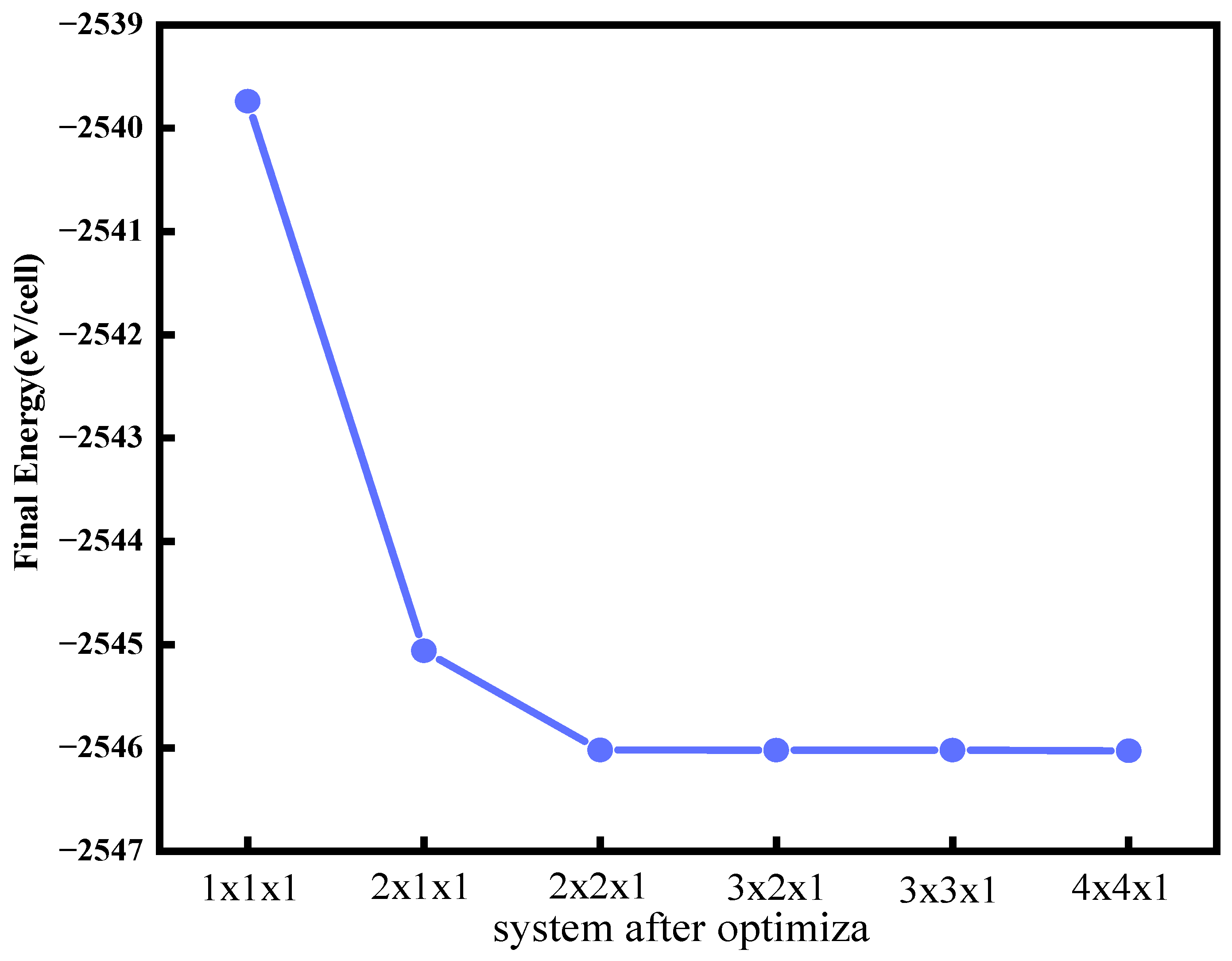
2. Computational Methods and Theoretical Model

The calculation program employed in this study is CASTEP (Cambridge Serial Total Energy Package) module in the Materials Studio 2017, which is based on density functional theory. The interaction between ions and electrons is described by the projected plane wave method using plane wave as the base group. The exchange correlation potential between electrons is described using the PBE (Perdew–Burke–Ernzerhof) exchange–correlation generalized gradient approximation [28,29]. The interlayer vans der Waals forces are corrected by the TS (Tkachenko–Scheffler) dispersion method in the calculations [30,31]. The electron configurations of atoms involved in this paper are Mo: 4d55s1, S: 3s23p4, Se: 4s24p4, Al: 3s23p1, N: 2s22p3, Zn: 3d104s2, and O: 2s22p4. After conducting convergence tests, the cutoff energy of is set to 450 eV, and the Brillouin Zone-K grid point is chosen as 5 × 5 × 1. To eliminate boundary effects and interface effects, periodic boundary conditions are adopted in the x-direction and y-direction and a fixed boundary is adopted in the z-direction. Additionally, to reduce the potential interlayer mutual coupling effects, a vacuum layer with a thickness of 20 angstroms is embedded along the Z-direction between the two layers of each heterojunction. The self-consistent convergence accuracy is set to 2.0 × 10⁻⁵ eV/atom, with a maximum stress limit of 0.1 GPa. Additionally, the maximum displacement is restricted to less than 2 × 10⁻³ Å, and the interatomic force field convergence accuracy is set to 0.05 eV/Å. All the calculations are based on the BFGS (Broyden–Fletcher–Goldfarb–Shanno) algorithm.
In the heterojunction structure designed in this paper, factors such as interface effects and boundary effects are considered. The two materials are designed in a vertical structure stacked up and down in the form of thin films. The relatively simple structure ensures the performance of the device. Based on the convergence test diagram (Figure 1), the supercell size of MoS2 is set to 3 × 3 × 1, which ensures calculation accuracy while conserving computing resources. To match with the substrate MoS2, the supercell size of WSe2, MoSe2, AlN, and ZnO in the four heterojunctions is also set to 3 × 3 × 1. The calculation of heterojunction energy for five stacking modes is as shown in the Supplementary Material (Figure S1), naming them from SP1 to SP5, respectively. The stacking mode SP1 exhibits the lowest ground state energy, as demonstrated by Figure S1. This finding indicates that mode SP1 possesses the most stable structure, thus justifying its selection in our paper. The constructed MoS2/X (X = WSe2, MoSe2, AlN, and ZnO) four heterojunction models are shown in Figure 2.

3. Geometric Parameters and System Stability

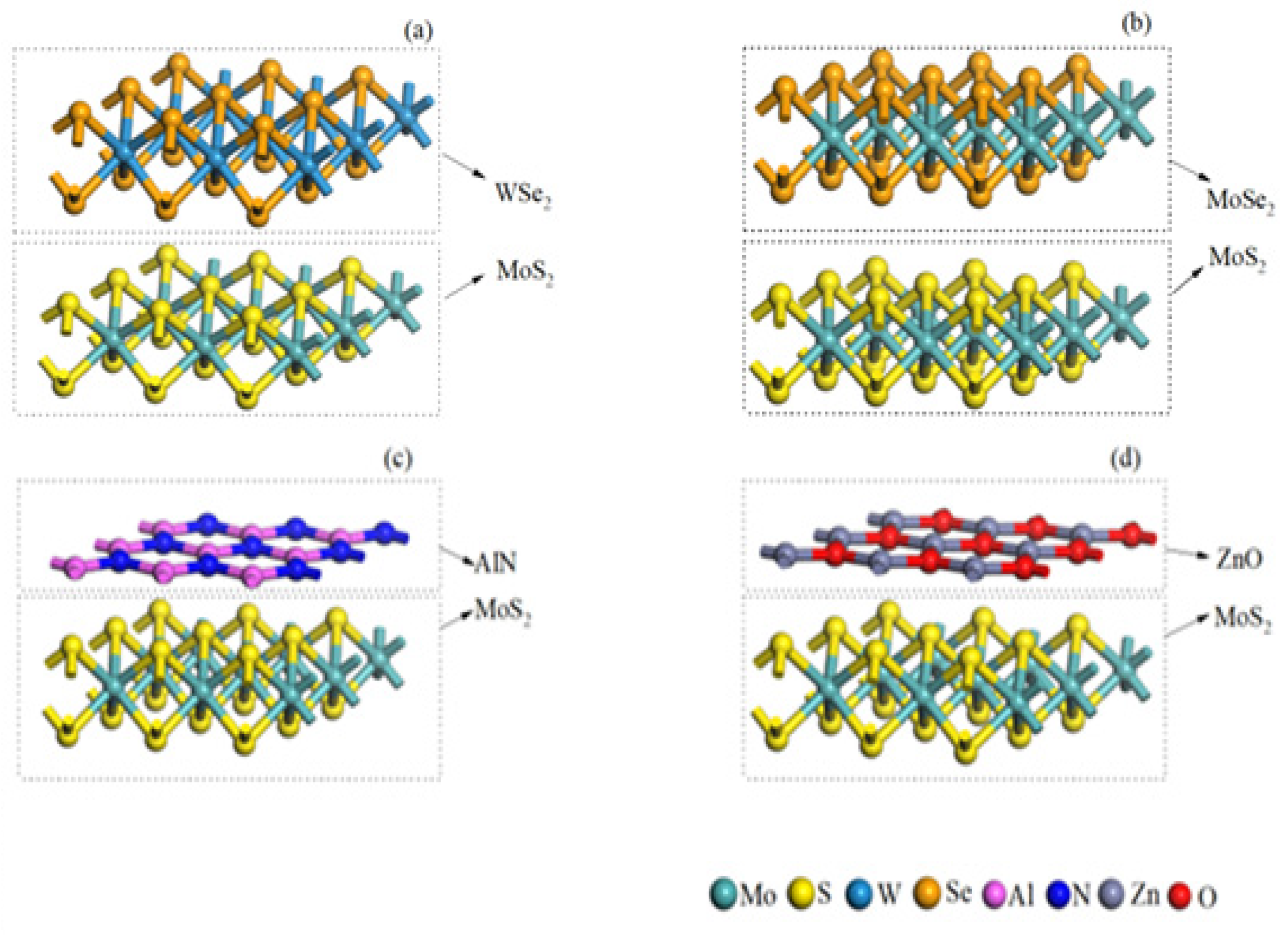
3.1. Geometric Parameters

Before constructing heterojunctions, we geometrically optimize the monolayers MoS2, WSe2, MoSe2, AlN, and ZnO. During the optimization process, the c-axis was fixed, and the lattice constants and atomic positions in other directions were relaxed. The optimized lattice constant for each system is presented in Table 1. The results indicate that the optimized lattice constants agree well with theoretical values, confirming the reliability and validity of the selected calculation parameters.

3.2. Stability

To investigate the heterogeneous lattice matching, we assign the lattice constants of monolayers MoS2 and X as a1 and a2, respectively. Next, we calculate the lattice mismatch rates in the four systems and represent them using Equation (1) [37].
σ = ( a 1 a 2 ) a 1
The lattice mismatch rates of the four systems are calculated to be 4.02% for MoS2/WSe2, 3.83% for MoS2/MoSe2, 1.61% for MoS2/AlN, and 2.43% for MoS2/ZnO. These values satisfy the complete co-lattice condition (δ < 5%), indicating that all four heterojunctions are potential stable structures [38].
In order to quantitatively assess the lattice mismatch and structural stability of the four heterojunctions, we have conducted calculations for the lattice mismatch energy Δ(Emis), binding energy (Eb), and van der Waals energy (ΔEvdw) using Equations (2)–(4) [39,40,41].
Δ E mis = 1 S E MoS 2 1 + E X 1 E MoS 2 2 E X 2
E b = E sum E MoS 2 2 E X 2
E(MoS2)1 and E(X)1 are the total energies of the isolated monolayer MoS2 and isolated monolayer X, respectively. E(MoS2)2 and E(X)2 represent the total energy of the MoS2 and X in a heterojunction, respectively. Additionally, S represents the area of a heterojunction layer. The stability of a heterojunction is indirectly assessed by both ΔEsum and Eb. A smaller lattice mismatch energy indicates a more stable structure, while a smaller binding energy suggests tighter binding [38]. Table 2 displays the calculated results, which indicate that the lattice mismatch energy and binding energy of the four systems are negative. MoS2/AlN exhibits the smallest lattice mismatch energy and binding energy, indicating that the heterojunction is the most stable system. It is found that the four systems, WSe2, MoSe2, AlN, and ZnO, can form a stable heterojunction with MoS2.
In order to further verify the thermal stability of these, The DS - PAW [42] module in the Device Studio 2023 first principles plane wave calculation software was used to simulate the ab initio molecular dynamics (AIMDs) of the four systems at 300 K (equivalent to room temperature). The calculation is based on the canonical ensemble NVT (canonical ensemble with particles N, volume V, and temperature T) and is performed using the Nosé–Hoover method. Ref. [43], as shown in Figure 3, provides an example. It evident that the structures of the four structures remain stable even after 8000 steps of AIMDs with a step size of 1 fs, as no atomic bond is broken and the energy fluctuations are minimal. The results demonstrate that MoS2/X exhibits exceptional high stability at ambient temperature (300 K).

4. Electronic Structure

4.1. Energy Band Structure

To facilitate a comparative analysis of the electronic structures among various heterojunctions, this study computationally determines the energy band structure diagrams for the monolayer MoS2 and four distinct heterojunctions, namely MoS2/WSe2, MoS2/MoSe2, MoS2/AlN, and MoS2/ZnO. The Fermi energy level (Ef) is set at 0 eV, as shown in Figure 4a–e. The diagram in Figure 4a illustrates that both the conduction band minimum (CBM) and the valence band maximum (VBM) correspond to the high symmetry point K, thereby demonstrating the direct band structure of single-layer MoS2. The calculated band gap value of 1.75 eV exhibits a negligible deviation of only 0.5% from the experimental value of 1.76 eV [44], thereby affirming the reliability and reasonability of the parameters and methodologies employed in this study.
The band gap of the four heterojunctions, namely MoS2/WSe2, MoS2/MoSe2, MoS2/AlN, and MoS2/ZnO, are 0.50 eV, 0.67 eV, 1.05 eV, and 0.60 eV, respectively (Figure 4b–e). Additionally, all heterojunctions still exhibit a direct band structure. The band gaps of all heterojunctions have been reduced compared to that of the monolayer MoS2, facilitating the electron transitions and enhancing light absorption efficiency. Notably, the MoS2/WSe2 band gap experiences the most significant reduction.
The band structure in MoS2/AlN and MoS2/ZnO exhibits a relatively low density of states due to the significantly wider bandgaps of AlN and ZnO compared to that of single-layer MoS2. Consequently, upon combination, there is a shift towards deeper energy levels in both conduction and valence bands. And it can be seen from the figure that the density on the conduction band of the two heterojunctions of MoS2/WSe2 and MoS2/MoSe2 is greater than that of MoS2/AlN and MoS2/ZnO, which may be because the components of both heterojunctions of MoS2/WSe2 and MoS2/MoSe2 are chalcogen compounds, and after combination, electrons are more likely to transfer from the valence band to the conduction band. The band diagrams reveal that the four heterojunctions demonstrate a type II band alignment. Further analysis on this aspect will be discussed subsequently.

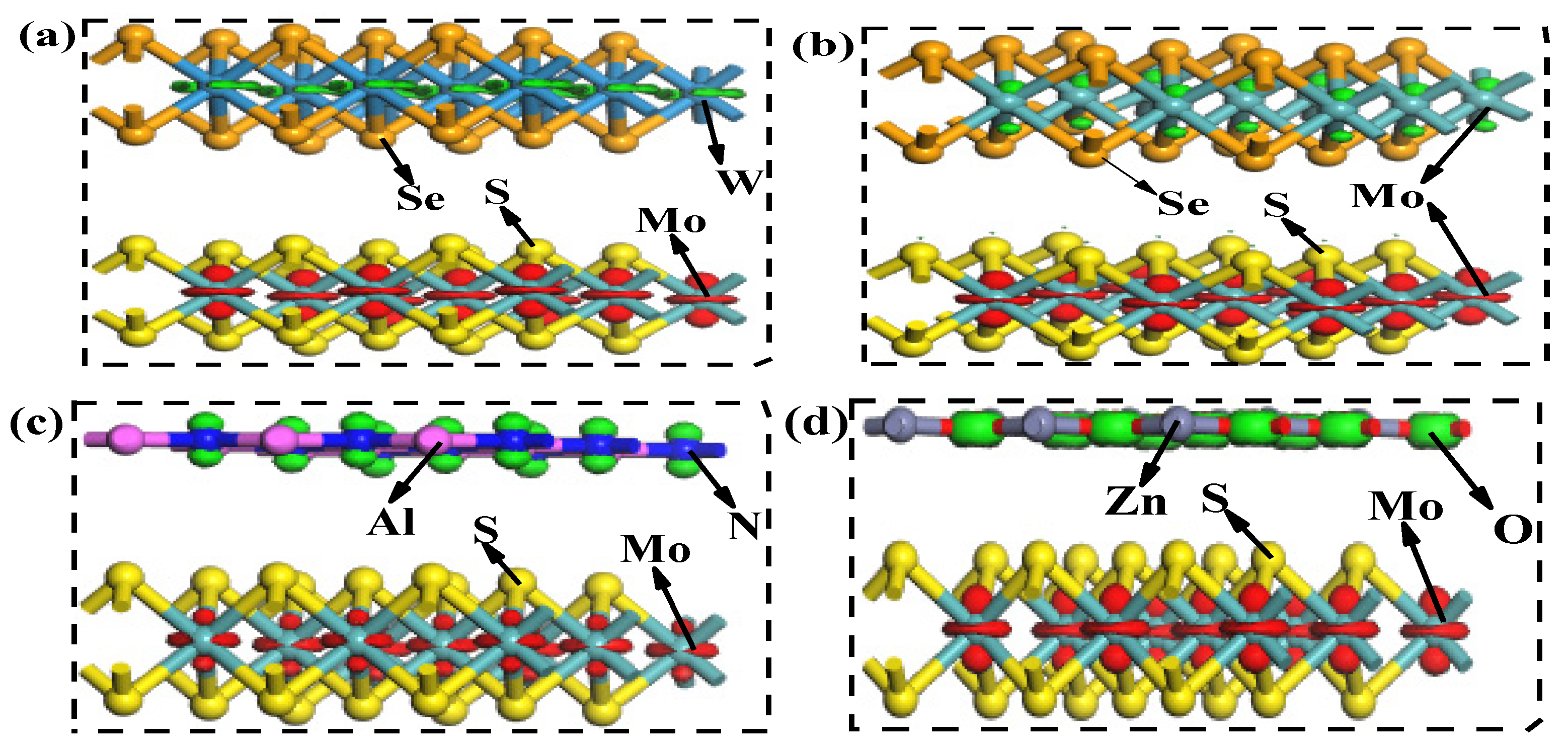
4.2. Density of States
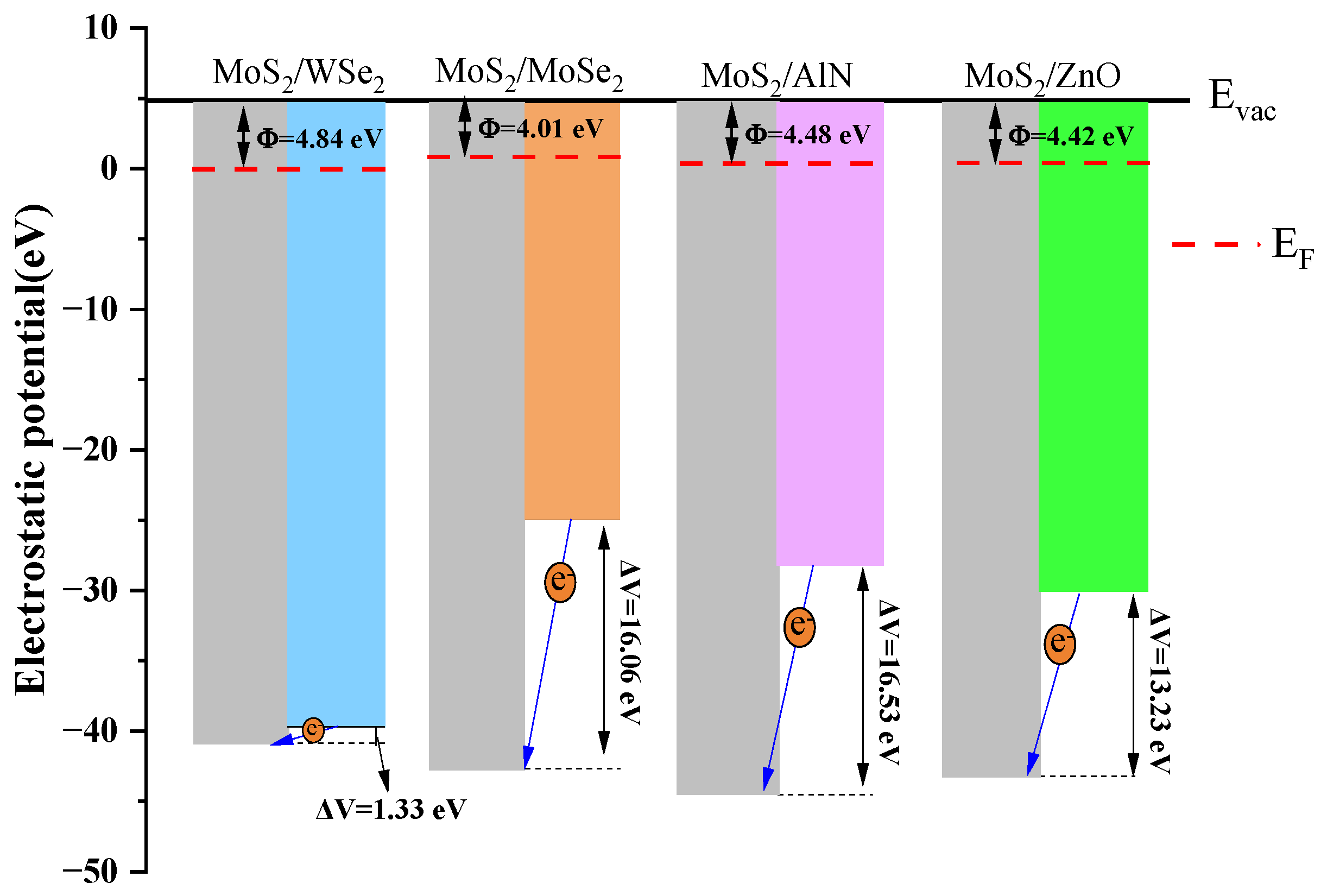
The density of state plots for the monolayer MoS2 with four heterojunctions are presented in Figure 5. The conduction band of the monolayer MoS2 is primarily constituted of Mo-4d, Mo-5s, and S-3p states, while the valence band predominantly consists of Mo-4d, S-3s, and S-3p states, as illustrated in Figure 5a. The Fermi energy level of the system intersects the valence band and is slightly situated below the VBM. The main reason for this phenomenon is attributed to the disruption of the periodic potential field in the system caused by cutting the bulk phase structure, leading to the formation of the monolayer MoS2. This phenomenon leads to the generation of a continuous energy distribution at the uppermost region of the valence band, thereby inducing a band tail effect. The density of states of MoS2/WSe2 is presented in Figure 5b. The VBM of the heterojunction is found to arise from the spatial distribution of the Se-4p orbital within WSe2, while CBM originates from the spatial distribution of the Mo-5s orbital within MoS2. The density of states of MoS2/MoSe2 depicted in Figure 5c. The VBM of the heterojunction arises from the hybridization between Mo-5s orbitals and Se-4p orbitals in MoSe2, while the CBM is primarily attributed to the Mo-5s orbitals of MoS2. The density of states of the MoS2/AlN is illustrated in Figure 5d. The VBM of the heterojunction is predominantly contributed to by the N-2p orbitals of AlN, while the CBM is mainly contributed to by the Mo-5s orbitals of MoS2. The density of states of MoS2/ZnO is depicted in Figure 5e. The O-2p orbital in ZnO predominantly contributes to the VBM of the heterojunction, whereas the Mo-5s orbital in the MoS2 primarily governs the CBM.
Combined with the energy band structure diagram, it can be observed that the VBMs of all four heterojunctions are predominantly contributed to by the X material, while the CBMs primarily arise from energy states associated with MoS2. The VBM and CBM originate from distinct materials within the heterojunction, exhibiting characteristic features of typical type II heterojunctions [45,46]. It is evident that all four heterojunctions possess type II band alignments.
The conduction bands of all four heterojunctions exhibit a pronounced overlap in energy levels from the S-3p and Mo-5s orbitals of MoS2. The strong orbital hybridization between S and Mo atoms is indicative of enhanced electron transfer from S-3p orbitals to Mo-5s orbitals, facilitating the movement of excited electrons. Consequently, the heterojunction facilitates a higher concentration of electrons at Mo atoms within the MoS2 material. In heterojunctions, the degree of overlap between different orbitals in the density of state diagrams varies, resulting in a potential reduction in the band gap magnitude within the systems. This reduction in the band gap can enhance the light absorption efficiency of the system, as evidenced by the analysis of energy band diagrams.

4.3. Work Function

The work function(Φ), as defined by Equation (5), quantifies the energy required to overcome the surface potential barrier, enabling electrons to escape from the solid surface (EF) and reach the vacuum energy level (Evac). This function offers valuable insights into the photoelectric emission efficiency of the semiconductor, which is pivotal for comprehending its electronic characteristics and potential applications.
Φ = E vac E F
Table 3 demonstrates that the calculated work function is higher than the experimental value, which can be attributed to the tendency of GGA calculations to overestimate the work function. The calculated work function results presented in this study are generally consistent with recently published findings, thereby establishing the credibility of our calculations. Since the calculated results are solely utilized for comparative analysis of heterojunctions in this study, their relative trends can be considered reliable [47,48,49,50,51,52,53,54,55,56].
The direction of electron transfer in the four heterojunctions can be tentatively determined as follows: electrons will migrate from the WSe2 layer to the MoS2 layer, from the AlN layer to the MoS2 layer, and from the ZnO layer to the MoS2 layer. The statement is derived from the analysis of work function images in various systems.
The simplified diagram illustrating the work function in Figure 6 reveals that the heterojunctions generate an internal electric field due to the disparity between each two constituents. The internal electric field serves to enhance the efficiency of separation of photogenerated electrons and holes, thereby augmenting the photoelectric functionality of the systems. This observation is consistent with the findings obtained from the electric structure analysis.
The analysis above indicates that electron transfer occurs at the interface of the heterojunction. To investigate the microscopic details of electron transfer, Figure 7 presents diagrams illustrating the lowest unoccupied molecular orbital (LUMO) and highest occupied molecular orbital (HOMO) of the four heterojunctions.
The electrons in the LOMO possess the minimum energy and exhibit enhanced accessibility to the external environment. Conversely, electrons residing in the HOMO demonstrate elevated energy levels but limited binding capacity, thereby facilitating facile electron loss. When subjected to solar irradiation, photoexcited electrons undergo a transition from the LUMO state to the HOMO state, thereby establishing the LUMO–HOMO transition as the primary pathway for the migration of photogenerated electrons [57,58,59]. Figure 7 indicates that the LUMO and HOMO of the four heterojunctions are located in distinct components. Therefore, the presence of an internal electric field within the heterojunction is observed to facilitate a reduction in the recombination rate of electron–hole pairs. This observation is also in line with the analysis of the internal electric field in type II heterojunctions.
Considering the results presented in Figure 7a–d, it is evident that electron transfer takes place from the W atoms in the WSe2 layer to the Mo atoms in the MoS2 layer within MoS2/WSe2. Similarly, in MoS2/MoSe2, the electrons transfer from Mo atoms in the MoSe2 layer to Mo atoms in the MoS2 layer. In MoS2/AlN, the transfer flow is from N atoms in the AlN layer to Mo atoms in the MoS2 layer. In MoS2/ZnO, electrons transfer from O atoms in the ZnO layer to Mo atoms in the MoS2 layer. Consequently, at the heterojunction interface, the transfer of electrons results in the formation of an internal electric field, and the field in the four heterojunctions are all directed towards MoS2. As a result, the photoelectric properties of the four systems are enhanced, which is in line with the findings from the work function analysis.

5. Optical Property

5.1. Alignment with Edges

Typically, photocatalysts are assessed based on the semiconductor conduction band (CB) and valence band (VB) values relative to the standard hydrogen electrode (NHE). To determine the band edge potential on the NHE scale, Equations (5) and (6) [58] are commonly used. In semiconductor physics, X represents the absolute electronegativity of the material. The free electron energy at the NHE scale, which is approximately 4.5 eV, is denoted by Eelce. Meanwhile, Eg refers to the semiconductor band gap.
E CB = X E elec 0.5 E g
E VB = VBM + E g
The study calculated the ECB and EVB values for the monolayer MoS2 and four heterojunctions, namely MoS2/WSe2, MoS2/MoSe2, MoS2/AlN, and MoS2/ZnO. The values obtained were (0.055 eV, 1.695 eV), (−0.75 eV, 0.25 eV), (0.005 eV, 0.675 eV), (−0.545 eV, 0.505 eV), and (−0.380 eV, 0.22 eV), respectively. The photocatalytic mechanism of the material involves the absorption of photon energy, which causes the transfer of electrons (e) in the VB to CB, leaving holes (h+) in the VB. The resulting e-h+ pairs participate in the redox reaction to degrade pollutants. In this paper, it is observed that all the systems studied, namely the monolayer MoS2, MoS2/WSe2, MoS2/MoSe2, MoS2/AlN, and MoS2/ZnO, have the capability to absorb photon energy and generate e-h+ for redox reactions. Additionally, the construction of heterojunctions has been found to alter the photocatalytic ability of the monolayer MoS2. The monolayer MoS2 has a higher ECB than the O2/·O2− reduction potential of −0.33 eV [59]. Therefore, it cannot directly produce ·O2−. However, through the construction of heterojunctions, the ECB is effectively reduced. This reduction occurs in three heterojunctions, according to [60]; the monolayer MoS2 has a higher ECB than the O2/·O2− reduction potential of −0.33 eV, which means that it cannot directly produce O2−. However, it is possible to reduce the ECB effectively by constructing heterojunctions. This reduction can occur in three different heterojunctions.
E CB vac = E CB 4.5
E VB vac = E VB 4.5
E H + / H 2 red = 4.44   eV + PH × 0.059   eV
E O 2 / H 2 O oxd = 5.67   eV + PH × 0.059   eV
To ensure a photocatalyst’s versatility, we evaluated the vacuum band edge potential of five systems against NHE and the redox potential of water at varying pH levels using Equations (7)–(10) [60]. The resulting data are presented in Figure 8. Research has indicated that the monolayer MoS2 is not suitable for hydrogen precipitation in environments that are either acidic, neutral, or basic. In MoS2/MoSe2, the conduction band minimum (CBM) is similar to that of the monolayer MoS2. However, the valence band (VB) is not lower than the potential of O2/H2O. This means that electrons in the CB can combine with O2 to form ·O2, which allows the heterojunction to retain some of the inherent photocatalytic properties of the monolayer MoS2.

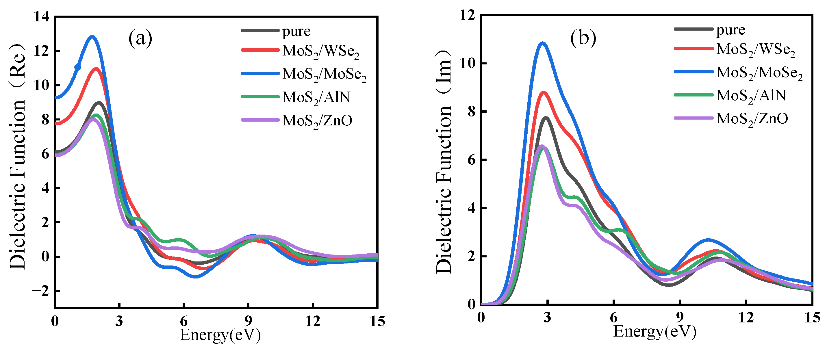
5.2. Complex Dielectric Function

The intricate dielectric functions for the monolayer MoS2 and four heterojunctions are depicted in Figure 9. Specifically, Figure 9a illustrates the real component of the dielectric function, with the point of intersection on the vertical axis denoting the static dielectric constant of the five systems [61]. The values obtained for the systems are 5.80, 7.81, 9.30, 5.81, and 5.79, respectively. The static dielectric constants of the four heterojunctions are observed to surpass that of the monolayer MoS2, thereby demonstrating enhanced polarization ability, intensified photogenerated electric field intensity, and accelerated carrier migration rates. These enhancements contribute to the efficient separation of photogenerated electron–hole pairs. MoS2/MoSe2 exhibits the highest static dielectric constant, indicating its superior polarization capability. In Figure 9b, the curves represent the imaginary component of the dielectric functions, and the first peaks of all the curves corresponds to electron transitions between the conduction band and valence band. The transverse coordinate value corresponding to the peak value is equivalent to the band gap width [62]. The primary peak of the monolayer MoS2 is observed at 2.92 eV. Meanwhile, the primary peaks of the four heterojunctions, namely MoS2/WSe2, MoS2/MoSe2, MoS2/AlN, and MoS2/ZnO, are located at 2.80 eV, 2.77 eV, 2.83 eV, and 2.74 eV, respectively. In comparison to the monolayer MoS2, the heterojunctions exhibit the shift of its main peaks towards the low-energy direction, indicating a smaller band gap value. Additionally, the figure illustrates that MoS2/MoSe2 exhibits the highest peak in the imaginary part of the dielectric functions, which can be attributed to a hybridization effect between Mo-5s and S-3p orbitals.

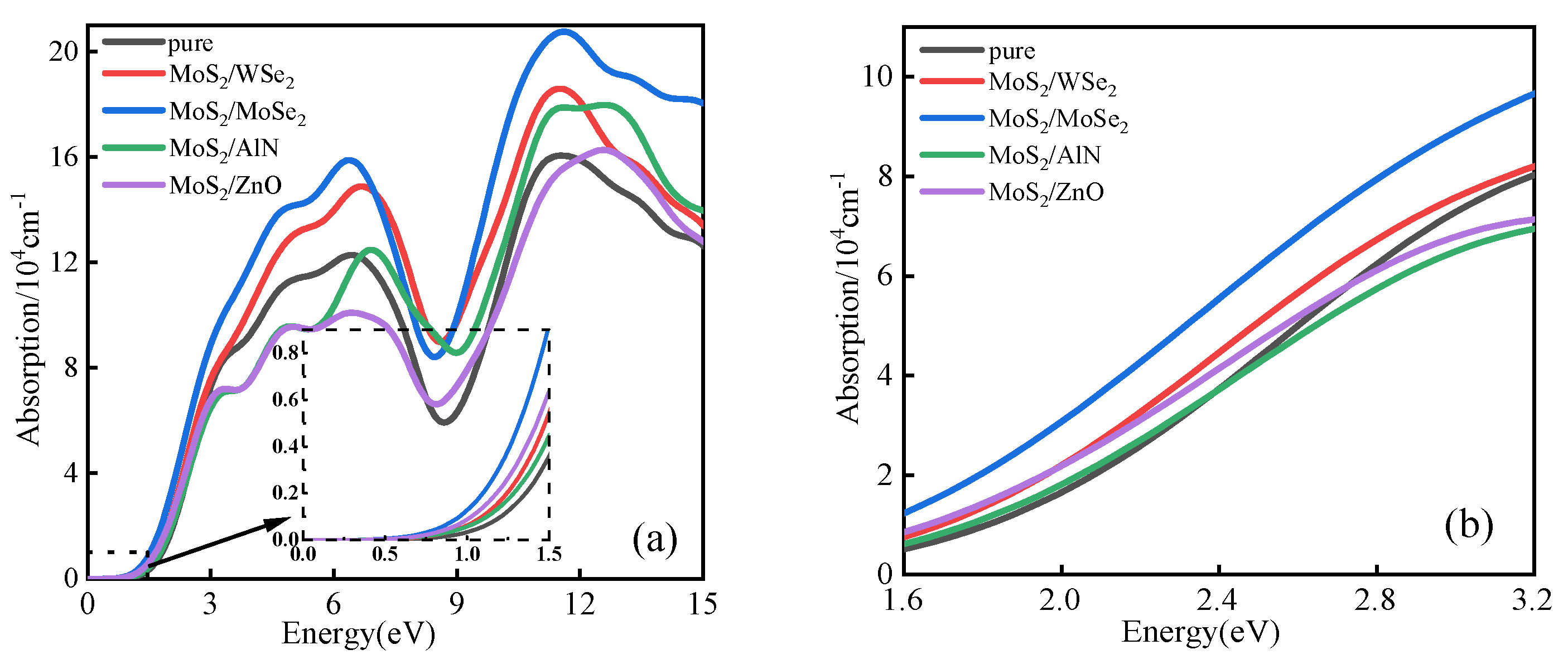
5.3. Absorption Spectrum

The semiconductor light absorption coefficient is denoted by α. This parameter quantifies the ability of the system to absorb light, with its magnitude reflecting the strength of this capability [61,62].
α ω = 2 ω k ω c
In the equation, ω stands for angular frequency, k(ω) represents the complex refractive index, and c denotes the speed of light.
The absorption spectra of the monolayer MoS2 and four heterojunctions are illustrated in Figure 10a,b, providing insights into the energy-dependent trend in the optical absorption coefficient within the photon energy range of 0–15 eV. The inset of Figure 10a reveals a red shift in the optical absorption band edges of the four heterojunctions compared to the monolayer MoS2, indicating that the formation of heterojunctions can effectively broaden the system’s spectral response range to light. The absorption spectra of all five systems show similar trends varying with photon energy, featuring more pronounced absorption peaks compared to the monolayer MoS2 at intervals of 5–7 eV and 10–11 eV, while the MoS2/MoSe2 structure exhibited the highest peak.
To enhance the practicality of the data, we additionally generated absorption spectra for the five systems within the visible region (1.6–3.2 eV), as depicted in Figure 10b. The absorption coefficients of the four heterojunctions in the visible region have increased compared to that of the monolayer MoS2. MoS2/MoSe2 demonstrates the highest absorption coefficient within the visible region, indicating its superior capacity for absorbing visible light.

6. Conclusions

The electronic structure and optical properties of four new heterostructures, MoS2/WSe2, MoS2/MoSe2, MoS2/AlN, and MoS2/ZnO, which are constructed with MoS2 as the substrate, are calculated by the density functional theory. The constructed heterostructures have been observed to exhibit a stable existence, with a type II band structure and a band gap smaller than that of the monolayer. The generation of the MoS2 type II band structure implies that the internal electric field generates at the interface of the four heterojunctions, enhancing the effective separation of photogenerated electron–hole pairs. The conclusion has been substantiated by means of an analysis conducted on the absorption spectrum and dielectric function. The heterostructures MoS2/WSe2, MoS2/MoSe2, and MoS2/AlN exhibit a redshift absorption spectrum compared to the monolayer MoS2, thereby expanding the systems’ range of light response, and they have stronger static dielectric constants than that of the monolayer MoS2. In addition, MoS2/WSe2 and MoS2/MoSe2 in the visible region have higher absorption coefficients and static dielectric constants than that of MoS2/AlN and MoS2/ZnO, indicating that the light absorption capacity of chalcogenide heterojunctions is superior. Chalcogenide heterojunctions MoS2/WSe2 and MoS2/MoSe2 have a stronger electronic transition ability and are more suitable for optical electronic devices.

Supplementary Materials

The following supporting information can be downloaded at: https://www.mdpi.com/article/10.3390/catal14100678/s1, Figure S1. Stacking pattern of heterojunctions. SP1 is the alignment of tungsten (W) and molybdenum (Mo); SP2 is the alignment of selenium (Se) and molybdenum (Mo); SP3, SP4, and SP5 are stacking patterns with different angles between selenium (Se) and molybdenum (Mo).

Author Contributions

Conceptualization, X.Z., L.Z. and Y.Z.; methodology, J.L., Y.H. and Y.Z.; validation, J.L. and Y.Z.; formal analysis, B.L.; investigation, J.L. and X.Z.; data curation, J.L., Y.J. and B.L.; writing—original draft preparation, J.L. and X.Z.; writing—review and editing, Y.H., L.Z. and Y.Z.; visualization, X.Z. and Y.J.; project administration, L.Z.; funding acquisition, L.Z. All authors have read and agreed to the published version of the manuscript.

Funding

This research was funded by the Open Project of Xinjiang Laboratory of Condensed Matter Phase Transition and Microstructure, grant number XJDX0912Y2409, the Science and Technology Plan Project of Yili Kazakh Autonomous Prefecture, grant number YZ2022B021, and the key project at the school level of Yili Normal University, grant number 2023YSZD003.

Data Availability Statement

The original contributions presented in the study are included in the article; further inquiries can be directed to the corresponding authors.

Acknowledgments

We gratefully acknowledge HZWTECH for providing computation facilities.

Conflicts of Interest

The authors declare no conflicts of interest.

References

  1. Mak, K.F.; Shan, J. Photonics and optoelectronics of 2D semiconductor transition metal dichalcogenides. Nat. Photonics 2016, 10, 216–226. [Google Scholar] [CrossRef]
  2. García-Dalí, S.; Paredes, J.I.; Villar-Rodil, S.; Martínez-Jódar, A.; Martínez-Alonso, A.; Tascón, J.M.D. Molecular Functionalization of 2H-Phase MoS2 Nanosheets via an Electrolytic Route for Enhanced Catalytic Performance. ACS Appl. Mater. Int. 2021, 13, 33157–33171. [Google Scholar] [CrossRef] [PubMed]
  3. Lu, S.; Li, C.; Zhao, Y.F. Tunable redox potential of nonmetal doped monolayer MoS2: First principle calculations. Appl. Surf. Sci. 2016, 384, 360–367. [Google Scholar] [CrossRef]
  4. Lin, S.Y.; Li, W.T.; Dong, Y.Y.; Wang, C.; Chen, Q.; Zhang, H. Two-dimensional metallic MoS2: A DFT study. Comput. Mater. Sci. 2016, 124, 49–53. [Google Scholar] [CrossRef]
  5. Shirazi, M.; Kessels, W.M.M.; Bol, A.A. Initial stage of atomic layer deposition of 2D-MoS2 on a SiO2 surface: A DFT study. Phys. Chem. Chem. Phys. 2018, 20, 16861. [Google Scholar] [CrossRef]
  6. Yoon, Y.; Ganapathi, K.; Salahuddin, S. How Good Can Monolayer MoS2 Transistors Be? Nano Lett. 2011, 11, 3768–3773. [Google Scholar] [CrossRef]
  7. Mak, K.F.; He, K.; Shan, J.; Heinz, T.F. Control of valley polarization in monolayer MoS2 by optical helicity. Nat. Nanotechnol. 2012, 7, 494–498. [Google Scholar] [CrossRef]
  8. Lopez-Sanchez, O.; Lembke, D.; Kayci, M.; Radenovic, A.; Kis, A. Ultrasensitive photodetectors based on monolayer MoS2. Nat. Nanotechnol. 2013, 8, 497–501. [Google Scholar] [CrossRef]
  9. Zhuang, H.L.; Hennig, R.G. Computational Search for Single-Layer Transition-Metal Dichalcogenide Photocatalysts. J. Phys. Chem. C 2013, 117, 20440–20445. [Google Scholar] [CrossRef]
  10. Schmidt, H.; Wang, S.; Chu, L. Transport Properties of Monolayer MoS2 Grown by Chemical Vapor Deposition. Nano Lett. 2014, 14, 1909–1913. [Google Scholar] [CrossRef]
  11. Li, S.S.; Sun, J.R.; Guan, J.Q. Strategies to improve electrocatalytic and photocatalytic performance of two-dimensional materials for hydrogen Strategies to improve electrocatalytic and photocatalytic performance of two-dimensional materials for hydrogen evolution reaction. Chin. J. Catal. 2021, 42, 511–556. [Google Scholar] [CrossRef]
  12. Liu, Y.; Cao, Y.; Lv, H.; Li, S.; Zhang, H. Construction of a 2D nanoplate-like MoS2/Bi2WO6 heterojunction with enhanced visible-light photocatalytic activities. Mater. Lett. 2017, 188, 99–102. [Google Scholar] [CrossRef]
  13. Yu, Z.; Peng, J.; Lei, H.; Zhai, X.F.; Jiang, F.H.; Sun, C.J. Novel Z-scheme MoS2/Bi2WO6 heterojunction with highly enhanced photocatalytic activity under visible light irradiation. J. Alloys Compd. 2021, 8, 157224. [Google Scholar]
  14. Liao, J.; Zhong, Y.; He, Z.; Ding, H.; Chen, K.; Chen, D.M. One-step synthesis of MoS2/Bi2S3 heterojunction with enhanced photocatalytic activity and high electrochemical performance. J. Mater. Sci. Mater. Electron. 2020, 32, 385–394. [Google Scholar] [CrossRef]
  15. Zhang, X.; Xia, M.; Wang, F.; Lei, W. Cu2O/MoS2 composites: A novel photocatalyst for photocatalytic degradation of organic dyes under visible light. Ionics 2020, 31, 6359–6369. [Google Scholar] [CrossRef]
  16. Yao, H.; Guo, X.; Bao, A.; Mao, H.Y.; Ma, Y.C.; Li, X.C. Graphene-based heterojunction for enhanced photodetectors. Chin. Phys. B 2022, 31, 38501. [Google Scholar] [CrossRef]
  17. Deng, X.Z.; Zhang, J.R.; Zhao, Y.Q.; Yu, Z.L.; Yang, J.L.; Cai, M.Q. The energy band engineering for the high-performance infrared photodetectors constructed by CdTe/MoS2 heterojunction. J. Phys. Condens. Matter 2020, 32, 65004. [Google Scholar] [CrossRef]
  18. Um, D.; Lee, Y.; Lim, S.; Park, S.Y.; Lee, C.; Ko, H. High-Performance MoS2/CuO Nanosheet-on-One-Dimensional Heterojunction Photodetectors. ACS Appl. Mater. Interfaces 2016, 8, 33955–33962. [Google Scholar] [CrossRef]
  19. Abderrahmane, A.; Woo, C.; Ko, P.J. Black Phosphorus/Molybdenum Diselenide Heterojunction-Based Photodetector. J. Electron. Mater. 2021, 50, 5713–5720. [Google Scholar] [CrossRef]
  20. Meng, F.X.; Xu, Z.Q.; Zeng, Y.H.; Wang, C.H.; Zou, Y.N.; Wageh, S.; Al-Ghamdi, A.; Guo, Z.N.; Zhang, H. Photodetectors Based on MoS2/MAPbBr3 van der Waals Heterojunction. IEEE Electron Device Lett. 2022, 43, 414–417. [Google Scholar] [CrossRef]
  21. Xue, Z.; Zhang, X.; Qin, J.; Liu, R.P. Constructing MoS2/g-C3N4 heterojunction with enhanced oxygen evolution reaction activity: A theoretical insight. Appl. Surf. Sci. 2019, 5, 254–268. [Google Scholar] [CrossRef]
  22. Sundaram, R.S.; Engel, M.; Lombardo, A.; Krupke, R.; Ferrari, A.C.; Avouris, P.; Steiner, M. Electroluminescence in Single Layer MoS2. Nano Lett. 2013, 13, 1416–1421. [Google Scholar] [CrossRef] [PubMed]
  23. Ye, L.; Wang, P.; Luo, W.J.; Gong, F.; Liao, L.; Liu, T.D.; Tong, L.; Zang, J.F.; Xu, J.B.; Hu, W.D. Highly polarization sensitive infrared photodetector based on black phosphorus-on-WSe2 photogate vertical heterostructure. Nano Energy 2017, 37, 53–60. [Google Scholar] [CrossRef]
  24. Zhou, X.; Tian, Z.; Kim, H.J.; Wang, J.; Xu, B.R.; Pan, R.B.; Chang, Y.J.; Di, Z.F.; Zhou, P.; Mei, Y.F. Rolling up MoSe2 Nanomembranes as a Sensitive Tubular Photodetector. Small 2019, 15, 1902528. [Google Scholar] [CrossRef] [PubMed]
  25. Roy, T.; Tosun, M.; Hettick, M.; Ahn, G.H.; Hu, C.M.; Javey, A. 2D-2D tunneling field-effect transistors using WSe2/SnSe2 heterostructures. Appl. Phys. Lett. 2016, 108, 83111. [Google Scholar] [CrossRef]
  26. Dybaa, F.; Polak, M.P.; Kopaczek, J.; Scharoch, P.; Wu, K.; Tongay, S.; Kudrawiec, R. crystals and semiconductor to metal transitions. Sci. Rep. 2016, 6, 26663. [Google Scholar]
  27. Kopaczek, J.; Polak, M.P.; Scharoch, P.; Wu, K.; Chen, B.; Tongay, S.; Kudrawiec, R. Direct optical transitions at K- and H-point of Brillouin zone in bulk MoS2, MoSe2, WS2, and WSe2. J. Appl. Phys. 2016, 119, 1244. [Google Scholar] [CrossRef]
  28. Long, L.; Guo, Y.P.; He, C.Z.; Tao, H.L.; Huang, J.T.; Yu, W.Y.; Chen, R.X.; Lou, M.S.; Yan, L.B. First-principles study of magnetism of 3d transition metals and nitrogen co-doped monolayer MoS2. Chin. Phys. B 2020, 29, 517–524. [Google Scholar]
  29. Weinhardt, L.; Blum, B.; Bär, M.; Heske, C.; Cole, B.; Marsen, B.; Miller, E.L. Electronic Surface Level Positions of WO3 Thin Films for Photoelectrochemical Hydrogen Production. J. Phys. Chem. C 2008, 112, 3078–3082. [Google Scholar] [CrossRef]
  30. Tkatchenko, A.; Scheffler, M. Accurate Molecular Van Der Waals Interactions from Ground-State Electron Density and Free-Atom Reference Data. Phys. Rev. Lett. 2009, 102, 69–72. [Google Scholar] [CrossRef]
  31. Grimme, S. Semiempirical GGA-type density functional constructed with a long-range dispersion correction. J. Comput. Chem. 2010, 27, 1787–1799. [Google Scholar] [CrossRef] [PubMed]
  32. Wang, Y.; Huang, S.; Zhao, H.; Liu, K.Y. First Principles Study on Properties of Monolayer MoS2 Under Different Strains. Braz. J. Phys. 2021, 51, 1230–1236. [Google Scholar] [CrossRef]
  33. Gustafsson, M.V.; Yankowitz, M.; Forsythe, C.; Rhodes, D.; Watanabe, K.; Taniguchi, T.; Hone, J.; Zhu, X.Y.; Dean, C.R. Ambipolar Landau levels and strong band-selective carrier interactions in monolayer WSe2. Nat. Mater. 2018, 17, 4–11. [Google Scholar] [CrossRef] [PubMed]
  34. Xiao, M.; Saki, N.; Lu, Z.; Goto, H.; Eguchi, R.; Ota, H.; Kambe, T.; Terashima, K.; Yokoya, K.; Huyen, T.L.; et al. Emergence of superconductivity in (NH3)yMxMoSe2 (M: Li, Na and K). Sci. Rep. 2016, 6, 29292. [Google Scholar]
  35. Wu, H.; Qin, Z.; Yan, Z.; Sun, Z.H.; Li, B.K.; Zheng, R.S. First Principles Study on Li-doped and Li, O-codoped AlN. Medžiagotyra 2019, 25, 17–20. [Google Scholar]
  36. Badreddine, K.; Kazah, I.; Rekaby, M.; Awad, R. Structural, Morphological, Optical, and Room Temperature Magnetic Characterization on Pure and Sm-Doped ZnO Nanoparticles. J. Nanomater. 2018, 7096195. [Google Scholar] [CrossRef]
  37. Guo, L.J.; Hu, J.S.; Ma, X.G.; Xiang, J. Interfacial interaction and Schottky contact of two-dimensional WS2/graphene heterostructure. Acta Phys. Sin.-Chin. Ed. 2019, 68, 97101. [Google Scholar] [CrossRef]
  38. Ma, H.H.; Zhang, X.B.; Wei, X.Y.; Cao, J.M. Theoretical study on Schottky regulation of WSe2/graphene heterostructure doped with nonmetallic elements. Acta Phys. Sin.-Chin. Ed. 2020, 69, 117101. [Google Scholar] [CrossRef]
  39. Hu, J.; Ji, G.; Ma, X.; He, H.; Huang, C.Y. Probing interfacial electronic properties of graphene/CH3NH3PbI3 heterojunctions: A theoretical study. Appl. Surf. Sci. 2018, 440, 35–41. [Google Scholar] [CrossRef]
  40. Zhang, J.R.; Yu, Q.; Chen, L.; Yin, S.F.; Cai, M.Q. Density functional theory calculation on facet-dependent photocatalytic activity of MoS2/CdS heterostructures. Appl. Surf. Sci. 2019, 469, 27–33. [Google Scholar] [CrossRef]
  41. Sun, M.; Nelson, A.E.; Adjaye, J. Ab initio DFT study of hydrogen dissociation on MoS2, NiMoS, and CoMoS: Mechanism, kinetics, and vibrational frequencies. J. Catal. 2005, 233, 411–421. [Google Scholar] [CrossRef]
  42. Blöchl, P.E. Projector augmented-wave method. Phys. Rev. B 1994, 24, 17953–17979. [Google Scholar] [CrossRef] [PubMed]
  43. Bucher, D.; Pierce, L.C.T.; McCammon, J.A.; Markwick, P.R.L. On the Use of Accelerated Molecular Dynamics to Enhance Configurational Sampling in Ab Initio Simulations. J. Chem. Theory Comput. 2011, 7, 890–897. [Google Scholar] [CrossRef] [PubMed]
  44. Kam, K.K.; Parkinson, B.A. Detailed photocurrent spectroscopy of the semiconducting group VIB transition metal dichalcogenides. J. Phys. Chem. 1982, 86, 463–467. [Google Scholar] [CrossRef]
  45. Liu, J.; Hua, E. Photocatalytic properties and energy band offset of a tungsten disulfide/graphitic carbon nitride van der Waals heterojunction. RSC Adv. 2020, 10, 5260–5267. [Google Scholar] [CrossRef]
  46. Chai, H.; Gao, L.; Wang, P.; Li, F.; Hu, G.W.; Jin, J. In2S3/F-Fe2O3 type-II heterojunction bonded by interfacial S-O for enhanced charge separation and transport in photoelectrochemical water oxidation. Appl. Catal. B Environ. 2022, 305, 121011. [Google Scholar] [CrossRef]
  47. Zhou, F.; Ren, X.H.; Liu, J.; Liu, P. Development of Photocatalytic Degradation of Organic Pollutants in Water. J. Mater. Eng. 2018, 46, 9–19. [Google Scholar]
  48. Liu, L.W.; Liu, C.S.; Huang, X.H.; Zeng, S.F.; Tang, Z.W.; Zhang, D.W.; Zhou, P. Tunable Current Regulative Diode Based on Van der Waals Stacked MoS2/WSe2 Heterojunction–Channel Field-Effect Transistor. Adv. Electron. Mater. 2022, 8, 2100869. [Google Scholar] [CrossRef]
  49. Shimada, T.; Ohuchi, F.S.; Parkinson, B.A. Work function and photo threshold of layered metal dichalcogenides. Jpn. J. Appl. Phys. 1994, 33, 2696–2698. [Google Scholar] [CrossRef]
  50. Sun, H.; Torres, C.G.; Liu, K.; Li, K.H.; Guo, W.Z.; Lin, R.H.; Liu, X.W.; Li, J.T.; Li, X.H. Valence and conduction band offsets of β-Ga2O3/AlN heterojunction. Appl. Phys. Lett. 2017, 111, 162105. [Google Scholar] [CrossRef]
  51. Ozawa, K.; Edamoto, K. Photoelectron spectroscopy study of K adsorption on ZnO(1 0 -1 0). Surf. Sci. 2003, 524, 78–88. [Google Scholar] [CrossRef]
  52. Wei, D.; Li, Y.; Feng, Z.; Guo, G.F.; Ma, Y.Q.; Yu, H.; Luo, Q.Q.; Tang, Y.N.; Dai, X.Q. Electronic and optical properties of 3N-doped graphdiyne/MoS2 heterostructures tuned by biaxial strain and external electric field. Chin. Phys. B 2021, 30, 438–445. [Google Scholar] [CrossRef]
  53. Wang, Y.; Liu, T.; Tian, W.; Zhang, Y.; Shan, P.Y.; Chen, Y.J.; Wei, W.H.; Yuan, H.K.; Cui, H. Mechanism for hydrogen evolution from water splitting based on a MoS2/WSe2 heterojunction photocatalyst: A first-principle study. RSC Adv. 2020, 10, 41127–41136. [Google Scholar] [CrossRef] [PubMed]
  54. Li, S.; Zang, W.; Liu, X.; Pennycook, S.J.; Kou, Z.K.; Yang, C.H.; Guan, G.; Wang, J. Heterojunction engineering of MoSe2/MoS2 with electronic modulation towards synergetic hydrogen evolution reaction and supercapacitance performance. Chem. Eng. J. 2019, 359, 1419–1426. [Google Scholar] [CrossRef]
  55. Zou, H.; Peng, M.; Zhou, W.; Pan, J.L.; Ouyang, F.P. Type II GaS/AlN van der Waals heterostructure: Vertical strain, in-plane biaxial strain and electric field effect. Phys. E Low-Dimens. Syst. Nanostruct. 2021, 126, 114481. [Google Scholar] [CrossRef]
  56. Chen, L.; Zhang, L.; Xiong, Z.; Cui, Y.Y.; Luo, H.J.; Gao, Y.F. Electronic and electron emission properties of X/ZnO monolayer (X = Li, Na, K, Rb, or Cs): A first-principles study. J. Phys. Chem. Solids 2020, 147, 109618. [Google Scholar] [CrossRef]
  57. Li, B.; Nengzi, L.C.; Guo, R.N.; Cui, Y.Q.; Zhang, Y.X.; Cheng, X.W. Novel synthesis of Z-scheme α-Bi2O3/g-C3N4 composite photocatalyst and its enhanced visible light photocatalytic performance: Influence of calcination temperature. Chin. Chem. Lett. 2020, 31, 2705–2711. [Google Scholar] [CrossRef]
  58. Tong, T.; He, B.; Zhu, B.H.; Cheng, B.; Zhang, L.Y. First-principle investigation on charge carrier transfer in transition-metal single atoms loaded g-C3N4. Appl. Surf. Sci. 2018, 459, 385–392. [Google Scholar] [CrossRef]
  59. Wang, J.N.; Huang, Y.H.; Guo, J.X.; Zhang, J.M.; Wei, X.M.; Ma, F. Optoelectronic response and interfacial properties of BiOI/BiOX (X = F, Cl, Br) heterostructures based on DFT investigation. Solid State Chem. 2020, 284, 121181. [Google Scholar] [CrossRef]
  60. Bartels, C.; Schultze, J.W.; Stimming, U.; Habib, M.A. The electrochemical behaviors of hafnium. Electrochim. Acta 1982, 27, 129–140. [Google Scholar] [CrossRef]
  61. Zhang, L.L.; Xia, T.; Liu, G.A. Electronic and optical properties of n-pr co-doped anatase TiO2 from first principles. Acta Phys. Sin. 2019, 68, 245–253. [Google Scholar]
  62. Mahmood, Q.; Hassan, M.; Faridi, M.A. Study of magnetic and optical properties of Zn_(1−x)TM_xTe(TM = Mn,Fe,Co,Ni) diluted magnetic semiconductors: First principle approach. Chin. Phys. B 2017, 26, 456–464. [Google Scholar] [CrossRef]
Figure 1. Energy of each monolayer system after optimization.
Catalysts 14 00678 g001
Figure 2. Heterojunction model diagrams: (a) MoS2/WSe2; (b) MoS2/MoSe2; (c) MoS2/AlN; and (d) MoS2/ZnO.
Catalysts 14 00678 g002
Figure 3. AIMDs (300 K) of heterojunctions: (a) MoS2/WSe2; (b) MoS2/MoSe2; (c) MoS2/AlN; and (d) MoS2/ZnO.
Catalysts 14 00678 g003aCatalysts 14 00678 g003b
Figure 4. Energy band structure diagram: (a) monolayer MoS2; (b) MoS2/WSe2 heterojunction; (c) MoS2/MoSe2 heterojunction; (d) MoS2/AlN heterojunction; and (e) MoS2/ZnO heterojunction.
Catalysts 14 00678 g004
Figure 5. Density of state plots: (a) monolayer MoS2; (b) MoS2/WSe2; (c) MoS2/MoSe2; (d) MoS2/AlN; and (e) MoS2/ZnO.
Catalysts 14 00678 g005
Figure 6. A simplified diagram illustrating the work function of four heterojunctions, namely MoS2/WSe2, MoS2/MoSe2, MoS2/AlN, and MoS2/ZnO, where each histogram represents the potential energy difference from the vacuum level to the minimum work function of each component in the respective heterojunction.
Catalysts 14 00678 g006
Figure 7. LUMO (red) and HOMO (green) diagrams: (a) MoS2/WSe2 heterojunction; (b) MoS2/MoSe2 heterojunction; (c) MoS2/AlN heterojunction; and (d) MoS2/ZnO heterojunction.
Catalysts 14 00678 g007
Figure 8. Trend in band edge potential of monolayer MoS2 and MoS2/WSe2, MoS2/MoSe2, MoS2/AlN, and MoS2/ZnO under different pH conditions.
Catalysts 14 00678 g008
Figure 9. Complex dielectric function diagram: (a) real part and (b) imaginary part.
Catalysts 14 00678 g009
Figure 10. Absorption spectrum of the system (a) absorption spectrum in the range of 0–15 eV of the system; (b) absorption spectrum in the range of 1.6–3.2 eV of the system; The inset of Figure 10a is the infrared absorption spectrum.
Catalysts 14 00678 g010
Table 1. Lattice constants of each monolayer system after optimization.
MoS2WSe2MoSe2AlNZnO
a = b/nm (this work)0.3170.3310.3300.3120.329
a = b/nm (experimental)0.316 [32]0.327 [33]0.329 [34]0.311 [35]0.325 [36]
Relative error0.3%1.2%0.3%0.3%1.2%
Table 2. Lattice mismatch energy and binding energy of the four heterojunctions.
MoS2/WSe2MoS2/MoSe2MoS2/AlNMoS2/ZnO
ΔEmis/meV·Å−2−0.332−1.138−8.675−0.548
Eb/eV−0.78−0.79−1.59−1.05
Table 3. Summary of the work functions of monolayers MoS2, WSe2, MoSe2, AlN, and ZnO.
MoS2WSe2MoSe2AlNZnO
Φ (this work)5.78 eV4.57 eV4.64 eV5.04 eV5.09 eV
Φ (experimental)4.80 eV [46]3.70 eV [45]4.40 eV [46]4.45 eV [47]4.85 eV [48]
Φ (calculation)5.67 eV [53]
GGA + PBE
4.36 eV [53]
GGA + PBE
4.57 eV [54]
PBE + SOC
4.92 eV [55]
GGA + PBE
5.06 eV [56]
GGA + PBE
Disclaimer/Publisher’s Note: The statements, opinions and data contained in all publications are solely those of the individual author(s) and contributor(s) and not of MDPI and/or the editor(s). MDPI and/or the editor(s) disclaim responsibility for any injury to people or property resulting from any ideas, methods, instructions or products referred to in the content.

