Current Understanding of Bias-Temperature Instabilities in GaN MIS Transistors for Power Switching Applications


Institute of Electrical Engineering, Slovak Academy of Sciences, Dúbravská cesta 9, 84104 Bratislava, Slovakia
Crystals 2020, 10(12), 1153; https://doi.org/10.3390/cryst10121153
Submission received: 30 November 2020
/
Revised: 14 December 2020
/
Accepted: 14 December 2020
/
Published: 18 December 2020
(This article belongs to the Special Issue Robust Microelectronic Devices)
Abstract
:GaN-based high-electron mobility transistors (HEMTs) have brought unprecedented performance in terms of power, frequency, and efficiency. Application of metal-insulator-semiconductor (MIS) gate structure has enabled further development of these devices by improving the gate leakage characteristics, gate controllability, and stability, and offered several approaches to achieve E-mode operation desired for switching devices. Yet, bias-temperature instabilities (BTI) in GaN MIS transistors represent one of the major concerns. This paper reviews BTI in D- and E-mode GaN MISHEMTs and fully recess-gate E-mode devices (MISFETs). Special attention is given to discussion of existing models describing the defects distribution in the GaN-based MIS gate structures as well as related trapping mechanisms responsible for threshold voltage instabilities. Selected technological approaches for improving the dielectric/III-N interfaces and techniques for BTI investigation in GaN MISHEMTs and MISFETs are also outlined.
Keywords:
GaN transistors; MIS/MOS; MISHEMT; MISFET; PBTI; NBTI; threshold voltage instability; interface traps; oxide traps1. Introduction
A combination of wide band gap (3.4 eV), high breakdown electric field (3 MV/cm), decent thermal conductivity (>1.5 W/cmK), and high saturation velocity (~107 cm/s) of electrons makes GaN an ideal material for high-power semiconductor devices [1,2,3]. Indeed, GaN-based high electron-mobility transistors (HEMTs) with high cut-off frequency and high breakdown voltage (VBD) enabled development of new generation of power amplifiers implemented in wireless communication, satellite, and radar systems commercially available already a decade ago [4]. More recently, GaN HEMTs have been also applied as switching devices for power converters. Despite relatively immature technology, the state-of-the-art GaN switching devices have shown lower ON-state resistance (RON) for given VBD compared to current power devices based on Si [5,6,7]. Intensive R&D effort in the last decade pawed the way to emerging of highly efficient and compact GaN-based power converters in the market [8]. However, the issues related to stability and reliability of GaN power switching devices hamper a more dramatic commercial success of this technology. To take advantage of outstanding properties of GaN material, a key task is to gain a fundamental understanding of the parasitic and degradation mechanisms that negatively affect the performance and long-term reliable operation of these devices. This represents a rather difficult task, keeping in mind the unique properties of GaN-based materials (wide-band gap nature, piezoelectricity) and high electric field combined with dissipating power of the operating devices. In addition, GaN heterostructures for lateral transistors are grown on foreign substrates. Therefore, a variety of extended defects are present in the device active region.
GaN HEMTs with Schottky-barrier gates often suffer from relatively large gate leakage current (IG) [9]. An effective way to suppress the excessive IG is to employ metal-insulator-semiconductor (MIS) gate structure. MISHEMTs with largely suppressed IG as compared to Schottky-gated devices has been reported by many groups using various gate dielectrics including Al2O3, Si3N4, SiO2, AlN, HfO2, and others [9]. By suppressing IG in particular at forward bias, MISHEMTs with improved gate controllability and stability under DC as well as RF operation have been reported [10]. In addition, MIS gate structure offer several approaches to achieve E-mode transistor operation, which is highly desired for switching devices. Proposed E-mode concepts are based on increased gate capacitance using partial [11] or full barrier recessing [12] and/or introduction of sufficiently high negative charge at the dielectric/barrier interface [13] or in the dielectric layer itself [14]. Yet, dielectric/barrier interface in the MIS gate structure inevitably contains interfacial defect levels that can interact with free electrons from the 2DEG channel or metal electrode [15,16,17,18]. Depending on the distribution of these traps, MISHEMTs suffer from threshold voltage (VTH) stability issues, known as bias temperature instability (BTI) in the literature.
BTI represents a reliability issue, manifested by the change of the transistor’s VTH under applied gate bias, resulting in the change of the drain current (ID) and transconductance (gm) of the device. It is generally enhanced by the stress voltage and temperature. BTI effects can be recoverable at less severe conditions and originate from the trapping effects. In the harsher conditions, new traps in the gate stack (typically interface states) can be also formed [19], leading to permanent change of VTH. In BTI test, either positive (PBTI) or negative (NBTI) bias is applied on the gate electrode (while the source and drain electrodes are grounded, i.e., VDS = 0) at elevated temperature and change of the electrical parameters during both, stressing and recovery period is monitored.
In GaN MISHEMTs, BTI represents one of the biggest reliability concerns. This is due to relatively high density of traps located in the gate stack, being a consequence of unavailability of high-quality native oxides for GaN-based semiconductors and complexity of the dielectric/III-N interfaces. As a result, considerable BTI with VTH instabilities ranging from 100 mV up to several V have been commonly reported for GaN MISHEMTs in the literature [20,21]. For D-mode MISHEMTs, NBTI is expected to be a major concern as the device is commonly biased in OFF-state with VGS < 0. Indeed, several researchers have reported NBTI to induce negative VTH drift strongly enhanced by temperature [21]. Although PBTI may be considered less problematic in these devices, many studies have been devoted to PBTI investigations in D-mode MISHEMTs with an aim to analyze the underlying mechanism of VTH drift [22]. The dynamics of the PBTI in GaN MISHEMTs was found to differ from that known for Si metal-oxide-semiconductor field-effect transistors (MOSFET), mostly because of coaction of different trapping states in the gate stack, nontrivial defect dynamics, and electron transport over the existing barrier affecting the trapping dynamic [23]. For E-mode MISHEMTs, PBTI is clearly the major concern as the positive VGS drives the device into ON-state. Dramatic VTH drifts upon PBTI testing has been reported in the literature [24]. In addition, specific designs for achieving E-mode behavior for MISHEMTs, such as application of InGaN/AlGaN double barrier layer, have been shown to result in a unique mechanism of PBTI [25]. GaN transistors with fully recessed barrier (also known as recessed gate hybrid MISHEMTs [26]) represent a special design of E-mode GaN devices, refereed here to as GaN MISFETs. A complete etching-away of the barrier layer under the gate greatly simplifies the interpretation of the BTI data. Available studies investigating BTI in GaN MISFETs consistently indicate that both PBTI and NBTI need to be concerned. Moreover, it seems that dielectric bulk traps with specific distribution play a major role affecting the PBTI as well as NBTI behavior [27,28].
Up to now, BTI has been reviewed separately for D-mode MISHEMTs [21,23] and E-mode GaN MISFETs [29]. Intention of this review is to provide a full picture of BTI phenomenon in GaN MIS-gated switching transistors, based on most recent reports on D- and E-mode GaN MISHEMTs as well as E-mode GaN MISFETs. In particular, we focus on the existing models for origin of defect states present in the GaN MIS gate stacks and the underlaying physics of their capture and emission processes leading to VTH drift. The paper is organized as follows: In Section 2, we will describe the device concepts, existing models for trap distribution in different MIS gate structures, related trapping mechanisms, and the methods used for BTI investigation. In Section 3 and Section 4, we will review most recent studies of BTI in GaN MISHEMTs and MISFETs, respectively. Finally, the summary and prospects will be given in Section 5.
2. Devices, Models, and Methods
2.1. GaN MISHEMTs and MISFETs
The schematic of a lateral GaN MISHEMT is depicted in Figure 1a. The device concept employs the effect of polarization charges at the heterointerface between the GaN channel and a thin barrier layer (AlGaN, AlInN, AlN), originating from the difference between spontaneous and/or piezoelectric polarization of these layers. This essentially fixed charge gives rise to formation of 2-dimentional electron gas (2DEG) with a high density of free electrons (~0.8–3 × 1013 cm−2) in the GaN channel [30]. In contrast to Schottky barrier gate, the insulated gate ensures the suppression of the excessive gate leakage and extends the gate voltage span towards the positive values. Gate dielectric/barrier/GaN MIS structure includes two interfaces that in general contain fixed polarization charge as well as defect states, which can exchange their charge with the carrier reservoirs in the 2DEG and metal electrode.
The band diagram of MISHEMT across the gate structure is shown in Figure 1c for heterostructure with Ga-face polarity [30]. Note that the electrically neutral dielectric/barrier interface is implicitly assumed in this model. This means that the negative polarization charge located at the surface of the barrier (PS) is assumed to be fully compensated by some charge of similar density and opposite polarity (Qcomp), i.e., PS + Qcomp ≈ 0. Otherwise, uncompensated PS would rise the bands at the interface and deplete the 2DEG channel (shown by the dashed lines in Figure 1c), which is in clear contrast to commonly observed behavior of GaN MISHEMTs. The origin and nature of the compensating charge is not fully clear yet and remains the subject of debate. It is commonly accepted that PS is compensated by surface donor states with a single level [31] or distribution of levels [32] with the density well above 1013 cm−2, also providing free electrons into 2DEG, as originally proposed by Ibbetson et al. [31]. In MISHEMT structure, these surface donor states should act as interface states and contribute to PBTI [33]. Alternatively, acceptor-like interface states causing PBTI may coexist with the donor states defining the 2DEG density [23]. However, the lack of correlation between evaluated interface state density and PS observed by several researchers [34,35,36,37] led to introduction of other models for origin of Qcomp. These models assume fixed charge formed by the ionized donor states between conduction band (CB) edges of the barrier and the dielectric layer [35,38,39], or the near-interface traps located spatially in the dielectric and energetically below the barrier CB edge [34]. Recently, Ber et al. [37] proposed a surface polarization self-compensation mechanism. The authors speculated that in contrast to ordered arrangement of ions at the epitaxial barrier/GaN interface, displacement of less rigid surface ions may be responsible for PS self-compensation effect [37].
2.1.1. E-Mode GaN MIS Transistors
Due to the equilibrium population of 2DEG in the GaN channel, GaN MISHEMTs are inherently D-mode devices. Considering the converter topology and its safe operation, it is strongly desirable to implement the switching devices with E-mode transistors with sufficiently high positive VTH [40]. This requirement ensures the robustness of the switch against the unwanted random turn-on and avoid hazardous voltage on the terminals in the case of control electronics failure. There are two fundamental approaches for achieving E-mode operation of GaN MISHEMTs: (i) introduction of sufficiently high (density > 1.8 × 1013 cm−2 [41]) of negative interface charge (Qinterface) leading to increase of the interface potential (Φinterface, see Figure 1c) and (ii) increasing of the gate capacitance, preferably by decreasing of the barrier thickness [42]. Processing of the E-mode MISHEMTs using the first approach have been reported by employing F plasma treatment (fluorination) underneath the gate [14], control over the Qinterface [43,44,45,46], and polarization engineering concept using InGaN/AlGaN barrier double-layer [13].
Using the second approach, preparation of E-mode GaN MISHEMTs with partially recess-barrier under the gate have been reported [47,48]. In the limiting case, the barrier under the gate can be fully recessed (Figure 1b), which provides E-mode transistor operation [12,48,49,50,51]. The band structure exemplified in Figure 1d shows that the electrons under the gate are depleted and interrupt the conductive channel between the source and drain access regions (Figure 1b). As this device connects in series the recessed MIS channel with two access regions having a low resistance due to the presence of 2DEG, it is often referred to as GaN recess-gate hybrid MISHEMTs [49,50] or MISFETs [12,52] in the literature. In this review, we will refer to these devices as GaN MISFETs. In contrast to inversion type Si MOSFETs, GaN MISFETs are majority carrier transistors. RON is given by relatively low access resistances and the intrinsic channel resistance, proportional to the gate length and the GaN channel mobility, which is a strong function of the dielectric/GaN interface quality.
2.1.2. Gate Materials and Technologies
The main requirements of an MIS gate structure are suppression of the gate leakage even at forward bias and its stability at different operating conditions. In addition, the process technology needs to be robust and limits the resulting VTH dispersion. For an optimal design of the gate structure, it is necessary to consider the bandgap, band offsets, dielectric constant, breakdown field, and chemical stability of the dielectric with III-N semiconductor. For suppression of the gate leakage current, a dielectric with large band offsets in respect to GaN needs to be selected. Although the dielectrics with high permittivity (high-k dielectrics) allow fabrication of transistors with high gm, the general tradeoff between bandgap and dielectric constant restricts the applicability of several high-k dielectrics for GaN MISHEMTs [9]. Importantly, the defects in the dielectric and its interface with semiconductor affects the VTH stability and, in the case of GaN MISFETs, also channel mobility [26].
In addition to the selection of the gate dielectric, it is as well necessary to adopt a suitable technology including the III-N surface pre-treatment, gate dielectric deposition method, and MIS gate post-treatment. Several high-k dielectrics such as HfO2, ZrO2, GdScO3, Ta2O5, LaLuO3, La2O3, MgCaO, TiO2 [53,54,55,56,57,58,59], etc. have been applied as the gate dielectrics in GaN MISHEMTs. However, nowadays, Al2O3 (and Al-based oxides), SiO2, and SiNx are most commonly used dielectrics materials. Al2O3 has relatively large band gap (6.7–7.0 [60]), high breakdown filed (~10 MV/cm) and sufficiently large band off-stets in respect to AlGaN/GaN. It is typically grown by atomic layer deposition (ALD) using various oxidation agents (H2O [15,61], O2-plasma [62], O3 [63]) at moderate temperatures ranging from 100 to 300 °C. High-quality ALD Al2O3 gate dielectrics for GaN MISHEMTs and MISFETs have been reported by several groups, exhibiting low gate leakage current, nearly theoretical breakdown field, and excellent interface properties [61,64,65,66,67]. Growth of Al2O3 using MOCVD at higher temperatures (600 °C) has been also reported [55]. In order to improve the thermal stability of Al2O3 beyond 800 °C, application of aluminum oxynitride (AlON) and Al2O3/SiO2 nanolaminates grown by ALD has been demonstrated [68,69].
Despite its lower dielectric constant (3.9), SiO2 has the highest band gap (~9 eV) among other dielectrics. It is typically deposited by plasma-enhanced chemical vapor deposition (PECVD) with subsequent post-deposition annealing (PDA). High-quality SiO2 gate dielectrics with breakdown field reaching 11 MV/cm [70] have been applied to GaN MISHEMTs [71] and MISFETs [72] with excellent electrical properties. Although SiNx has been primarily used as the passivation layer in GaN HEMTs, several groups reported its application as the gate dielectric [27,73,74,75]. SiNx can be grown by in-situ MOCVD, PECVD [73,74], low-pressure CVD, and plasma-enhanced ALD [27,75]. Although MISFETs with SiNx exhibit good dielectric/GaN interface quality [73], MISHEMTs often show relatively high gate leakage at forward bias due to small CB offset [76]. This issue has been overcome by e.g., deposition of the SiNx/Al2O3 dielectric bilayer [77]. Finally, the quality of dielectric-III/N interface can be improved by surface pre-treatment such as Cl2-based inductively coupled plasma etching [61], in-situ remote plasma treatment [78], application of AlN interlayer [79], or the gate metal post-treatment [80].
2.2. Modeling of Defect States in the Gate Stack
BTI is dominantly affected by the dynamics of various trapping states in the gate stack. In the following, we will summarize current understanding of the defect’s origin, their nature and spatial distribution in GaN MIS gate structure. We will also describe the most relevant empirical models of the defect states and the observed BTI behavior proposed in the literature.
2.2.1. Interface Traps
Interface traps (IT) represent allowed states in the semiconductor bandgap located at its interface with the dielectric, as depicted in Figure 2a. In general, IT can be divided into intrinsic states of the semiconductor surface and extrinsic interface defects. Intrinsic interface states are associated with the surface reconstruction of the crystal termination and, for III-N surfaces, they are most likely formed by the vacancies and dangling bonds [81]. Extrinsic interface defects originate from adsorbed foreign atoms, sub-oxides, and structural imperfections and in general depends upon semiconductor surface cleaning, dielectric material, and the method of its deposition. Although several IT models have been proposed in the literature (for more comprehensive review see, e.g., Eller et al. [82]), no specific IT model exist for dielectric/III-N interfaces. Yet, several researchers [16,76,83] adopted disorder-induced gap state (DIGS) model proposed by Hasegawa et al. [84], originally introduced for III-V MIS structures. The model assumes existence of several monolayers thick disordered layer at the semiconductor surface with distortion of lengths and angles of the local bonds. This leads to formation of continuum of IT states energetically distributed with typical U-shape within the semiconductor bandgap DIT(EIT) (depicted in Figure 2b). Here, acceptor-like (anti-bonding) trap states and donor-like (bonding) trap states are divided by charge neutrality level (ECNL) [84]. Although it is challenging to experimentally distinguish between response of IT and other traps in the gate stack, relatively high DIT in the range of 1012–1013 eV−1cm−2 has been consistently reported for GaN MISHEMT structures using various methods, including capacitance–voltage (CV) method [17,85], photo-assisted CV [18], C-transients [16], deep-level transient spectroscopy (DLTS) [86], and AC admittance (C-ω, G-ω) techniques [15,78]. However, special care must be taken in the interpretation of these techniques for DIT evaluation as the gate bias and temperature dependence of the barrier conductivity can affect the frequency response of the MISHEMT gate admittance even without the presence of IT [87].
A wide band gap nature of GaN based semiconductors needs to be also considered in evaluation of DIT energy distribution in GaN MIS heterostructures. First, due to extremely low density of holes in GaN, hole capture/emission can be readily neglected. Second, IT with a wide range of energies in the semiconductor band gap are characterized by extremally wide range of time responses. Using classical Shockley–Read–Hall (SRH) theory, capture and emission processes can be described in terms of capture and emission time constants [88]
where n, NC, vTH, σ, EC-EIT, kB, and T are the concentration of electrons and effective density of states at the conduction band, the thermal velocity of electrons, the capture cross-section and IT energy position measured from the CB bottom, the Boltzmann constant, and temperature, respectively. While τC depends only on σ and the number of free electrons available for capture, τE also depends exponentially on EIT, because trapped electron must gain enough thermal energy to be transferred to CB. As pointed out by Miczek et al. [88], only shallower IT with EC − E < ~1 eV (assuming σ = 10−16 cm2 and room temperature) are capable to emit electrons into conduction band of the semiconductor within 100 s, i.e., practical time for CV measurements. For IT with EC − E > ~1 eV, however, VG-induced Fermi level movement below the trap level towards the valence band (VB) does not change their occupation and these traps remain frozen, as depicted in Figure 2b [15]. This implies a fundamental limitation for application of standard capacitance and admittance methods used for DIT(EIT) determination.
IT represents one of the major concerns in relation to BTI in GaN MISHEMTs. In fact, relatively large variation in reported DIT ranging from 1011 up to 1013 eV−2cm−2 can be found in the literature. Yet, recently, Hashizume et al. [80] has reported ALD-grown Al2O3/GaN-on-GaN MIS structures with superior interface quality, as documented by DIT on the level of 1010 eV−2cm−2. This illustrates that combination of high-quality GaN channel region, optimized ALD process, careful surface pre-treatment, and post-deposition annealing can provide dielectric/GaN interface with quality similar to that of SiO2/Si interface.
2.2.2. Disorder-Induced Gap States in the Gate Dielectric
Existence of DIGS in the gate dielectric has been proposed by Matys et al. [89] in order to describe complex PBTI and NBTI behavior of Al2O3/AlGaN/GaN MISHEMT structures. Similar to DIGS model discussed above, U-shaped energy distribution of DIGS that exponentially decay toward the dielectric bulk (up to 4 nm) from its interface with the barrier is assumed in this model. The density of DIGS, their energy, and spatial distribution depend upon nature and degree of the disorder introduced upon the gate dielectric technology. It can be expressed as [90]
where N0 is the DIGS minimum density, E0d/E0a and nd/na describe the energy shape of the donor/acceptor-like branch, respectively, and xl describes the DIGS spatial distribution. The capture and emission behavior of DIGS is then described by SRH statistics and tunneling-assisted processes with x-dependent capture cross-section expressed as [91]
In Equation (4), σ0 is the electron capture cross-section of the states at the interface and x0 is the tunneling decay length given by , where me is the effective mass of the electron and ΔEC is the CB offset at the dielectric/barrier interface.
In addition to the energy distribution, the introduction of spatial distribution of trap states provides another time and gate voltage dependent component into the trapping/de-trapping behavior. Let us illustrate the impact of DIGS on a CV hysteresis measurement. Under forward sweep toward positive VG, DIGS located deeper in the dielectric are progressively populated. For reverse sweep toward negative VG, when the Fermi level moves towards the AlGaN VB, shallower DIGS near the interface are quickly emitted into the CB, however, DIGS located deeper in the dielectric remain populated due to slower tunneling-controlled emission process. The negative DIGS charge remains stored a sufficiently long time in respect to the VG sweeping rate, which can explain unexpected CV hysteresis in the spill-over regime (discussed in more detail in Section 2.3.1).
2.2.3. Dielectric Bulk Traps and ‘Border’ Traps
Dielectric bulk (or more often oxide) traps (OT) are the defect states in the dielectric band gap that are able to change the charge state due to tunneling of carriers from the electrodes, i.e., semiconductor CB/VB and the gate metal. They are responsible for leakage current degradation and breakdown as well as VTH instabilities in MISHEMTs and MISFETs. For oxide gate dielectrics, OTs are commonly associated with oxygen vacancies (VO), being a prevalent native defect in thin oxide films deposited on semiconductors [92]. It has been predicted theoretically that VO point defect and C impurity in Al2O3 and HfO2 show several charge states in contact with GaN and can therefore act as effective trapping states for both, electrons and holes [93,94]. Indeed, OT trapping has been suggested to affect BTI in GaN MISHEMTs [16,95] and plays a major role in BTI of MISHFETs, as will be discussed in more detail in Section 3 and Section 4.
In a simple approach, OT with relatively low density can be modelled as a single defect levels ET distributed in the dielectric with activation energy given by transition between the ET and the CB/VB. However, a more complex defect configurations can exist in amorphous dielectric layers. A detailed analysis of PBTI behavior in GaN MISFETs with SiNx and Al2O3 dielectrics observed by Wu et al. [27] was found to be well modeled by using the Gaussian distribution of OT in the form
where E is the energy within the dielectric band gap, x is the spatial position inside the dielectric layer, DOT0 is the peak OT density, μt and σt are the mean and the standard deviations of the Gaussian distributions. The dependence of μt on x, having a form of exponential decay exp(−x/x0), translates the tunneling into the energy distribution effect. Such OT band models are exemplified in Figure 3a for SiN/GaN and Al2O3/GaN MISHFETs together with corresponding OT energy distributions [27]. Note that apart from mean energy position μt, also spread of the distribution σt affect the resulting PBTI, determining the accessibility of electrons from the GaN conduction band for trapping/de-trapping process at positive VG. This empirical model can effectively describe the observed power-law dependence of VTH transients on voltage and temperature during both stress and recovery periods upon PBTI [27]. Furthermore, OT band model has been shown to be effective also in description of PBTI and NBTI in GaN MISHFETs [28]. NBTI for both MISHEMTs and MISHFETs can be also affected by injection of electrons from the metal electrode into OT at the metal/dielectric interface, leading to positive VTH shift under negative bias stress [16].
Border traps (BTs, also called near-interface OT or slow traps) represent a special case of oxide traps, physically separated from the interface with the semiconductor. BTs, therefore, exchange the charge only with the semiconductor and with a much slower rate than IT. The physical separation of BTs can be provided by an ultra-thin (comparable to tunneling distance of the electrons) high-quality dielectric in contact with the semiconductor. The presence of a BT has been suggested by Bakeroot et al. [34], who studied 2DEG origin in GaN MISHEMTs with in-situ grown SiN dielectric. BT were proposed to form at the transition between a thin nanocrystalline and amorphous SiN layers depicted in the band diagram shown in Figure 3b. These BTs are assumed to originate from Si dangling bonds also called K-centers [96], energetically located in the middle of the band gap. Trapping/de-trapping processes associated with BT are dominantly affected by tunneling effects with weak temperature dependence and thus show some distinct features as compared to those related to IT and OT. Special distinction between BT and IT trapping/de-trapping can be observed from the measurement of CV hysteresis. While IT lead to typical stretch-out of the CV characteristics when Fermi level is moving close to semiconductor conduction band, signature of BT effect is manifested by increased hysteresis without apparent CV stretch-out. An example of such behavior has been identified by Zhu et al. [97] in Al2O3/AlGaN/GaN MISHEMTs.
2.2.4. Effects of Trapping Dynamics
The models discussed above can describe IT and OT occupancy at a given time instant and statistically consider Coulombic potential of the trapping states described by the value of capture cross-section. However, they do not account for effects originating from kinetics of the capture and emission processes, recently reviewed by Ostermaier et al. [23]. These effects can be explained in terms of non-radiative multi-phonon (NMP) relaxation model introduced by Henry and Lang [98] as well as cascade mechanism proposed by Lax [99] developed for IT at the SiO2/Si interface. Change of the defect charge state leads to change of its atomic arrangement, referred to as lattice relaxation. According to the NMP model, an electron in the conduction band needs to overcome a potential barrier Eb (by acquiring vibrational energy from the lattice) in order to be captured by an empty defect. Eb is defined as the energy barrier between total electronic energy for the initial state before capture and the final state after capture. This means that capture process is also temperature activated, leading to temperature-dependent σ = σ0exp(−Eb/kBT). For emission process, the electron needs to overcome the energy barrier given by ΔET + Eb. The validity of the lattice relaxation model for dielectric/III-N interfaces has been supported by analyzing the capture cross-section of IT in MISHEMT structures with different dielectrics and barrier compositions reported by Matys et al. [18]. The observed increase in σ (ranging from 10−19 to 10−16 cm−2) with the barrier lattice mismatch to GaN channel has been explained by NMP as well as cascade model. Such behavior was attributed to stronger lattice distortion at the dielectric/barrier interface due to larger strain in the barrier [18].
Multi-charge state of defects also affects the capture-emission dynamics [23]. As an example, let us assume a defect with two stable configurations after capturing one or two electrons, corresponding to states 1 and 2, respectively. Following the NMP model, in transition of the defect from state 2 to state 1 (representing electron emission), an electron needs to overcome the barrier given by the crossing point of the total electronic energy for state 2 and state 1, ΔE2-1. For transfer of defect from state 1 to unoccupied state (also representing electron emission), an electron needs to overcome the barrier of ΔET + Eb discussed in the previous paragraph. The electron emission process from the same defect then provides two activation energies. Furthermore, the applied electric field in the oxide alter the transition barrier for both processes, leading to voltage dependent response of the emission processes. These effects are referred to as second order dynamics effect [23] and has been intensively studied for the SiO2/Si interface [100,101]. Presence of multi-charge state IT in GaN MISHFET structure has been recently suggested by Taoka et al. [102]. The authors analyzed capture cross-section of IT in Al2O3/GaN MOS structures and observed much lower values of σ (in the range of 10−17–10−19 cm2) compared to that for SiO2/Si interface (10−16–10−15 cm2), which was attributed to existence of multi-charge state nature of IT at the Al2O3/GaN interface [102].
2.2.5. Pictorial View of VTH Instabilities in GaN MISHEMTs
Before we review recent BTI studies of GaN MISHEMTs, it is useful to outline the processes responsible for VTH instabilities in these devices. Figure 4a–c depict the band diagram across the gate structure in the equilibrium (a) and under application of positive and negative VG (b–c). In this simplified picture, only IT and OT are considered. We note that despite distinct differences, trapping/de-trapping mechanisms of OT, dielectric DIGS and BT share a common feature of tunneling effects affecting the traps occupancy. Further, trapping states in the III-N epitaxial layer are neglected. As depicted in the band diagram shown in Figure 4a, all traps below the Fermi level are occupied in the equilibrium. When certain positive bias is applied to the gate (referred in the following to as VG,spill) in PBTI test, electrons from the channel “spill-over” into the barrier conduction band (Figure 4b). These free electrons are captured by empty IT and also by OT, when OT energy level or energy band become aligned with the barrier CB edge (Figure 4b). As a result, VTH shifts into positive direction regardless of the traps’ nature (i.e., donor- or acceptor-like traps). The stress-induced VTH drift can be monitored electrical techniques described in the next section, giving the information on the electron capture by IT and OT. After stressing period, the recovery of the device biased at VGS = 0 typically shows negative VTH shift eventually approaching its pre-stressing value. The VTH recovery transients acquired for different positive stressing bias and temperatures can be then used to characterize the trap emission kinetics [20].
In typical NBTI test, negative VGS is applied on the gate and stress-induces VTH shift is monitored. Band diagram under negative VGS is depicted in Figure 4c. Most commonly, NBTI results in negative drift of VTH, which is attributed to field-enhanced electron emission from both, IT and OT located close to the dielectric/barrier interface. Similar to recovery process after PBTI, stress-induced VTH shift at different stressing voltages and temperatures is used to characterize NBTI kinetics. In addition, if the OT level or band coincide with the metal Fermi level, electrons from the metal can be injected into OT, giving rise to a positive VTH drift (Figure 4c). Metal electrons injection counteracts the VTH drift induced by electron emission from IT and OT localized close to the interface [16]. Due to electrostatics, this effect has much weaker impact on the VTH shift as compared to IT and OT capture/emission, yet, the coaction of processes depicted in Figure 4c has been reported to result in negligible apparent GaN MIS capacitor CV hysteresis at elevated temperatures [16].
Due to extremally wide range of trap time constants in GaN devices, it is practically difficult to achieve trap occupation corresponding to thermal equilibrium (such as that depicted in Figure 4a) for repetitive BTI testing. For NBTI in particular, pre-stress trap occupation has a strong impact on the resulting VTH instability, as the VTH drift measured on virgin sample can largely differ from that of the successive measurement. It is therefore important to establish a reference condition before any BTI investigation. Commonly used approach is the application of some de-trapping step either by application of low negative VG stress [103] or light exposure (microscope of UV light) of the sample [28] followed by resting the sample in unbiased condition for sufficient time. The sample bake-out at 100–150 °C for 30 min is also very effective pre-testing procedure [19].
2.3. BTI Measurement Techniques
BTI evaluation can be performed using different testing methods. The simplest PBTI test represents the measurement of double-sweep ID-VGS characteristics of transistor or CV traces of large-area MIS capacitor with increasing positive gate bias, where VTH hysteresis between forward and reverse sweep is evaluated. While the former characteristics are commonly performed for initial screening of the VTH instability, CV measurements have been also used for deeper study of traps distribution in MISHEMT gate stacks [41,89,97]. For a more comprehensive investigation of BTI behavior in GaN transistors, a variety of stress-measure techniques has been employed. Here, positive/negative VGS is applied during stressing period, which is typically followed by recovery period (VGS = 0). During both periods, device parameters such as VTH, gm, and RON are monitored via short sampling or measurement sequences interrupting the stressing/recovery [20,28,75]. These techniques provide a comprehensive information on capture and emission kinetics of the device. Standard tests such as high temperature gate bias (HTGB) and high temperature reverse bias (HTRB), stressing the device at negative VG and in the OFF state, have been also employed for NBTI investigation of GaN MISHEMTs [104,105]. In addition, novel NBTI test conditions tailored for GaN switching devices were developed, including High Temperature Source Current (HTSC) with semi-ON state applied during stressing period [105] and ON/OFF switching stressing [106]. Due to their importance in deeper analysis of BTI mechanisms, in the following, we will discuss some aspects of the CV hysteresis measurements of GaN MISHEMT structures and stress-measure techniques used for BTI investigation in the literature.
2.3.1. Capacitance Techniques
Despite its simple implementation, the main advantage of the capacitance techniques is that they offer straightforward information on the dynamic of charge distribution in the gate structure. When applied to large-area test diode structure, they are insensitive to parasitic surface and thermal effects compared to transistor IV measurements, reducing the data interpretation into essentially 1D problem. On the other hand, capacitance meters generally offer slower reaction time compared to current measurements (unless dedicated fast meters employed, e.g., for DLTS are used) and accuracy of capacitance measurement is limited by the onset of excessive gate leakage current. In the simplest approach, PBTI can be evaluated from double-sweep CV measurement exemplified in Figure 5 for Al2O3/AlGaN/GaN MIS heterostructure [107]. Typically, VG is swept from negative to positive voltages in forward direction and backward in the reverse direction for given temperature. From set of the CV sweeps performed for increased maximum positive VG (VG,max), CV hysteresis at 2DEG depletion part (ΔVTH) is extracted. For high-quality gate oxides, also CV hysteresis (ΔVG,spill) and stretch-out in the spill-over region can be evaluated [107]. Note the higher ΔVG,spill compared to ΔVTH. This is caused by partial emission of IT and/or OT populated at positive VG − s during the subsequent backward sweep. Traps with shorter τE than the time it takes to sweep the VG from VG,max to VTH therefore do not contribute to apparent ΔVTH [41]. In addition to a strong dependence on VG,max, resulting ΔVTH also depends on the VG sweep rate [89]. If present, ΔVG,spill is also strong function of measurement signal frequency [15,108,109] and temperature [17].
Theoretical and experimental study of D-mode Al2O3/AlGaN/GaN MISH structures using CV hysteresis measurements was performed by Matys et al. [89]. The authors observed gradual increase in both ΔVth and ΔVG,spill with VG,max increasing that further increased with lowering of the sweep rate. In addition, lower sweep rate resulted in stronger stretch-out of the CV curve in the spill-over regime. However, shallower IT available for capture/emission in D-mode MISHEMT are expected to result in negligible ΔVG,spill as well as ΔVTH with VG,max increasing [107]. Instead, the authors proposed the presence of DIGS in the Al2O3 dielectric described in Section 2.2.2 (Equations (3) and (4)). Assuming N0 = 8 × 10¹⁷ eV−1cm−3, xl = 4 nm, and σ0 = 10−15 cm−2, calculated results were able to reproduce complex PBTI as well as NBTI behavior observed experimentally [89]. Somewhat different CV hysteresis behaviors of D-mode Al2O3/AlGaN/GaN MISH structures subjected to PBTI were observed by Zhu et al. [97]. Here, increasing of VG,max resulted in gradual increase of ΔVth and ΔVG,spill, which was also accompanied with positive shift of VTH, i.e., rigid right-shift of the CV curve along the VG axis. Such behavior was attributed to dominant BT capture/emission process (described in Section 2.2.3) enhanced by IT trapping. Despite some controversy, these results suggest that traps located in the oxide close to the dielectric/barrier interface play a vital role for PBTI behavior of GaN MISHEMTs. It also demonstrates that simple CV hysteresis measurement can provide detail information on the BTI processes, complementing the IV measurements of transistors.
In the CV hysteresis measurement, availability of empty traps (located above the Fermi level in the equilibrium) plays a critical role for resulting ΔVth. As discussed in Section 2.1, band bending at the dielectric/barrier interface Φinterface is given by the amount of PS compensation. For the practical comparison between the MISHEMTs, it is more appropriate to define the net interface charge Qinterface = PS + Qcomp + qNIT (NIT is the effective interface trapped charge), which can be extracted from the slope of VTH = f(tdielectric) [16,39]. The effect of Qinterface on the CV hysteresis was analyzed for Al2O3/AlGaN/GaN large-area MISHEMT capacitors with nominally same heterostructures but different Qinterface/q of −1 × 10¹³ and 1 × 1012 cm−2 resulting from different oxide PDA [41]. Despite relatively high Dit (~1012 eV−1cm−2eV) determined for both structures, devices with PDA (Qinterface/q = 1012 cm−2) showed negligible CV hysteresis with increasing VG,max (Figure 6b), while significant and enhanced CV hysteresis with increased VG,max was observed for structures without PDA (Qint/q = −1 × 1013 cm−2). Negligible ΔVTH for structures with PDA can be explained by fast emission of shallower IT populated at forward VG bias (see corresponding band diagram in Figure 6a) during the backward sweep, resulting in similar IT population at VG~Vth for forward and backward sweep. In contrast, electrons are captured by much deeper empty IT available in the structure without PDA (see Figure 6a) at positive VG. This is then followed by slower IT emission during the backward sweep, thus higher negative charge stored in IT after backward measurement compared to the equilibrium. This behavior illustrates that MISHEMTs with similar interface quality but different Qinterface can show different CV hysteresis.
Finally, it is also possible to monitor NBTI in D-mode MISHEMT structures (or PBTI in E-mode MISHEMT structures) using capacitance transient (C-t) measurements [54,110]. In this technique, transient VTH drift is deduced from the C-t measurement performed at VG bias corresponding to depletion part of the CV curve (e.g., at VG = VTH − 0.3 V), giving the highest sensitivity for VTH shift. After optional pre-filling of the traps at positive VG, the measured C transient is recalculated to VTH transient using corresponding part of the CV curve [54,110]. The disadvantage of this technique for BTI investigation is the fundamental limitation of the stressing voltage selection and above mentioned relatively low reaction time of the capacitance measurement.
2.3.2. Stress-Measure IV and Pulsed ID Techniques
Stress-measure techniques are based on monitoring of the device parameters during stressing and recovery period. The monitoring is performed by repeated interruptions of the stressing/recovery bias, during which fast DC ID-VGS, ID-VDS [21,28,104,105] or pulsed ID [22,33,111] are measured. While the DC measurements offer detail monitoring of the change in device parameters in time (VTH, RON, and gm), pulsed ID measurement provide only information of VTH drift. On the other hand, short response time of the pulsed measurement, referred to as measure-stress-measure (MSM) technique in the literature [23], allows one to monitor capture and emission processes with sub-μs resolution, which is of particular importance in the study of trapping dynamics. Yet, some change of the trap’s occupation induced during the measure period cannot be avoided and needs to be carefully considered in the design of the BTI experiments [23]. Since MSM technique has been recently employed for BTI study in MISHEMTs by several groups [22,24,25], it will be described in more detail in the next paragraph. Many researchers have also employed double-channel pulsed measurement of ID-VGS characteristics for PBTI assessment [24,75]. Here, quiescent gate bias represents the stressing VG magnitude while the ID-VGS characteristics measured at low VDS provide information on the VTH drift and possible gm change.
The MSM technique monitors VTH drift using an oscilloscope base setup depicted in Figure 7a. In the measurement sequence (Figure 7b), device under test is first stressed at forward gate bias VG,stress for time period tstress (VDS = 0 V). Then, VG is stepped to zero (VDS = 0 V) and the device recovery is monitored by measurement of VD in short moments at certain time intervals (trec) and small VD,meas. VTH drift (ΔVTH) is evaluated from the transient response of VD in respect to the virgin transfer characteristic. ΔVTH can be measured for constant VG,stress and logarithmically increased tstress or using increased VG,stress and constant tstress. This technique allows evaluation of VTH drift transients for a wide range of stressing and recovery times, as exemplified in Figure 7c,d, where VTH recovery drifts for tstress of 100 ns and 100 s as a function of VG,stress are shown. It is best suited for D-mode MISHEMTs, where stressing and measurement takes place at positive and negative VG (VTH < VG,meas < 0), respectively. MSM technique has been also implemented by using sampling-mode DC measurements performed by, e.g., standard Keithley 4200 system [20,24,25]. Although such instruments provide much longer response time (~10 ms) compared to pulsed measurements (~100 ns), versatility of these measurement systems extends implementation of MSM technique for E-mode devices [25], application of advanced stressing conditions [105], and detailed device characterization during and immediately after the stressing [20].
3. BTI in GaN MISHEMTs
Majority of BTI studies in GaN MISHEMTs are focused on PBTI of D-mode devices. This is because of great advancements achieved in the technology of non-recessed or partially recessed AlGaN/GaN MISHEMT switching devices. These studies allowed for deeper analysis of the VTH drift mechanisms under positive bias stress, even though such devices are not expected to operate at such conditions. In fact, only a limited number of studies investigating PBTI in E-mode GaN MISHEMTs are available in the literature, which is simply because only a few design concepts of non-recessed E-mode MISHEMTs are available [13,14,43,45,46]. On the other hand, NBTI represents a major concern in the D-mode GaN MISHEMTs used, e.g., in the cascade configuration. However, due to availability of reliable and stable SB HEMTs, less interest has been given to NBTI investigations in D-mode GaN MISHEMTs. We will therefore review the most relevant research works aiming for a deeper understanding of the PBTI mechanisms in D- and E-mode GaN MISHEMTs and NBTI in D-mode MISHMETs.
3.1. PBTI in D-Mode GaN MISHEMTs
Among the first, Lagger et al. [20] studied PBTI in D-mode Al2O3/AlGaN/GaN MISHEMTs using MSM technique for monitoring of VTH drifts upon positive bias stress and recovery. In their later research [22], extended MSM technique (improved by using an oscilloscope-based measurement) was employed to study PBTI in D-mode SiO2/AlGaN/GaN MISHEMTs. Measured ΔVTH drift in an extremely broad range of recovery times is exemplified in Figure 7c,d for different tstress and VG,stress. For the data interpretation, the authors considered any defects in the active energy region of the gate stack capable to exchange the charge with 2DEG, without explicit discrimination between IT and OT. The measured ΔVTH is then related to change of “interface” traps occupation (ΔNIT) as ΔNIT = −COX(ΔVTH/q). Instead of calculating DIT distribution or density of OT, ΔNIT is interpreted using concept of capture emission time (CET) map, as originally proposed for analysis of NBTI in Si MOSFETs [112]. Figure 8a shows a CET map calculated from the recovery data shown in Figure 7c. Here, all trap states are described by their ΔVTH (ΔNIT) per decade in 3-dimensional space of corresponding capture and emission time constants, for given VG,stress and temperature [22]. In the case of capture/emission of an electron from/to semiconductor CB with corresponding lattice relaxation, the CET map should comprise only positive entries. However, note that CET map shown in Figure 8a includes also negative values that correspond to decrease in ΔNIT with tstress increasing, even though it first increases with tsress from the beginning of the recovery process. The decrease in NIT with increasing of tstress was attributed to second order dynamics effects discussed in Section 2.2.4.
Due to existing barrier between 2DEG and IT, trap dynamic is also affected by electron transport trough the barrier layer itself. This was pointed out by Ostermaier et al. [113], who investigated VTH drift of MISHEMTs with SiN gate dielectric subjected to positive bias stress at different temperatures. It was observed that the onset of positive VTH drift starts at longer tstress as the VG,stress decreases. From the thermal activation of this VTH onset, EA was found to increase linearly with VG,stress decreasing down to VG,stress = 1 V. Beyond this bias, EA remained constant at a value of ~0.52 eV [113]. Such behavior was explained by IT capture via trap-assisted tunneling of electrons from the barrier across the triangular CB edge near the interface. This suggests that effective IT capture represents a serial process, characterized by the sum of actual defect τC and the time constant related to the transport process through the barrier.
MSM technique in conjunction with CET map data analysis was used to study MISHEMTs with various dielectric materials [114]. Although different gate materials resulted in different ΔVTH for given tstress, the authors pointed out that also gate electrostatics, affecting availability of free electrons for capture, need to be considered in such comparison. This is demonstrated in Figure 8b showing the dependence of ΔNIT on the gate displacement charge (QD = CD × VG, CD is the dielectric capacitance), which converges towards the same dependence for all dielectric materials, reaching its upper limit ΔNIT = QD [114]. Note that higher the CD, the more charges are accumulated at the interface for given positive VG. The linear dependence of ΔNit on QD/q without apparent saturation observed for VG > VG,spill in all dielectrics studied in [114] indicates that a higher density of traps (IT and OT) is available than the number of free electrons present in the reservoir, i.e., 2DEG in bare AlGaN/GaN heterojunction. A similar situation was concluded also in the study of Winzer et al. [111], investigating PBTI in D-mode MISHEMTs with Al2O3 and HfO2 gate dielectrics with similar CD. Here, ΔNIT as high as ~1013 cm−2 was determined from positive bias stress at VG > VG,spill for both devices. However, 2DEG concentration of 8 × 1012 cm−2 was determined by the Hall measurements of the AlGaN/GaN heterostructure. As a consequence, such high density of interface traps limits their evaluation by electrical methods. Further, when an MISHEMT is driven into spill-over regime, voltage drop across the barrier remains unchanged with further VG increasing. Additional increase if VG results in voltage drop solely across the dielectric and is limited by the dielectric critical breakdown field. Ostermaier at el. [23] applied these two limitations for definition of the practical lifetime requirements for E-mode MISHEMTs. First, sufficiently low ΔVTH assuring maximum specified RON and the minimum specified ID at the end-of-life must be fulfilled at the operating VG. Second, the stability of the gate dielectric must be assured at maximum VG at end-of-life. Using the experimental values of critical electric field of commonly applied dielectrics, maximum ΔNit was estimated to be in the range of 4–8 × 1012 cm−2 for typical 2DEG sheet channel density of 0.5–1 × 1012 cm−2 [23].
The effect of the gate dielectric growth method on PBTI was also studied by Meneghesso et al. [75], who reported comprehensive reliability investigation of partially recessed barrier MISHEMTs with SiN gate dielectric grown by rapid thermal CVD (RTCVD) and plasma-enhanced ALD (PEALD). As deduced form the pulsed ID-VGS and MSM measurement, MISHEMTs with PEALD dielectric showed notably lower VTH drift with resulting ΔNIT of ~3.5 × 1011 cm−2 (for tstress = 1000 s) compared to devices with RTCVD dielectric showing ΔNIT of ~2 × 1012 cm−2. Interestingly, the recovery times for both devices exceeded 1000 s for VG,stress = 2.5 V. VTH drift was found to correlate with the gate leakage current at positive gate voltages, indicating that bulk OTs, which are likely to govern the gate leakage mechanism, are also responsible for VTH drift upon positive stressing bias. In addition, the gate robustness under forward bias was examined using step-stress and time-dependent dielectric breakdown (TDDB) measurements [75]. Improved gate robustness of PEALD grown SiN gate dielectric as compared to RTCVD SiN has been attributed to lower OT density in this dielectric due to lower probability of the percolation leakage path formation. These results highlight the importance of the gate dielectric technology, as non-optimal growth conditions leading to higher density of OT can result in inferior device reliability in terms of VTH stability as well as gate robustness.
Due to presence of different defects in the gate stack and variability of their capture/emission dynamics affected also by the transport through the barrier discussed above, it is generally challenging to discriminate, which defects dominantly affects the PBTI behavior in MISHEMTs. Yet, detailed analysis of the VTH drift induced by forward bias stress and/or subsequent recovery can provide indications on the nature of the relevant defects. Among others, Zhang et al. [24] investigated PBTI in MISHEMTs with PECVD grown SiN gate dielectric using step stress-recovery experiment. The capture process was found to follow a two-step trapping process with fast electron trapping (with time constant below 100 ms) followed by a slow dynamic, featuring a logarithmic time-dependent VTH drift. The fast capture process was attributed to IT capture, while the slow capture process was proposed to result from population of OT located close to the interface. Alternatively, the authors considered the importance of the electrostatic feedback effect, where electron capture rises the barrier potential leading to the decrease of the gate current and thus availability of free electrons. In the study of Wu et al. [103], VTH recovery after forward bias stressing at different temperatures was monitored via fast DC ID-VGS measurement in AlGaN/GaN MISHEMTs with ALD Al2O3/in-situ SiN gate dielectric. The derivative of VTH transients revealed distinct peaks, which indicates the presence of discrete traps level. The trap level EA of 0.69–0.7 eV was determined and ascribed to donor-like Si3N4/AlGaN IT level. Although the presented results seem to be controversial, they highlight the importance of the gate dielectric technology on the defect nature and density. While the MOCVD grown in-situ SiN is expected to provide high-quality interface with the AlGaN barrier, SiN deposited by PECVD may be expected to result in the gate stack with relatively higher IT density as well as bulk OT.
3.2. PBTI in E-Mode MISHEMTs
As discussed in Section 2.1, E-mode operation of GaN MISHEMTs can be achieved, e.g., by the barrier fluorination [14] or polarization engineering approach [13]. Investigation of PBTI in E-mode MISHEMTs with fluorination approach was performed by Wu et al. [115]. Under gate bias stress performed at different positive VGS (4–6 V) and temperatures (30–150 °C) for tstress of 10 ks, the authors observed positive VTH shift up to 1 V with time evolution, which can be fitted by the empirical power-law dependence [27]
where A is the pre-factor and n is the time exponent. This behavior will be further discussed in more detail in Section 4.1. Similar results were observed also for devices without fluorination, so that the PBTI was attributed to pre-existing IT and OT, while negligible plasma treatment-induced trap generation was concluded.
Up to now, we have only discussed PBTI behavior with positive/negative VTH drift under stressing/recovery. However, also opposite VTH drift has been reported for E-mode devices with polarization-engineered barrier structure. In our recent study [25], PBTI in Al2O3/InGaN/AlGaN/GaN MISHEMTs was investigated using the MSM technique. In this structure, a high negative polarization charge at the InGaN/AlGaN interface raises the bands, leading to formation of 2-dimensional hole gas (2DHG) at this interface [13]. Typical MSM measurements are shown in Figure 9a for stress (left, tstress = 100 ms–50 s) and recovery (right, trec = 50 s) period. The devices show negative VTH drift during stress period and positive VTH drift during recovery. Yet, the final VTH transient ends-up at higher value in respect to the beginning of the stressing. Such behavior was explained by the following model (Figure 9b): When positive VG,stress is applied to the gate, electrons accumulated at AlGaN/GaN interface are injected into the InGaN layer and recombine with holes in 2DHG, emitting photons with energy of around 3 eV (i.e., the bandgap of the InGaN). Some of these photons are absorbed by the Al2O3/InGaN interface states and the released electrons can then tunnel through the triangular barrier of the oxide CB edge. The emptied states build up positive charge, which results in negative VTH shift. During recovery, structure tends to return to the equilibrium, however, some holes are depleted from the 2DHG. Therefore, resulting VTH is shifted to more positive values as compared to pre-stress condition.
3.3. NBTI in GaN MISHEMTs
Investigation of NBTI in D-mode MISHEMTs is sparse in the literature. Dalcanale et al. [105] presented an interesting NBTI investigation of GaN MISHEMTs designed to work in a cascode configuration [116]. In addition to the application of high temperature reverse bias (HTRB) testing protocol with VGS < VTH and VDS biased up to 750 V, the authors defined a novel high temperature source current (HTSC) stressing condition [105]. In this test, the device is stressed in the semi-on state operation so that hot-electrons are generated in the transistor’s channel. It was found that no significant VTH drift was observed under HTSC conditions, while HTRB stress results in a strong negative VTH drift. This behavior was ascribed to steady-state population of IT as well as GaN buffer traps by the hot-electrons under HTSC at the drain side of the gate. On the other hand, dominant emission from these traps took place in the case of HTRB with higher VGS.
4. BTI in GaN MISFETs
An often-used approach to process lateral E-mode GaN switching transistor is to fully recess the AlGaN barrier layer under the gate, while existing 2DEG in the source-to-gate and gate-to-drain regions provide a low access resistance. The MIS gate structure of fully recessed GaN devices resembles that of Si MOSFETs and many approaches developed for BTI investigation in Si devices have been adopted also for description of PBTI and NBTI issues of GaN MISFETs. Universal recovery model developed for Si MOSFETs [117] have been widely employed to describe the PBTI [27] as well as NBTI [28] behavior of GaN MISFETs. Although dielectric/GaN IT plays some role, there seems to be a general agreement that dielectric OTs have dominant impact on the PBTI and NBTI mechanism.
4.1. PBTI in GaN MISFETs
Comprehensive analysis of PBTI in fully recessed GaN MISFETs with PEALD SiN and ALD Al2O3 gate dielectric was performed by Wu et al. [27]. Due to observed lack of correlation between ID-VGS hysteresis (thus ΔVTH) and the DIT distribution measured by G-ω method, the authors employed PBTI stress-recovery tests using the MSM technique. It was found that ΔVTH transients for different VG,stress (Figure 10a,b) can be fitted using Eqn. 6 in the whole range of tstress with time exponent n in the range of 0.1–0.02. Despite notably higher DIT, devices with Al2O3 showed about 10-times lower ΔVTH compared to those with SiN, when benchmark at tstress = 2 s depicted by the black arrows in Figure 10a,b. The voltage exponent γ of 1 and 2 and Ea of 0.57 and 1.02 eV was observed for devices with SiN and Al2O3, respectively. The recovery ΔVTH transients obeyed empirical model of universal relaxation [117]
where R and P represent recoverable and permanent degradation ascribed to different types of defects, trelax is measured form the end of last stress phase, ξ = trelax/tstress is the universal relaxation time, B is the scaling parameter and exponent β represents the dispersion parameter. From the fitting of Equations (7) and (8) to the ΔVTH recovery transients (Figure 10c), devices with Al2O3 gate dielectric were found to show lower recoverable and permanent degradation and faster dielectric defect discharge. Such behavior was attributed to presence of OT Gaussian distributions depicted in Figure 3a. In the case of SiN, a wider distribution of OT levels (σ ∼ 0.67 eV), centered below the conduction band of GaN (EC−0.05 eV) are easily accessible by the channel carriers already at a low VG,stress. In contrast, Al2O3 gate dielectric was proposed to feature a narrower distribution of OT (σ ∼ 0.42 eV) located far from the conduction band edge of GaN (EC + 1.15 eV), explaining the improved PBTI behavior in devices with ALD grown Al2O3 gate dielectric compared to those with SiN.
Dominant impact of dielectric OT on the VTH instabilities has been proposed also by other studies. Bisi et al. [118] studied PBTI stress-recovery kinetics in Al2O3/GaN MIS capacitors grown by in-situ MOCVD by means of combined IG transient, CV and capacitance MSM technique. In the low-field (oxide electric field <3.3 MV/cm) regime, IG stress and recovery transients were found to obey power-low with α ~ 1, suggesting trapping and de-trapping of near-interface OT. In contrast, high-field regime (>3.3 MV/cm) was characterized by the onset of the gate leakage current promoted by OT and significant positive flat-band voltage (VFB) shift, suggesting enhanced charge trapping of OT, as also revealed by very slow recovery transients [118]. Acurio et al. [119] studied PBTI in a fully recessed-gate MSIFET with PECVD SiO2 gate dielectric using ID-VGS measurements interrupting the stressing and recovery. Similar to previous results, power-law dependence of ΔVTH on tstress was observed. Furthermore, trapping rate (evaluated as ) exhibited a universal decreasing behavior as a function of the number of filled traps. Stress-induced ΔVTH was fully recovered by applying a small negative voltage and the recovery dynamics (monitored in time window between 1 s and thousands of seconds) was found to be well described by the superimposition of two exponential functions. These emission processes were associated with two different OT. The slower trap revealed EA of 0.93 eV and the faster trap exhibits large spread in EA ranging from 0.45 eV to 0.82 eV. VTH recovery with two different time constants have been also observed also by Iucolano et al. [120]. By measuring the hysteresis of ID-VGS characteristics with different VGS,max (VDS = 0.1 V), partial VTH recovery was reached after a few seconds, however, a complete VTH recovery required more than one day of unbiased storage. Based on the numerical simulations, the fast and slow recovery processes were associated with the emission from IT and OT localized above the GaN conduction band energy, respectively.
In fully recess-gate MISFETs, the drain-edge of the gate terminal represent another critical region concerning the BTI, as trapping states formed close to interface between the dielectric and the barrier side-wall can negatively affect VTH as well as RON stability. In the study of Chini and Iucolano [121], E-mode GaN MISFETs were subjected to PBTI in the switching-mode operation and VTH and RON drift was monitored simultaneously using special designed pulsed setup [121]. Apart from positive VTH drift related to IT traps under the gate region, also VTH drift linked to a localized trapping in the drain-edge of the gate terminal was identified. Further, the observed increase in RON was associated with a hole-emission process taking place in the gate-drain access region within the C-doped buffer layer.
4.2. NBTI in GaN MISFETs
Current understanding of NBTI in E-mode GaN MISFETs is quite limited and some controversy exist in the observed behavior. In one of the first studies, Sang et al. [122] compared VTH drifts under negative VG stress in the D-mode MISHEMTs and E-mode GaN MISFETs with ALD Al2O3 gate dielectric. For the latter, the positive stress-induced VTH shift was observed, which was attributed to metal gate electron injection into OT and following redistribution of the trapped charge towards the GaN channel via trap-assisted tunneling. Later, Guo and del Alamo [19] performed a more detailed investigation of NBTI in SiO2/Al2O3/GaN MISFETs subjected to negative VGS stress with different amplitude, duration, and temperatures. Stress-induced VTH shift was found to progress through three regimes. Under low-stress (low VGS,stress, low T, short tstress), ΔVTH was negative and recoverable due to electron de-trapping from pre-existing OT. Under mid-stress (low VGS,stress, high T, longer tstress), positive and recoverable ΔVTH was observed, i.e., behavior similar to that reported by Sung et al. [122]. However, the cause of this effect was attributed to electron tunneling from VB to trap states in the GaN channel under the gate edges, also referred the as Zener trapping in the literature [123]. For high-stress (VGS,stress < −30 V, RT), non-recoverable negative ΔVTH was observed and ascribed to generation of new IT.
Recently, Guo and del Alamo [28] presented a comprehensive study of BTI in GaN MISFETs under moderate positive and negative gate bias stress (VG,stress = +5 and = 5 V) using fast ID-VGS measurements interrupting the stressing. VTH evolution was monitored during the stressing and recovery phase, followed by full recovery of VTH to pre-stress value. For positive VG,stress, positive ΔVTH drift was observed, which increased with stressing voltage. Nearly symmetrical behavior with negative VTH drift was observed for NBTI. For both stress conditions, the VTH time evolution was found to follow power-law model (Equation (6)) during the stressing and universal relaxation model (Equations (7) and (8)) during the recovery. Therefore, the authors proposed that NBTI and PBTI are caused by the same mechanism, which is the electron trapping/de-trapping in preexisting OT that form a defect band close to the dielectric/GaN interface [28]. The authors assumed the defect band extending the energies above the GaN CB edge and below the surface Fermi level at VGS = 0 V. This means that some trap states are empty while some are populated with electrons at VGS = 0 V. During the stress phase, the electron occupation of OT increases or decreases depending on the sign of VG,stress, resulting in VTH in positive or negative direction, respectively. In the recovery process, the trap occupation returns to the state corresponding to VGS = 0 V.
Apparent positive stress-induced VTH drift under NBTI was observed also in studies of Hua et al. [73,124] and He et al. [125] in E-mode GaN MISFETs with LPCVD-SiNx/PECVD-SiNx/GaN gate stack. The PECVD SiNx interfacial layer (thickness of ~2 nm) grown at low temperature was employed to improve the gate stability and reliability [73]. NBTI was performed at VGS,stress = −30 V (VDS = 0 V) at temperatures of 25 and 150 °C [73,124]. While relatively low positive VTH drift (<0.2 V) was observed at 25 °C, it increased to ~0.4 V for stressing at 150 °C. The positive VTH drift was ascribed to metal electrode injection into OT at negative VGS. In the upcoming work of this group [74], VTH stability under OFF-state step-stress in similar devices was compared for different VGS (0 and −20 V) applied during the stressing, using the same gate-to-drain voltage (VGD). Similar to a previous study, relatively low and recoverable positive VTH drift was observed for step-stress with VGD up to 200 V and VGS = 0 V. However, a substantially larger VTH drift (~2 V) appeared for VGD > 100 V when more negative VGS was applied during the step-stress. The larger VTH drift was explained by a hole-induced degradation model. Here, holes generation via impact ionization [126] or Zener trapping [123] is assumed in the high-field gate-to-drain region in the OFF-state. For stressing with negative VGS, the generated holes can flow to the gate and are assumed to generate new OT in the gate dielectric, similar to TDDB mechanism [127]. The effect of holes generation on the apparent positive VTH drift was further confirmed by UV light illumination of the devices subjected to OFF-state stressing [128]. However, the observed stress-induced positive shift of VTH was ascribed to electron trapping during the measurement of ID-VDS characteristic, interrupting the stressing. This clearly illustrates the advantage of the MSM techniques, where VTH drift is sampled quickly after the stress interruption, rather than extracted from slower measurement of the ID-VGS characteristic.
To mitigate the reverse-bias induced gate degradation in SiNx/GaN MISFETs, Hua et al. [129] recently processed the transistor with channel converted from GaN to crystalline GaOxN1−x under the gate. The oxynitride with higher bandgap (4.1 eV) compared to GaN (3.4 eV) provides also valence band offset in respect to GaN (0.6 eV), which acts as an energy barrier for holes. This barrier effectively suppresses the injection of the generated holes into the gate, improving the gate stability and robustness [128]. Robustness of VTH stability upon reverse-bias stress in SiNx/GaOxN1−x/GaN MISFETs can be further enhanced by varying the substrate termination [130].
The presented studies clearly point to dominant effect of OT on PBTI as well as NBTI in GaN MISFETs. This means that most commonly used dielectric materials (Al2O3, SiO2, SiN) with research [27,28,73,118,119,120,121,122,124,129] as well as industry [131] graded quality contain relatively high density of OT. Apart from BTI issues, these defects represent the concern also in relation to TDDB. However, further research work focusing on the enhanced MSM technique, which allows a detailed study of capture/emission processes in the μ-s range is clearly necessary. Detailed knowledge of the OT origin can, in turn, facilitate their effective suppression via optimization of the dielectric growth technologies.
5. Conclusions and Prospects
This review illustrates that intensive research effort has been dedicated towards development of high-quality dielectric/III-N interface technology as well as deeper understanding of the BTI phenomena in GaN switching transistors. Yet, BTI currently represents a limiting reliability issue of GaN MISHEMTs and MISFETs and further technology improvements are necessary for stable operation of these devices. The observed BTI results from various trap states present in the MIS gates, including dielectric/III-N interface traps and traps distributed in the dielectric bulk (OT, BT, DIGS). In particular, PBTI represents a major concern in D-mode GaN MISHEMTs. Detail analysis of PBTI using enhanced MSM technique suggest existence of 2nd order dynamic effects as well as impact of the barrier conductance on the electron capture process. Despite a clear impact of the gate dielectric material and technology, PBTI seems to follow a common behavior when the gate electrostatic is considered, indicating that density of available traps at the interface is higher than the density of free carrier available in the 2DEG. It is therefore imperative to limit the maximum positive gate bias for D-mode MISHEMTs, so that VTH drift as well as TDDB effects are mitigated. Current understanding of PBTI mechanisms in E-mode GaN MISHEMTs is limited. It seems to be clear, however, that the increased interface potential present in these devices facilitate trapping/de-trapping of very deep traps, which would be inaccessible (and thus benign) in the D-mode counterparts. In respect to PBTI requirements, this effect may limit the applicability of E-mode MISHEMTs for power switching applications.
In the case of GaN MISFETs, further study of PBTI and NBTI behavior in sub-ms time scale is necessary. On the other hand, similar behavior of PBTI has been observed by several groups, with the same empirical models used to describe the observed VTH drift upon stressing and recovery period (Equations (6)–(8)). These results suggest the dominant effect of OT on PBTI as well as NBTI in GaN MISFETs. Currently, it seems that an effective way to mitigate BTI in GaN MISFETs is to optimize the growth of the dielectric, so that formation of the oxide defects is suppressed. However, there is still an open question on the origin of donor states (Qcomp), which compensates the GaN surface (spontaneous) polarization charge. Apparent charge neutrality of the dielectric/GaN interface (c.f. Figure 1d) therefore points to the model assuming fixed charge formed by the donor levels located between the dielectric and GaN CB edges [35,38,39]. Nevertheless, considering the current understanding of PBTI in GaN MIS transistors, the fully recess-gate MISFETs seem to be the preferred concept for E-mode switching device over the MISHEMTs, even though the latter offer slightly lower RON.
Funding
This research was funded by the Ministry of Education, Science, Research and Sports and the Slovak Academy of Sciences, grant number VEGA 2/0109/17 and VEGA 2/0100/21.
Conflicts of Interest
The authors declare no conflict of interest. The funders had no role in the design of the study; in the collection, analyses, or interpretation of data; in the writing of the manuscript, or in the decision to publish the results.
References
- Dmitriev, V.A.; Irvine, K.G.; Carter, C.H., Jr.; Kuznetsov, N.I.; Kalinina, E.V. Electric breakdown in GaN p–n junctions. Appl. Phys. Lett. 1996, 68, 229–231. [Google Scholar] [CrossRef]
- Gelmont, B.; Kim, K.; Shur, M. Monte Carlo simulation of electron transport in gallium nitride. J. Appl. Phys. 1993, 74, 1818–1821. [Google Scholar] [CrossRef]
- Sichel, E.K.; Pankove, J.I. Thermal conductivity of GaN, 25-360 K. J. Phys. Chem. Solids 1977, 38, 330. [Google Scholar] [CrossRef]
- Mishra, U.K.; Parikh, P.; Wu, Y.-F. AlGaN/GaN HEMTs-an overview of device operation and applications. Proc. IEEE 2002, 6, 1022–1031. [Google Scholar] [CrossRef] [Green Version]
- Dora, Y. High breakdown voltage achieved on AlGaN/GaN HEMTs with integrated slant field plates. IEEE Electron Dev. Lett. 2006, 27, 713–715. [Google Scholar] [CrossRef]
- Uemoto, Y.; Hikita, M.; Ueno, H.; Matsuo, H.; Ishida, H.; Yanagihara, M.; Ueda, T.; Tanaka, T.; Ueda, D. Gate injection transistor (GIT): A normally-off AlGaN/GaN power transistor using conductivity modulation. IEEE Trans. Electron Dev. 2007, 54, 3393–3399. [Google Scholar] [CrossRef]
- Kuzuhara, M.; Tokuda, H. Low-loss and high-voltage III-nitride transistors for power switching applications. IEEE Trans. Electron Dev. 2015, 62, 405–413. [Google Scholar] [CrossRef] [Green Version]
- Rosina, M. GaN and SiC power device: Market overview. In Proceedings of the Semicon Europa, Munich, Germany, 13–16 November 2018. [Google Scholar]
- Hashizume, T.; Nishiguchi, K.; Kaneki, S.; Kuzmik, J.; Yatabe, Z. State of the art on gate insulation and surface passivation for GaN-based power HEMTs. Mat. Sci. Semicond. Process. 2018, 78, 85–95. [Google Scholar] [CrossRef]
- Downey, B.P.; Meyer, D.J.; Roussos, J.A.; Katzer, D.S.; Ancona, M.G.; Pan, M.; Gao, X. Effect of gate insulator thickness on RF power gain degradation of vertically scaled GaN MIS-HEMTs at 40 GHz. IEEE Trans. Dev. Mat. Reliab. 2015, 15, 474–477. [Google Scholar] [CrossRef]
- Saito, W.; Takada, Y.; Kuraguchi, M.; Tsuda, K.; Omura, I. Recessed-gate structure approach toward normally off high-voltage AlGaN/GaN HEMT for power electronics applications. IEEE Trans. Electron Dev. 2006, 53, 356–362. [Google Scholar] [CrossRef]
- Capriotti, M.; Fleury, C.; Bethge, O.; Rigato, M.; Lancaster, S.; Pogany, D.; Triedel, E.-B.; Hilt, O.; Brunner, F.; Würfl, J. E-mode AlGaN/GaN True-MOS, with high-k ZrO2 gate insulator. In Proceedings of the 2015 45th European Solid-State Device Research Conference (ESSDERC), Graz, Austria, 14–18 September 2015; pp. 60–63. [Google Scholar]
- Gregušová, D.; Blaho, M.; Haščík, Š.; Šichman, P.; Laurenčíková, A.; Seifertová, A.; Dérer, J.; Brunner, F.; Würfl, J.H.; Kuzmík, J. Polarization-engineered n+GaN/InGaN/AlGaN/GaN normally-off MOS HEMTs. Phys. Stat. Solidi A 2017, 214, 1700407. [Google Scholar] [CrossRef]
- Zhang, Y.; Sun, M.; Joglekar, S.J.; Fujishima, T.; Palacios, T. Threshold voltage control by gate oxide thickness in fluorinated GaN metal-oxide-semiconductor high-electron-mobility transistors. Appl. Phys. Lett. 2013, 103, 033524. [Google Scholar] [CrossRef]
- Hori, Y.; Yatabe, Z.; Hashizume, T. Characterization of interface states in Al2O3/AlGaN/GaN structures for improved performance of high-electron-mobility transistors. J. Appl. Phys. 2013, 114, 244503. [Google Scholar] [CrossRef] [Green Version]
- Ťapajna, M.; Jurkovič, M.; Válik, L.; Haščík, Š.; Gregušová, D.; Brunner, F.; Cho, E.-M.; Kuzmík, J. Bulk and interface trapping in the gate dielectric of GaN based metal-oxide semiconductor high-electron-mobility transistors. Appl. Phys. Lett. 2013, 102, 243509. [Google Scholar] [CrossRef]
- Shih, H.-A.; Kudo, M.; Suzuki, T. Gate-control efficiency and interface state density evaluated from capacitance-frequency-temperature mapping for GaN-based metal-insulator-semiconductor devices. J. Appl. Phys. 2014, 116, 184507. [Google Scholar] [CrossRef]
- Matys, M.; Stoklas, R.; Kuzmik, J.; Adamowicz, B.; Yatabe, Z.; Hashizume, T. Characterization of capture cross sections of interface states in dielectric/III-nitride heterojunction structures. J. Appl. Phys. 2016, 119, 205304. [Google Scholar] [CrossRef] [Green Version]
- Guo, A.; del Alamo, J.A. Negative-bias temperature instability of GaN MOSFETs. In Proceedings of the 2016 IEEE International Reliability Physics Symposium (IRPS), Pasadena, CA, USA, 17–21 April 2016. [Google Scholar]
- Lagger, P.; Ostermaier, C.; Pobegen, G.; Pogany, D. Towards understanding the origin of threshold voltage instability of AlGaN/GaN MIS-HEMTs. In Proceedings of the 2012 International Electron Devices Meeting, San Francisco, CA, USA, 10–13 December 2012. [Google Scholar]
- Meneghesso, G.; Meneghini, M.; De Santi, C.; Ruzzarin, M.; Zanoni, E. Positive and negative threshold voltage instabilities in GaN-based transistors. Microelectron. Reliab. 2018, 80, 257–265. [Google Scholar] [CrossRef]
- Lagger, P.; Reiner, M.; Pogany, D.; Ostermaier, C. Comprehensive study of the complex dynamics of forward bias-induced threshold voltage drifts in GaN based MIS-HEMTs by stress/recovery experiments. IEEE Trans. Electron Dev. 2014, 61, 1022–1030. [Google Scholar] [CrossRef]
- Ostermaier, C.; Lagger, P.; Reiner, M.; Pogany, D. Review of bias-temperature instabilities at the III-N/dielectric interface. Microelectron. Reliab. 2018, 82, 62–83. [Google Scholar] [CrossRef]
- Zhang, K.; Wu, M.; Lei, X.; Chen, W.; Zheng, X.; Ma, X.; Hao, Y. Observation of threshold voltage instabilities in AlGaN/GaN MIS HEMTs. Semicond. Sci. Technol. 2014, 29, 075019. [Google Scholar] [CrossRef]
- Pohorelec, O.; Ťapajna, M.; Gregušová, D.; Gucmann, F.; Hasenöhrl, S.; Haščík, Š.; Stoklas, R.; Seifertová, A.; Pécz, B.; Tóth, L.; et al. Investigation of interfaces and threshold voltage instabilities in normally-off MOS-gated InGaN/AlGaN/GaN HEMTs. Appl. Surf. Sci. 2020, 528, 146824. [Google Scholar] [CrossRef]
- Roccaforte, F.; Greco, G.; Fiorenza, P.; Iucolano, F. An overview of normally-off GaN-based high electron mobility transistors. Materials 2019, 12, 1599. [Google Scholar] [CrossRef] [PubMed] [Green Version]
- Wu, T.-L.; Franco, J.; Marcon, D.; De Jaeger, B.; Bakeroot, B.; Stoffels, S.; Van Hove, M.; Groeseneken, G.; Decoutere, S. Toward understanding positive bias temperature instability in fully recessed-gate GaN MISFETs. IEEE Trans. Electron Dev. 2016, 63, 1853–1860. [Google Scholar] [CrossRef]
- Guo, A.; del Alamo, J.A. Unified mechanism for positive- and negative-bias temperature instability in GaN MOSFETs. IEEE Trans. Electron Dev. 2017, 64, 2142–2147. [Google Scholar] [CrossRef]
- del Alamo, J.A.; Lee, E.S. Stability and Reliability of Lateral GaN Power Field-Effect Transistors. IEEE Trans. Electron Dev. 2019, 66, 4578–4590. [Google Scholar] [CrossRef]
- Ambacher, O.; Smart, J.; Shealy, J.R.; Weimann, N.G.; Chu, K.; Murphy, M.; Schaff, W.J.; Eastman, L.F.; Dimitrov, R.; Wittmer, L.; et al. Two-dimensional electron gases induced by spontaneous and piezoelectric polarization charges in N- and Ga-face AlGaN/GaN heterostructures. J. Appl. Phys. 1999, 85, 3222–3233. [Google Scholar] [CrossRef] [Green Version]
- Ibbetson, J.P.; Fini, P.T.; Ness, K.D.; DenBaars, S.P.; Speck, J.S.; Mishra, U.K. Polarization effects, surface states, and the source of electrons in AlGaN/GaN heterostructure field effect transistors. Appl. Phys. Lett. 2000, 77, 250–252. [Google Scholar] [CrossRef]
- Higashiwaki, M.; Chowdhury, S.; Miao, M.-S.; Swenson, B.L.; Van de Walle, C.G.; Mishra, U.K. Distribution of donor states on etched surface of AlGaN/GaN heterostructures. J. Appl. Phys. 2010, 108, 063719. [Google Scholar] [CrossRef] [Green Version]
- Reiner, M.; Lagger, P.; Prechtl, G.; Steinschifter, P.; Pietschnig, R.; Pogany, D.; Ostermaier, C. Modification of “native” surface donor states in AlGaN/GaN MISHEMTs by fluorination: Perspective for defect engineering. In Proceedings of the IEEE International Electron Device Meeting (IEDM), Washington, DC, USA, 7–9 December 2015. [Google Scholar]
- Bakeroot, B.; You, S.; Wu, T.-L.; Hu, J.; Van Hove, M.; De Jaeger, B.; Geens, K.; Stoffels, S.; Decoutere, S. On the origin of the two-dimensional electron gas at AlGaN/GaN heterojunctions and its influence on recessed-gate metal-insulator-semiconductor high electron mobility transistors. J. Appl. Phys. 2014, 116, 134506. [Google Scholar] [CrossRef]
- Matys, M.; Stoklas, R.; Blaho, M.; Adamowicz, B. Origin of positive fixed charge at insulator/AlGaN interfaces and its control by AlGaN composition. Appl. Phys. Lett. 2017, 110, 243505. [Google Scholar] [CrossRef] [Green Version]
- Ťapajna, M.; Stoklas, R.; Gregušová, D.; Gucmann, F.; Hušeková, K.; Haščík, Š.; Fröhlich, K.; Tóth, L.; Pécz, B.; Brunner, F.; et al. Investigation of ‘surface donors’ in Al2O3/AlGaN/GaN metal-oxide-semiconductor heterostructures: Correlation of electrical, structural, and chemical properties. Appl. Surf. Sci. 2017, 426, 656–661. [Google Scholar] [CrossRef]
- Ber, E.; Osman, B.; Ritter, D. Measurement of the variable surface charge concentration in Gallium Nitride and implications on device modeling and physics. IEEE Trans. Electron Dev. 2019, 66, 2100–2105. [Google Scholar] [CrossRef] [Green Version]
- Esposto, M.; Krishnamoorthy, S.; Nathan, D.N.; Bajaj, S.; Hung, T.-H.; Rajan, S. Electrical properties of atomic layer deposited aluminum oxide on gallium nitride. Appl. Phys. Lett. 2011, 99, 133503. [Google Scholar] [CrossRef] [Green Version]
- Ganguly, S.; Verma, J.; Li, G.; Zimmermann, T.; Xing, H.; Jena, D. Presence and origin of interface charges at atomic-layer deposited Al2O3/III-nitride heterojunctions. Appl. Phys. Lett. 2011, 99, 193504. [Google Scholar] [CrossRef] [Green Version]
- Briere, M.A. Progress in silicon-based 600 V power GaN. Power Semicond. 2013, 4, 30. [Google Scholar]
- Ťapajna, M.; Drobný, J.; Gucmann, F.; Hušeková, K.; Gregušová, D.; Hashizume, T.; Kuzmík, J. Impact of oxide/barrier charge on threshold voltage instabilities in AlGaN/GaN metal-oxide-semiconductor heterostructures. Mater. Sci. Semicond. Process. 2019, 91, 356–361. [Google Scholar] [CrossRef]
- Ťapajna, M.; Kuzmík, J. Control of threshold voltage in GaN based metal–oxide–semiconductor high-electron mobility transistors towards the normally-off operation. Jpn. J. Appl. Phys. 2013, 52, 08JN08. [Google Scholar] [CrossRef]
- Harada, N.; Hori, Y.; Azumaishi, N.; Ohi, K.; Hashizume, T. Formation of recessed-oxide gate for normally-off AlGaN/GaN high Electron mobility transistors using selective electrochemical oxidation. Appl. Phys. Exp. 2011, 4, 021002. [Google Scholar]
- Gregušová, D.; Jurkovič, M.; Haščík, Š.; Blaho, M.; Seifertová, A.; Fedor, J.; Ťapajna, M.; Fröhlich, K.; Vogrinčič, P.; Liday, J.; et al.; et al. Adjustment of threshold voltage in AlN/AlGaN/GaN high-electron mobility transistors by plasma oxidation and Al2O3 atomic layer deposition overgrowth. Appl. Phys. Lett. 2014, 104, 013506. [Google Scholar] [CrossRef]
- Hung, T.; Park, P.S.; Krishnamoorthy, S.; Nath, D.N.; Rajan, S. Interface charge engineering for enhancement-mode GaN MISHEMTs. IEEE Electron Dev. Lett. 2014, 35, 312–314. [Google Scholar] [CrossRef]
- Blaho, M.; Gregušová, D.; Haščík, Š.; Jurkovič, M.; Ťapajna, M.; Fröhlich, K.; Dérer, J.; Carlin, J.-F.; Grandjean, N.; Kuzmík, J. Self-aligned normally-off metal-oxide-semiconductor n++GaN/InAlN/GaN high-electron mobility transistors. Phys. Status Solidi A 2015, 112, 1086–1090. [Google Scholar] [CrossRef]
- Maeda, N.; Hiroki, M.; Sasaki, S.; Harada, Y. High-temperature characteristics in recessed-gate AlGaN/GaN enhancement-mode heterostructure field effect transistors with enhanced-barrier structures. Jpn. J. Appl. Phys. 2013, 52, 08JN18. [Google Scholar] [CrossRef]
- Lee, Y.; Kao, T.; Merola, J.J.; Shen, S. A remote-oxygen-plasma surface treatment technique for III-nitride heterojunction field-effect transistors. IEEE Trans. Electron Dev. 2014, 61, 493–497. [Google Scholar] [CrossRef]
- Li, Z.; Chow, T.P. Channel scaling of hybrid GaN MOS-HEMTs. Solid State Electron. 2011, 56, 111–115. [Google Scholar] [CrossRef]
- Ikeda, N.; Tamura, R.; Kokawa, T.; Kambayashi, H.; Sato, Y.; Nomura, T.; Kato, S. Over 1.7 kV normally-off GaN hybrid MOS-HFETs with a lower on-resistance on a Si substrate. In Proceedings of the 23rd International Symposium on Power Semiconductor Devices and IC’s (ISPSD2011), San Diego, CA, USA, 23–26 May 2011; pp. 284–287. [Google Scholar]
- Freedsman, J.J.; Watanabe, A.; Egawa, T. Enhancement-mode Al2O3/InAlN/GaN MOS-HEMT on Si with high drain current density 0.84 A/mm and threshold voltage of +1.9 V. In Proceedings of the 72nd Device Research Conference, Santa Barbara, CA, USA, 22–25 June 2014; pp. 49–50. [Google Scholar]
- Yang, S.; Liu, S.; Liu, C.; Lu, Y.; Chen, K.J. Mechanisms of thermally induced threshold voltage instability in GaN-based heterojunction transistors. Appl. Phys. Lett. 2014, 105, 223508. [Google Scholar] [CrossRef]
- Deen, D.; Storm, D.; Meyer, D.; Katzer, D.S.; Bass, R.; Binari, S.; Gougousi, T. AlN/GaN HEMTs with high-κ ALD HfO2 or Ta2O5 gate insulation. Phys. Status Solidi C 2011, 8, 2420–2423. [Google Scholar] [CrossRef]
- Ťapajna, M.; Kuzmík, J.; Čičo, K.; Pogany, D.; Pozzovivo, G.; Strasser, G.; Abermann, S.; Bertagnolli, E.; Carlin, J.-F.; Grandjean, N.; et al. Interface states and trapping effects in Al2O3- and ZrO2/InAlN/AlN/GaN metal–oxide–semiconductor heterostructures. Jpn. J. Appl. Phys. 2009, 48, 090201. [Google Scholar] [CrossRef]
- Čičo, K.; Hušeková, K.; Ťapajna, M.; Gregušová, D.; Stoklas, R.; Kuzmík, J.; Carlin, J.-F.; Grandjean, N.; Pogany, D.; Fröhlich, K. Electrical properties of InAlN/GaN high electron mobility transistor with Al2O3, ZrO2, and GdScO3 gate dielectrics. J. Vac. Sci Technol. B 2011, 29, 01A808. [Google Scholar] [CrossRef]
- Kikkawa, T.; Makiyama, K.; Ohki, T.; Kanamura, M.; Imanishi, K.; Hara, N.; Joshin, K. High performance and high reliability AlGaN/GaN HEMTs. Phys. Stat. Solidi A 2009, 206, 1135–1144. [Google Scholar] [CrossRef]
- Yang, S.; Huang, S.; Schnee, M.; Zhao, Q.-T.; Schubert, J.; Chen, K.J. Fabrication and Characterization of Enhancement-Mode High-κ LaLuO3-AlGaN/GaN MIS-HEMTs. IEEE Trans. Electron Dev. 2013, 60, 3040–3046. [Google Scholar] [CrossRef]
- Hsu, C.; Shih, W.; Lin, Y.; Hsu, H.; Hsu, H.; Huang, Y.; Lin, T.; Wu, C.; Wu, W.; Ma, J.; et al. Improved linearity and reliability in GaN metal–oxide–semiconductor high-electron-mobility transistors using nanolaminate La2O3/SiO2 gate dielectric. Jpn. J. Appl. Phys. 2016, 55, 04EG04. [Google Scholar] [CrossRef]
- Zhou, H.; Makiyama, K.; Ohki, T.; Kanamura, M.; Imanishi, K.; Hara, N.; Joshin, K. High-performance InAlN/GaN MOSHEMTs enabled by atomic layer epitaxy MgCaO as gate dielectric. IEEE Electron Dev. Lett. 2016, 37, 556–559. [Google Scholar] [CrossRef]
- Huang, M.L.; Chang, Y.C.; Chang, Y.H.; Lin, T.D.; Kwo, J.; Hong, M. Energy-band parameters of atomic layer deposited Al2O3 and HfO2 on InxGa1−xAs. Appl. Phys. Lett. 2009, 94, 052106. [Google Scholar] [CrossRef]
- Yatabe, Z.; Hori, Y.; Kim, S.; Hashizume, T. Effects of Cl2-based inductively coupled plasma etching of AlGaN on interface properties of Al2O3/AlGaN/GaN heterostructures. Appl. Phys. Express 2013, 6, 016502. [Google Scholar] [CrossRef]
- Ozaki, S.; Makiyama, K.; Ohki, T.; Okamoto, N.; Kaneki, S.; Nishiguchi, K.; Hara, N.; Hashizume, T. Effects of air annealing on DC characteristics of InAlN/GaN MOS high-electron-mobility transistors using atomic-layer-deposited Al2O3. Appl. Phys. Express 2017, 10, 061001. [Google Scholar] [CrossRef]
- Ťapajna, M.; Válik, L.; Gucmann, F.; Gregušová, D.; Fröhlich, K.; Haščík, Š.; Dobročka, E.; Tóth, L.; Pécz, B.; Kuzmík, J. Low-temperature atomic layer deposition-grown Al2O3 gate dielectric for GaN/AlGaN/GaN MOS HEMTs: Impact of deposition conditions on interface state density. J. Vac. Sci. Technol. B 2017, 35, 01A107. [Google Scholar] [CrossRef] [Green Version]
- Im, K.-S.; Ha, J.-B.; Kim, K.-W.; Lee, J.-S.; Kim, D.-S.; Hahm, S.-H.; Lee, J.-H. Normally off GaN MOSFET based on AlGaN/GaN heterostructure with extremely high 2DEG density grown on silicon substrate. IEEE Electron Device Lett. 2010, 31, 192–194. [Google Scholar]
- Kim, K.-W.; Jung, S.-D.; Kim, D.-S.; Kang, H.-S.; Im, K.-S.; Oh, J.-J.; Ha, J.-B.; Shin, J.-K.; Lee, J.H. Effects of TMAH treatment on device performance of normally off Al2O3/GaN MOSFET. IEEE Electron Device Lett. 2011, 32, 1376–1378. [Google Scholar] [CrossRef]
- Wang, Y.; Wang, M.; Xie, B.; Wen, C.P.; Wang, J.; Hao, Y.; Wu, W.; Chen, K.J.; Shen, B. High-performance normally-off Al2O3/GaN MOSFET using a wet etching-based gate recess technique. IEEE Electron Device Lett. 2013, 34, 1370–1372. [Google Scholar] [CrossRef]
- Wang, M.; Wang, Y.; Zhang, C.; Xie, B.; Wen, C.P.; Wang, J.; Hao, Y.; Wu, W.; Chen, K.J.; Shen, B. 900 V/1.6 mΩ cm2 normally off Al2O3/GaN MOSFET on silicon substrate. IEEE Trans. Electron Dev. 2014, 61, 2035–2040. [Google Scholar] [CrossRef]
- Asahara, R.; Nozaki, M.; Yamada, T.; Ito, J.; Nakazawa, S.; Ishida, M.; Ueda, T.; Yoshigoe, A.; Hosoi, T.; Shimura, T.; et al. Effect of nitrogen incorporation into Al-based gate insulators in AlON/AlGaN/GaN metal–oxide–semiconductor structures. Appl. Phys. Express 2016, 9, 101002. [Google Scholar] [CrossRef] [Green Version]
- Kikuta, D.; Itoh, K.; Narita, T.; Mori, T. Al2O3/SiO2 nanolaminate for a gate oxide in a GaN-based MOS device. J. Vac. Sci. Technol. A 2017, 35, 01B122. [Google Scholar]
- Lee, J.-G.; Kim, H.-S.; Seo, K.-S.; Cho, C.-H.; Cha, H.-Y. High quality PECVD SiO2 process for recessed MOS-gate of AlGaN/GaN-on-Si metal–oxide–semiconductor heterostructure field-effect transistors. Solid State Electron. 2016, 122, 32–36. [Google Scholar] [CrossRef]
- Khan, M.A.; Hu, X.; Sumin, G.; Lunev, A.; Yang, J.; Gaska, R.; Shur, M.S. Effects of air annealing on DC characteristics of InAlN/GaN MOS high-electron-mobility transistors using atomic-layer-deposited Al2O3. IEEE Electron Device Lett. 2000, 21, 63–65. [Google Scholar] [CrossRef]
- Kambayashi, H.; Satoh, Y.; Kokawa, T.; Ikeda, N.; Nomura, T.; Kato, S. High field-effect mobility normally-off AlGaN/GaN hybrid MOS-HFET on Si substrate by selective area growth technique. Solid State Electron. 2011, 56, 163–167. [Google Scholar] [CrossRef]
- Hua, M.; Zhang, Z.; Wei, J.; Lei, J.; Tang, G.; Fu, K.; Cai, Y.; Zhang, B.; Chen, K.J. Integration of LPCVD SiNx Gate Dielectric with Recessed-gate E-mode GaN MIS-FETs: Toward High Performance, High Stability and Long TDDB Lifetime. In Proceedings of the International Electron Device Meeting 2016 (IEDM 2016), San Francisco, CA, USA, 3–7 December 2016; pp. 260–263. [Google Scholar]
- Hua, M.; Wei, J.; Bao, Q.; Zhang, Z.; Zheng, Z.; Chen, K.J. Dependence of VTH stability on gate-bias under reverse-bias stress in E-mode GaN MIS-FET. IEEE Electron Dev. Lett. 2018, 39, 413–416. [Google Scholar] [CrossRef]
- Meneghesso, G.; Meneghini, M.; Bisi, D.; Rossetto, I.; Wu, T.-L.; Van Hove, M.; Marcon, D.; Stoffels, S.; Decoutere, S.; Zanoni, E. Trapping and reliability issues in GaN-based MIS HEMTs with partially recessed gate. Microelectron. Reliab. 2016, 58, 151–157. [Google Scholar] [CrossRef]
- Hashizume, T.; Ootomo, S.; Inagaki, T.; Hasegawa, H. Surface passivation of GaN and GaN/AlGaN heterostructures by dielectric films and its application to insulated-gate heterostructure transistors. J. Vac. Sci. Technol. B 2003, 21, 1828–1838. [Google Scholar] [CrossRef] [Green Version]
- Van Hove, M.; Kang, X.; Stoffels, S.; Wellekens, D.; Ronchi, N.; Venegas, R.; Geens, K.; Decoutere, S. Fabrication and performance of Au-free AlGaN/GaN-on-silicon power devices with Al2O3 and Si3N4/Al2O3 gate dielectrics. IEEE Trans. Electron Dev. 2013, 60, 3071–3078. [Google Scholar] [CrossRef]
- Yang, S.; Tang, Z.; Wong, K.-Y.; Lin, Y.-S.; Lu, Y.; Huang, S.; Chen, K.J. Mapping of interface traps in high-performance Al2O3/AlGaN/GaN MIS-heterostructures using frequency- and temperature-dependent C-V techniques. In Proceedings of the 2013 IEEE International Electron Devices Meeting (IEDM), Washington, DC, USA, 9–11 December 2013. [Google Scholar]
- Zhu, J.; Ma, X.-H.; Xie, Y.; Hou, B.; Chen, W.-W.; Zhang, J.-C.; Hao, Y. Improved interface and transport properties of AlGaN/GaN MIS-HEMTs with PEALD-grown AlN gate dielectric. IEEE Trans. Electron Dev. 2015, 62, 512–518. [Google Scholar]
- Hashizume, T.; Kaneki, S.; Oyobiki, T.; Ando, Y.; Sasaki, S.; Nishiguchi, K. Effects of postmetallization annealing on interface properties of Al2O3/GaN structures. Appl. Phys. Exp. 2018, 11, 124102. [Google Scholar] [CrossRef]
- Fritsch, J.; Sankey, O.F.; Schmidt, K.E.; Page, J.B. Ab initio calculation of the stoichiometry and structure of the (0001) surfaces of GaN and AlN. Phys. Rev. B 1998, 57, 15360. [Google Scholar] [CrossRef]
- Eller, B.S.; Yang, J.; Nemanich, R.J. Electronic surface and dielectric interface states on GaN and AlGaN. J. Vacuum Sci. Technol. A 2013, 31, 050807. [Google Scholar] [CrossRef]
- Ťapajna, M.; Kuzmík, J. A comprehensive analytical model for threshold voltage calculation in GaN based metal-oxide-semiconductor high-electron-mobility transistors. Appl. Phys. Lett. 2012, 100, 113509. [Google Scholar] [CrossRef]
- Hasegawa, H.; Ohno, H. Unified disorder induced gap state model for insulator–semiconductor and metal–semiconductor interfaces. J. Vac. Sci. Technol. B 1986, 4, 1130–1138. [Google Scholar] [CrossRef]
- Yatabe, Z.; Asubar, J.T.; Hashizume, T. Insulated gate and surface passivation structures for GaN-based power transistors. J. Phys. D Appl. Phys. 2016, 49, 393001. [Google Scholar] [CrossRef]
- Jackson, C.M.; Arehart, A.R.; Cinkilic, E.; McSkimming, B.; Speck, J.S.; Ringel, S.A. Interface trap characterization of atomic layer deposition Al2O3/GaN metal-insulator-semiconductor capacitors using optically and thermally based deep level spectroscopies. J. Appl. Phys. 2013, 113, 204505. [Google Scholar] [CrossRef]
- Capriotti, M.; Lagger, P.; Fleury, C.; Oposich, M.; Bethge, O.; Ostermaier, C.; Strasser, G.; Pogany, D. Modeling small-signal response of GaN-based metal-insulator- semiconductor high electron mobility transistor gate stack in spill-over regime: Effect of barrier resistance and interface states. J. Appl. Phys. 2015, 117, 024506. [Google Scholar] [CrossRef] [Green Version]
- Miczek, M.; Mizue, C.; Hashizume, T.; Adamowicz, B. Effects of interface states and temperature on the C-V behavior of metal/insulator/AlGaN/GaN heterostructure capacitors. J. Appl. Phys. 2008, 103, 104510. [Google Scholar] [CrossRef] [Green Version]
- Matys, M.; Kaneki, S.; Nishiguchi, K.; Adamowicz, B.; Hashizume, T. Disorder induced gap states as a cause of threshold voltage instabilities in Al2O3/AlGaN/GaN metal-oxide-semiconductor high-electron-mobility transistors. J. Appl. Phys. 2017, 122, 224504. [Google Scholar] [CrossRef]
- Hasegawa, H.; Inagaki, T.; Ootomo, S.; Hashizume, T. Mechanisms of current collapse and gate leakage currents in AlGaN/GaN heterostructure field effect transistors. J. Vac. Sci. Technol. B 2003, 21, 1844–1855. [Google Scholar] [CrossRef] [Green Version]
- Heiman, F.P.; Warfield, G. The effects of oxide traps on the MOS capacitance. IEEE Trans. Electron Dev. 1965, 12, 167–178. [Google Scholar] [CrossRef] [Green Version]
- Shluger, A. Defects in oxides in electronic devices. In Handbook of Materials Modeling; Andreoni, W., Yip, S., Eds.; Springer Nature: Cham, Switzerland, 2019. [Google Scholar]
- Choi, M.; Lyons, J.L.; Janotti, A.; Van de Walle, C.G. Impact of carbon and nitrogen impurities in high-κ dielectrics on metal-oxide semiconductor devices. Appl. Phys. Lett. 2013, 102, 142902. [Google Scholar] [CrossRef] [Green Version]
- Choi, M.; Janotti, A.; Van de Walle, C.G. Native point defects and dangling bonds in α-Al2O3. J. Appl. Phys. 2013, 113, 044501. [Google Scholar] [CrossRef]
- Sun, X.; Saadat, O.I.; Chang-Liao, K.S.; Palacios, T.; Cui, S.; Ma, T.P. Study of gate oxide traps in HfO2/AlGaN/GaN metal-oxide-semiconductor high-electron-mobility transistors by use of ac transconductance method. Appl. Phys. Lett. 2013, 102, 103504. [Google Scholar] [CrossRef] [Green Version]
- Warren, W.; Rong, F.C.; Poindexter, E.; Gerardi, G.; Kanicki, J. Structural identification of the silicon and nitrogen dangling-bond centers in amorphous silicon nitride. J. Appl. Phys. 1991, 70, 346–354. [Google Scholar] [CrossRef]
- Zhu, J.; Hou, B.; Chen, L.; Zhu, Q.; Ling, Y.; Xiaowei, Z.; Zhang, P.; Ma, X.; Hao, Y. Threshold voltage shift and interface/border trapping mechanism in Al2O3/AlGaN/GaN MOS-HEMTs. In Proceedings of the 2018 IEEE International Reliability Physics Symposium (IRPS), Burlingame, CA, USA, 11–15 March 2018. [Google Scholar]
- Henry, C.H.; Lang, D.V. Nonradiative capture and recombination by multiphonon emission in GaAs and GaP. Phys. Rev. B 1977, 15, 989–1016. [Google Scholar] [CrossRef]
- Lax, M. Cascade capture of electrons in solids. Phys. Rev. 1960, 119, 1502–1523. [Google Scholar] [CrossRef]
- Kirton, M.J.; Uren, M.J. Noise in solid-state microstructures: A new perspective on individual defects, interface states and low-frequency (I/f) noise. Adv. Phys. 1989, 38, 367–468. [Google Scholar] [CrossRef]
- Grasser, T. Stochastic charge trapping in oxides: From random telegraph noise to bias temperature instabilities. Microelectron. Reliab. 2012, 52, 39–70. [Google Scholar] [CrossRef]
- Taoka, N.; Kubo, T.; Yamada, T.; Egawa, T.; Shimizu, M. Experimental evidence of the existence of multiple charged states at Al2O3/GaN interfaces. Semicond. Sci. Technol. 2019, 34, 025009. [Google Scholar] [CrossRef]
- Wu, T.-L.; Marcon, D.; Ronchi, N.; Bakeroot, B.; You, S.; Stoffels, S.; Van Hove, M.; Bisi, D.; Meneghini, M.; Groeseneken, G.; et al. Analysis of slow de-trapping phenomena after a positive gate bias on AlGaN/GaN MIS-HEMTs with in-situ Si3N4/Al2O3 bilayer gate dielectrics. Solid State Electron. 2015, 103, 127–130. [Google Scholar] [CrossRef]
- Meneghini, M.; Rossetto, I.; Bisi, D.; Ruzzarin, M.; Van Hove, M.; Stoffels, S.; Wu, T.-L.; Marcon, D.; Decoutere, S.; Meneghesso, G.; et al. Negative bias-induced threshold voltage instability in GaN-on-Si power HEMTs. IEEE Electron Dev. Lett. 2016, 37, 474–477. [Google Scholar] [CrossRef]
- Dalcanale, S.; Meneghini, M.; Tajalli, A.; Rossetto, I.; Ruzzarin, M.; Zanoni, E.; Meneghesso, G. GaN-based MIS-HEMTs: Impact of cascode-mode high temperature source current stress on NBTI shift. In Proceedings of the 2017 IEEE International Reliability Physics Symposium (IRPS), Monterey, CA, USA, 2–6 April 2017. [Google Scholar]
- Chini, A.; Iucolano, F. Evolution of on-resistance (RON) and threshold voltage (VTH) in GaN HEMTs during switch-mode operation. Mat. Sci. Semicond. Proc. 2018, 78, 127–131. [Google Scholar] [CrossRef]
- Ťapajna, M.; Válik, L.; Gregušová, D.; Fröhlich, K.; Gucmann, F.; Hashizume, T.; Kuzmík, J. Threshold voltage instabilities in AlGaN/GaN MOS-HEMTs with ALD-grown Al2O3 gate dielectrics: Relation to distribution of oxide/semiconductor interface state density. In 2016 11th International Conference on Advanced Semiconductor Devices & Microsystems (ASDAM), Proceedings of the IEEE, Smolenice, Slovakia, 13–16 November 2016; IEEE: Smolenice, Slovakia, 2016; pp. 1–4. [Google Scholar]
- Fagerlind, M.; Allerstam, F.; Sveinbjörnsson, E.Ö.; Rorsman, N.; Kakanakova-Georgieva, A.; Lundskog, A.; Forsberg, U.; Janzén, E. Investigation of the interface between silicon nitride passivations and AlGaN/AlN/GaN heterostructures by C(V) characterization of metal-insulator-semiconductor heterostructure capacitors. J. Appl. Phys. 2010, 108, 014508. [Google Scholar] [CrossRef] [Green Version]
- Huang, S.; Yang, S.; Roberts, J.; Chen, K.J. Threshold voltage instability in Al2O3/GaN/AlGaN/GaN metal–insulator–semiconductor high-electron mobility transistors. Jpn. J. Appl. Phys. 2011, 50, 110202. [Google Scholar] [CrossRef]
- Ťapajna, M.; Čičo, K.; Kuzmík, J.; Pogany, D.; Pozzovivo, G.; Strasser, G.; Carlin, J.-F.; Grandjean, N.; Fröhlich, K. Thermally induced voltage shift in capacitance–voltage characteristics and its relation to oxide/semiconductor interface states in Ni/Al2O3/InAlN/GaN heterostructures. Semicond. Sci. Technol. 2009, 24, 035008. [Google Scholar] [CrossRef]
- Winzer, A.; Schuster, M.; Hentschel, R.; Ocker, J.; Merkel, U.; Jahn, A.; Wachowiak, A.; Mikolajick, T. Analysis of threshold voltage instability in AlGaN/GaN MISHEMTs by forward gate voltage stress pulses. Phys. Status Solidi A 2016, 213, 1246–1251. [Google Scholar] [CrossRef]
- Reisinger, H.; Grasser, T.; Gustin, W.; Schluandnder, C. The statistical analysis of individual defects constituting NBTI and its implications for modeling DC- and AC stress. In Proceedings of the 2010 IEEE International Reliability Physics Symposium (IRPS), Anaheim, CA, USA, 2–6 May 2010. [Google Scholar]
- Ostermaier, C.; Lagger, P.; Prechtl, G.; Grill, A.; Grasser, T.; Pogany, D. Dynamics of carrier transport via AlGaN barrier in AlGaN/GaN MIS-HEMTs. Appl. Phys. Lett. 2017, 110, 173502. [Google Scholar] [CrossRef]
- Lagger, P.; Steinschifter, P.; Reiner, M.; Stadtmüller, M.; Denifl, G.; Naumann, A.; Mueller, J.; Wilde, L.; Pogany, D.; Ostermaier, C. Role of the dielectric for the charging dynamics of the dielectric/barrier interface in AlGaN/GaN based metal-insulator-semiconductor structures under forward gate bias stress. Appl. Phys. Lett. 2014, 105, 033512. [Google Scholar] [CrossRef]
- Wu, C.; Han, P.-C.; Luc, Q.H.; Hsu, C.Y.; Hsieh, T.-E.; Wang, H.-C.; Lin, Y.-K.; Chang, P.-C.; Lin, Y.-C.; Chang, E.Y. Normally-OFF GaN MIS-HEMT with F− doped gate insulator using standard ion implantation. IEEE J. Electron Dev. Soc. 2018, 6, 893–899. [Google Scholar] [CrossRef]
- Kikkawa, T.; Hosoda, T.; Imanishi, K.; Shono, K.; Itabashi, K.; Ogino, T.; Miyazaki, Y.; Mochizuki, A.; Kiuchi, K.; Kanamura, M.; et al. 600 V JEDEC-qualified highly reliable GaN HEMTs on Si substrates. In Proceedings of the 2014 IEEE International Electron Devices Meeting (IEDM), San Francisco, CA, USA, 15–17 December 2014. [Google Scholar]
- Kaczer, B.; Grasser, T.; Roussel, P.J.; Martin-Martinez, J.; O’Connor, R.; O’Sullivan, B.J.; Groeseneken, G. Ubiquitous relaxation in BTI stressing-New evaluation and insights. In Proceedings of the 2008 IEEE International Reliability Physics Symposium, Phoenix, AZ, USA, 24 April–1 May 2008; pp. 20–27. [Google Scholar]
- Bisi, D.; Chan, S.H.; Liu, X.; Yeluri, R.; Keller, S.; Meneghini, M.; Meneghesso, G.; Zanoni, E.; Mishra, U.K. On trapping mechanisms at oxide-traps in Al2O3/GaN metal-oxide-semiconductor capacitors. Appl. Phys. Lett. 2016, 108, 112104. [Google Scholar] [CrossRef]
- Acurio, E.; Crupi, F.; Magnone, P.; Trojman, L.; Meneghesso, G.; Iucolano, F. On recoverable behavior of PBTI in AlGaN/GaN MOS-HEMT. Solid State Electron. 2017, 132, 49–56. [Google Scholar] [CrossRef]
- Iucolano, F.; Parisi, A.; Reina, S.; Meneghesso, G.; Chini, A. Study of threshold voltage instability in E-mode GaN MOS-HEMTs. Phys. Stat. Solidi C 2016, 13, 321–324. [Google Scholar] [CrossRef]
- Chini, A.; Iucolano, F. Experimental and numerical analysis of VTH and RON drifts in E-mode GaN HEMTs during switch-mode operation. Mat. Sci. Semicond. Proc. 2019, 98, 77–80. [Google Scholar] [CrossRef]
- Sang, F.; Wang, M.; Zhang, C.; Tao, M.; Xie, B.; Wen, C.P.; Wang, J.; Hao, Y.; Wu, W.; Shen, B. Investigation of the threshold voltage drift in enhancement mode GaN MOSFET under negative gate bias stress. Jpn. J. Appl. Phys. 2015, 54, 044101. [Google Scholar] [CrossRef]
- Lelis, A.J.; Habersat, D.; Green, R.; Ogunniyi, A.; Gurfinkel, M.; Suehle, J.; Goldsman, N. Time dependence of bias-stress-induced SiC Mosfet threshold-voltage instability measurements. IEEE Trans. Electron Dev. 2008, 55, 1835–1840. [Google Scholar] [CrossRef]
- Hua, M.; Qian, Q.; Wei, J.; Zhang, Z.; Tang, G.; Chen, K.J. Bias temperature instability of normally-off GaN MIS-FET with low-pressure chemical vapor deposition SiNx gate dielectric. Phys. Stat. Solidi A 2018, 215, 1700641. [Google Scholar] [CrossRef]
- He, J.; Hua, M.; Zhang, Z.; Chen, K.J. Performance and VTH stability in E-mode GaN fully recessed MIS-FETs and partially recessed MIS-HEMTs with LPCVD-SiNx/PECVD-SiNx gate dielectric stack. IEEE Trans. Electron Dev. 2018, 65, 3185–3191. [Google Scholar] [CrossRef]
- Killat, N.; Ťapajna, M.; Faqir, M.; Palacios, T.; Kuball, M. Evidence for impact ionisation in AlGaN/GaN HEMTs with InGaN back-barrier. Electron. Lett. 2011, 47, 405–406. [Google Scholar] [CrossRef] [Green Version]
- Degraeve, R.; Kaczer, R.B.; Groeseneken, G. Degradation and breakdown in thin oxide layers: Mechanisms, models and reliability prediction. Microelectron. Reliab. 1999, 39, 1445–1460. [Google Scholar] [CrossRef]
- Hua, M.; Wei, J.; Bao, Q.; He, J.; Zhang, Z.; Zheng, Z.; Lei, J.; Chen, K.J. Reverse-bias stability and reliability of hole-barrier-free E-mode LPCVD-SiNx/GaN MIS-FETs. In Proceedings of the 2017 IEEE International Electron Devices Meeting (IEDM), San Francisco, CA, USA, 2–6 December 2017. [Google Scholar]
- Hua, M.; Cai, X.; Yang, S.; Zhang, Z.; Zheng, Z.; Wang, N.; Chen, J.K. Enhanced gate reliability in GaN MIS-FETs by converting the GaN channel into crystalline gallium oxynitride. ACS Appl. Electron. Mat. 2019, 1, 642–648. [Google Scholar] [CrossRef]
- Hua, M.; Yang, S.; Zheng, Z.; Wei, J.; Zhang, Z.; Chen, J.K. Effects of Substrate termination on reverse-bias stress reliability of normally-off lateral GaN-on-Si MIS-FETs. In Proceedings of the 31st International Symposium on Power Semiconductor Devices & ICs, Shanghai, China, 19–23 May 2019. [Google Scholar]
- Moens, P.; Liu, C.; Banerjee, A.; Vanmeerbeek, P.; Coppens, P.; Ziad, H.; Constant, A.; Li, Z.; De Vleeschouwer, H.; Roig-Guitart, J.; et al.; et al. An industrial process for 650V rated GaN-on-Si power devices using in-situ SiN as a gate dielectric. In Proceedings of the 2014 IEEE 26th International Symposium on Power Semiconductor Devices & IC’s (ISPSD), Waikoloa, HI, USA, 15–19 June 2014; pp. 374–377. [Google Scholar]
Figure 1.
The schematic of the lateral GaN metal-insulator-semiconductor high-electron mobility transistors (MISHEMT) (a) and fully barrier recess-gate MIS field effect transistor (MISFET) (b) with corresponding band-diagrams across the gate structure (c,d). In (c), interface potential Φinterface is defined and also charge distributions with fully compensated (solid blue lines) and uncompensated (dashed red lines) surface polarization charge PS are depicted.
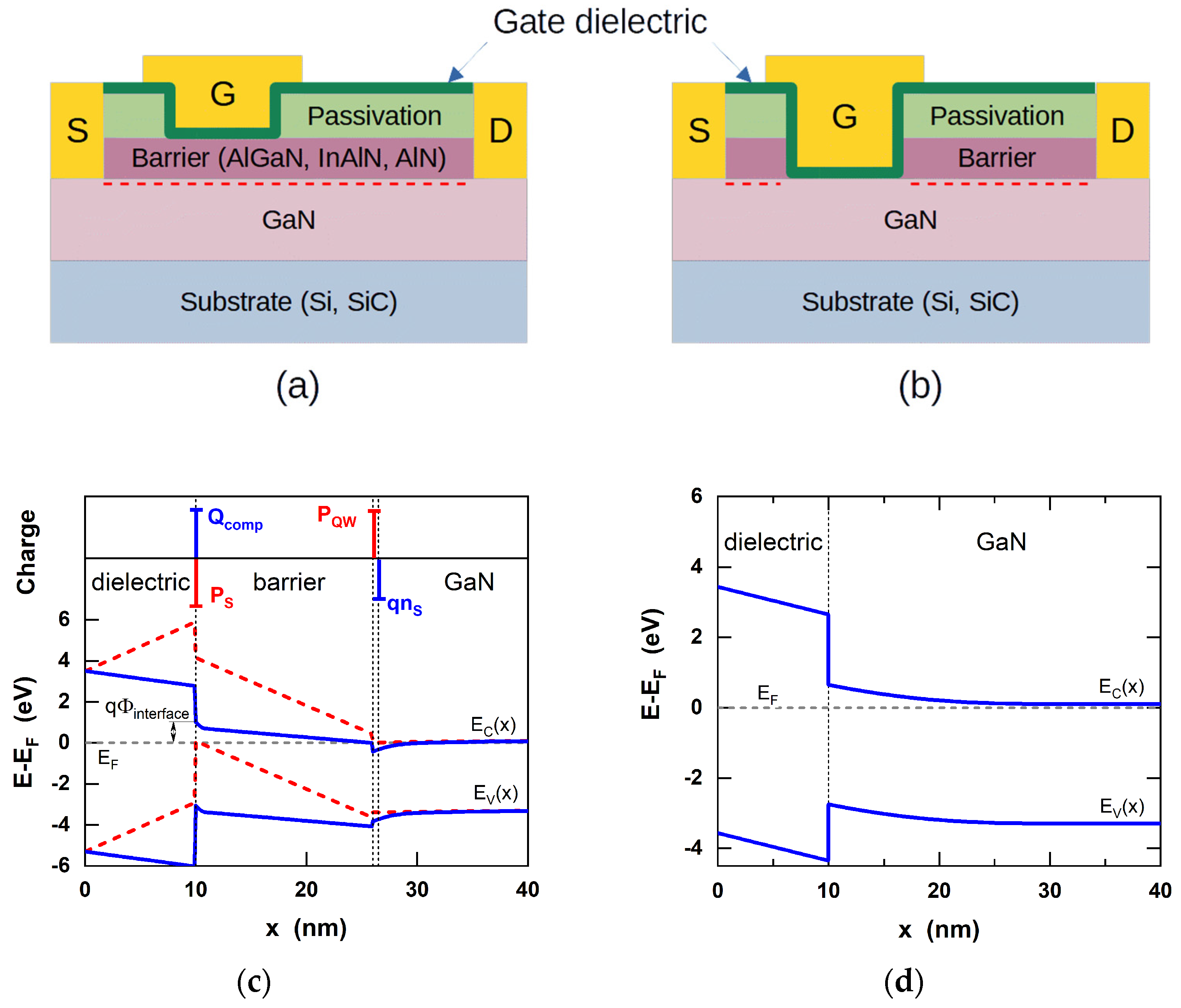
Figure 2.
(a) Schematic illustration of interface traps in Al2O3/AlGaN/GaN MIS heterostructure. (b) Example of two U-shape DIT energy distributions at Al2O3/AlGaN interface used for capacitance–voltage (CV) simulations, highlighting interface traps in the upper part of the bandgap that affect the CV stretch-out. Panel (b) reprinted from [15], with the permission of AIP Publishing. Copyright © 2020 AIP.

Figure 3.
(a) Oxide trap (OT) defect band models in the SiNx/Al2O3 gate dielectric (left) and the energy distribution of the gate dielectric defects for to two different gate dielectrics (right). Copyright © 2020 IEEE. Reprinted, with permission, from Ref. [27]. (b) BT model for the Fermi level pinning due to K-centers inside the silicon nitride. At the Si3N4/(Al)GaN interface, a U-shaped distribution of IT and one discrete donor level (BT). Copyright © 2020 AIP. Reprinted from [34], with permission from AIP.

Figure 4.
(a) Schematic cross-sectional band diagrams of MISHEMT under the gate showing an example of dielectric/barrier interface traps (ITs) and oxide traps (OTs) distributed in the dielectric layer in thermal equilibrium (a) and under positive (b) and negative (c) VG applied and possible capture and emission processes inducing different VTH shifts (b,c).
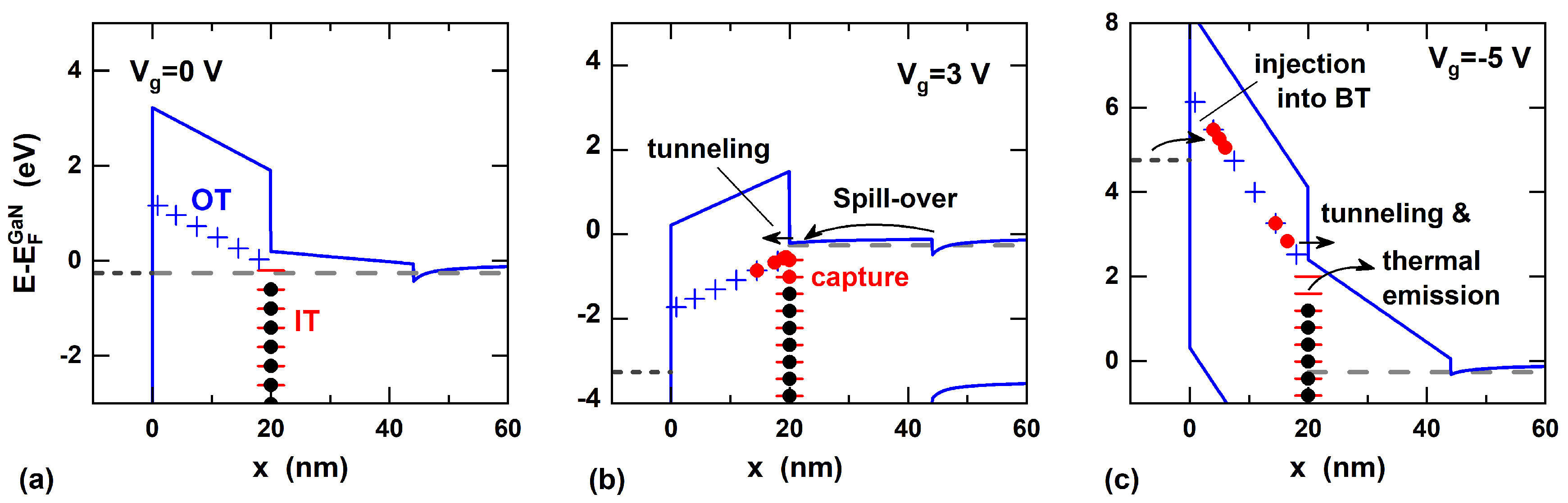
Figure 5.
Example of double-sweep CV characteristic measured on large-area Al2O3/AlGaN/GaN MISHEMT structure together with the “ideal” CV curve, calculated using Poisson solver.
Figure 5.
Example of double-sweep CV characteristic measured on large-area Al2O3/AlGaN/GaN MISHEMT structure together with the “ideal” CV curve, calculated using Poisson solver.
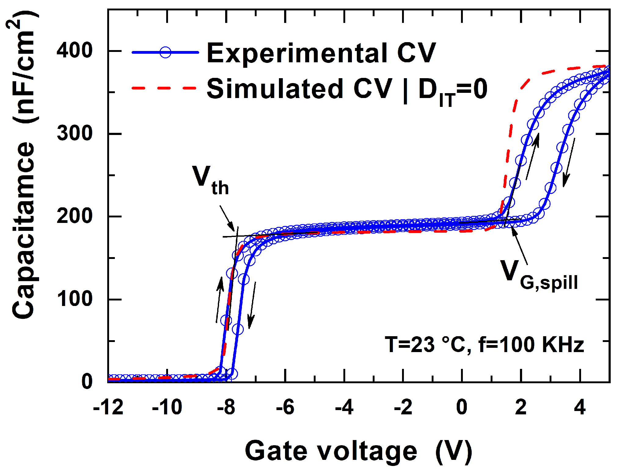
Figure 6.
(a). Band diagrams of MISHEMT structures calculated using Poisson equation and assuming Qinterface/q of −1 × 10¹³ (w/o PDA) and 1 × 1012 cm−2 (w/PDA). Experimental (b) and simulated (c) CV hysteresis of MISHEMT structures without and with PDA measured using different maximum VG ranging from 0 to 7 V. Reprinted from [41], with permission from Elsevier. Copyright © 2020 Elsevier.
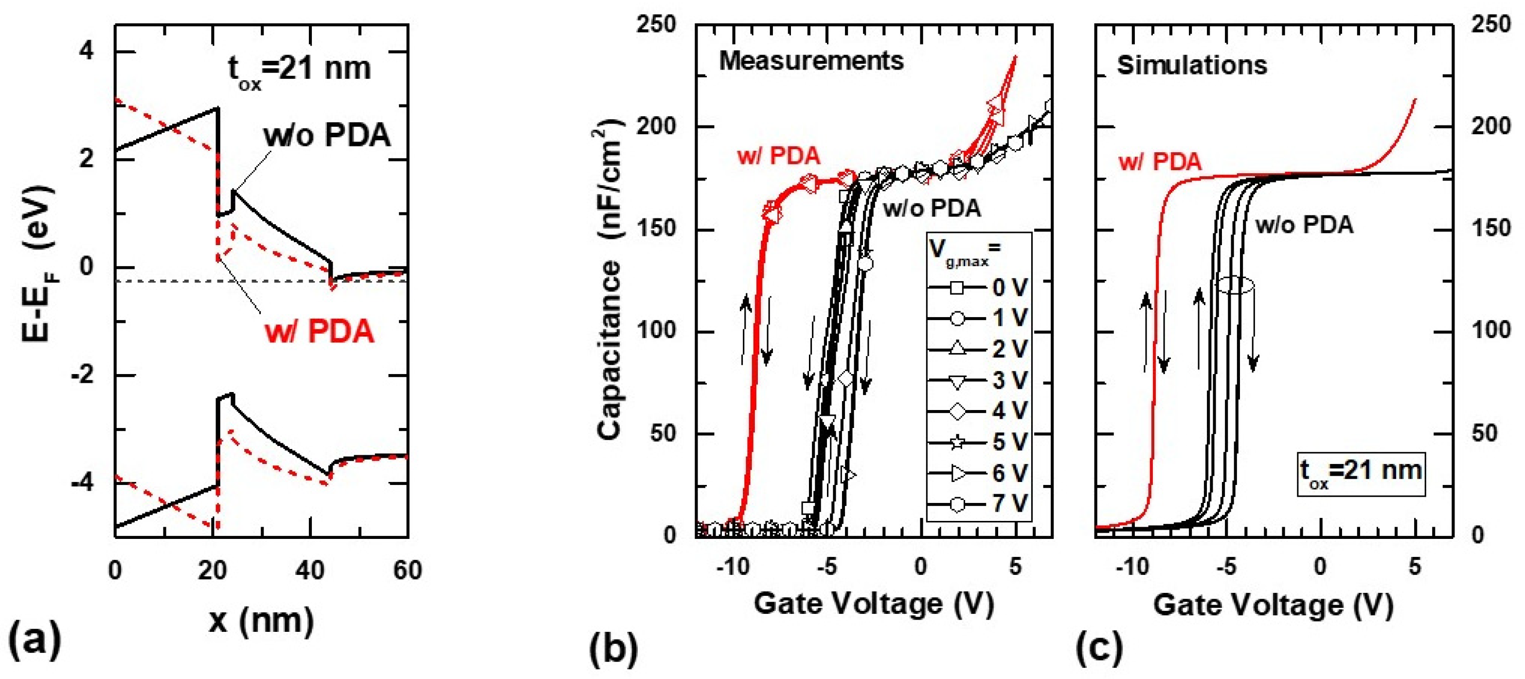
Figure 7.
Measurement setup (a) and pulse pattern (b) used for stress-recovery cycle of measure-stress-measure (MSM) technique. To measure the transient response of VD, the biases are pulsed to VG = VG,meas and VD = VD,meas. (c,d) Example of recovery transients measured for constant VG,stress = 4 V and varying stress times ranging from 100 ns to 100 ks (c) and for constant tstress of 100 s while varying VG,stress from 1 to 7 V (d). Reprinted from Ref. [22], with permission from IEEE. Copyright © 2020 IEEE.
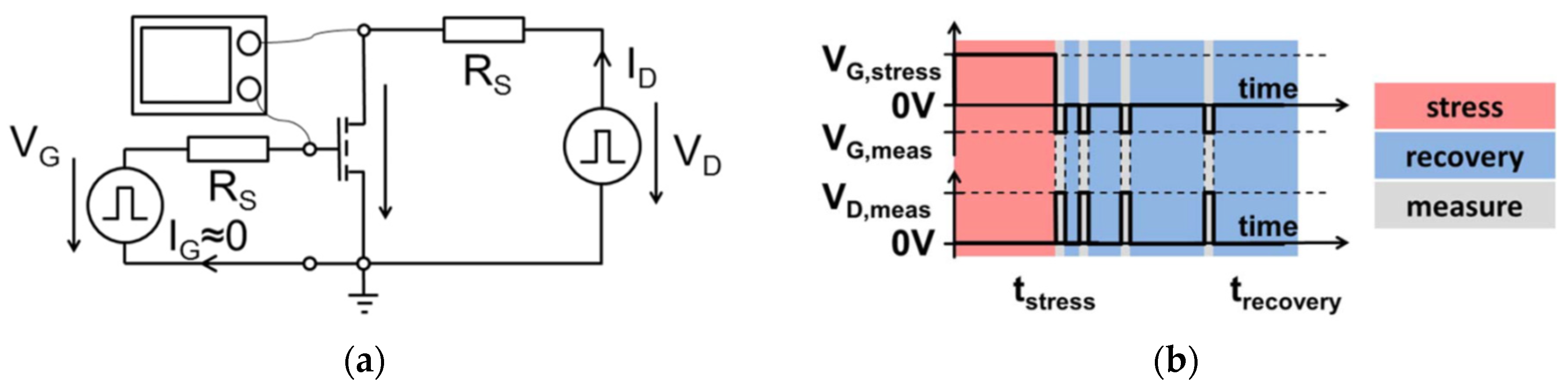
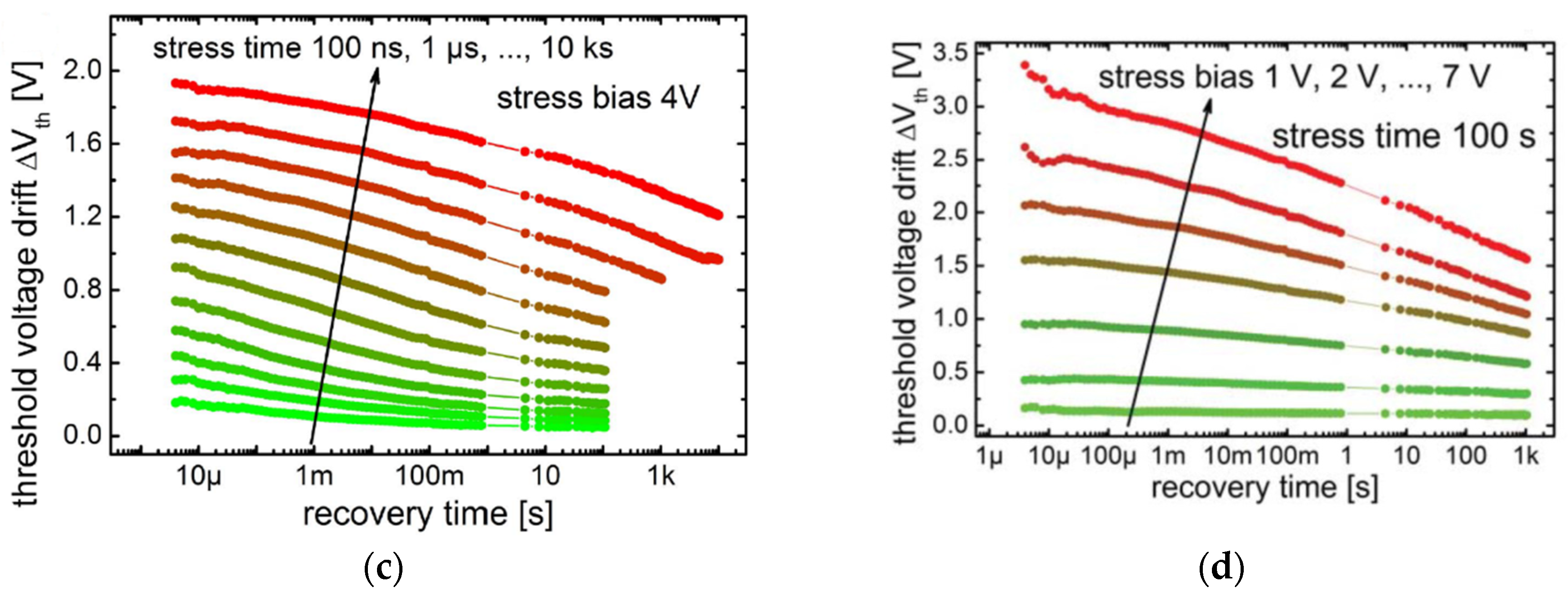
Figure 8.
(a) Capture emission time (CET) map extracted from the recovery transients exemplified in Figure 7 (c,d). © 2020 IEEE. Reprinted, with permission, from Ref. [22]. (b) Measured dependence of ΔNIT on the dielectric charge QD/q. The deviation from linear dependence between the different samples originates from the variation in VG,spill. Reprinted from Ref. [114], with a permission of AIP Publishing. Copyright © 2020 AIP.
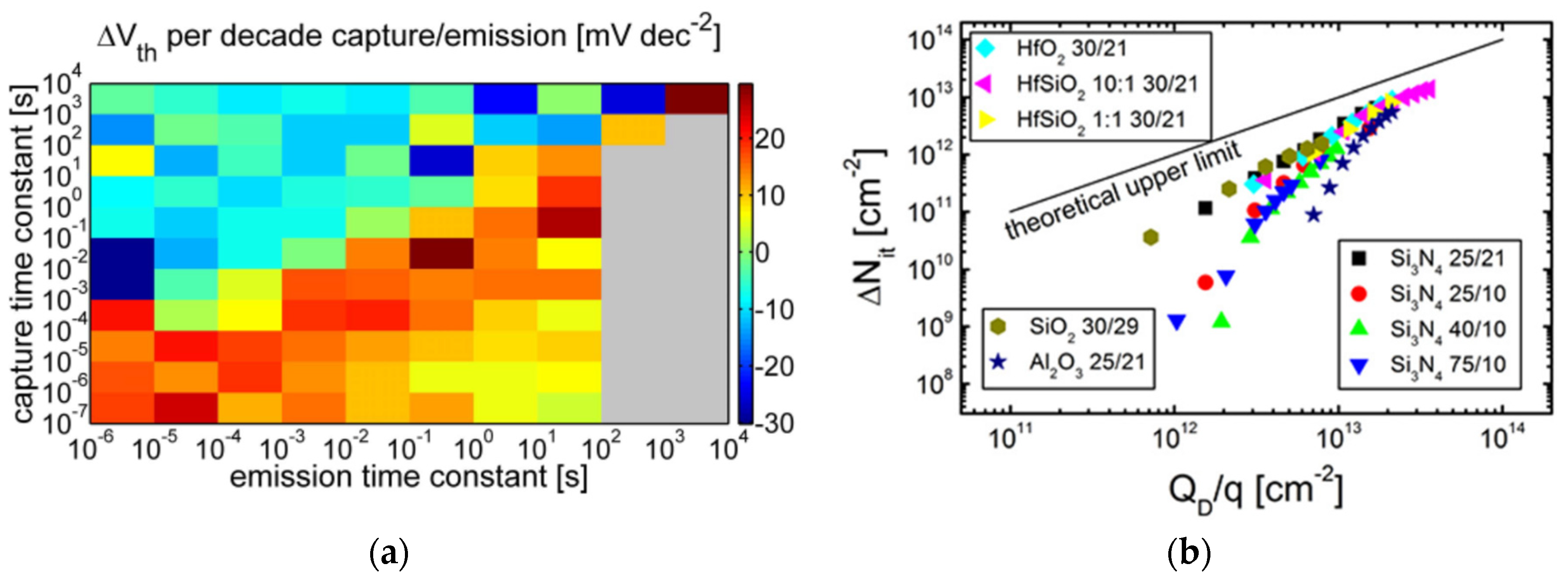
Figure 9.
(a) Successive MSM measurement of Ni/Al2O3/InGaN/AlGaN/GaN MOS HEMT (stress—left, recovery—right). Measurements start with the shortest stressing time (0.1 s) and continue with increased stressing time. (b) Schematic representation of selected processes during stress. Electrons are injected from 2DEG into InGaN. Electrons recombine with holes in InGaN and emit photons that, in turn, de-trap interface states. Emitted electrons from interface states tunnel into conduction band (CB) through triangular barrier. Copyright © 2020 Elsevier. Reprinted, with permission, from Ref. [25].
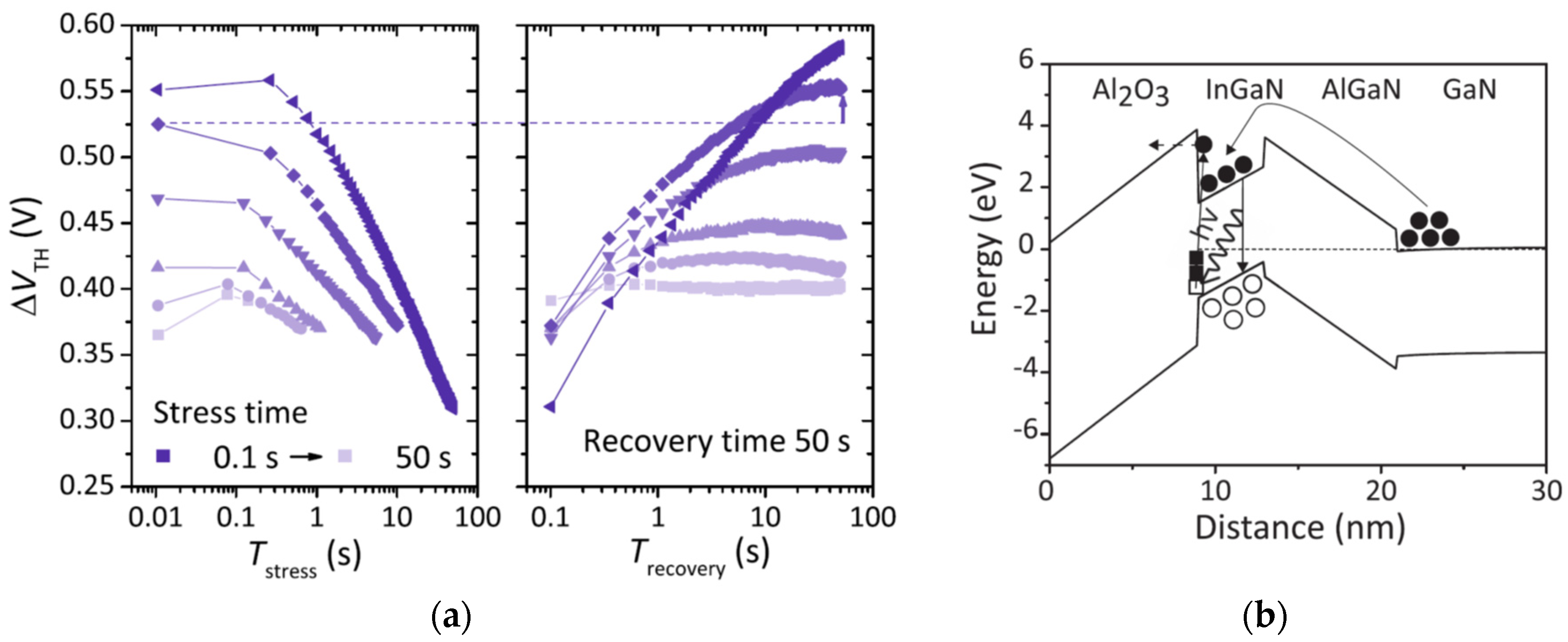
Figure 10.
ΔVTH transients for different tstress of fully-recessed MISFETs with (a) plasma-enhanced ALD (PEALD) SiN and (b) ALD Al2O3 gate dielectric in a logarithmic–logarithmic scale. Dashed lines represent the power-law fits (Equation (6)) to the data. (c) Recovery transients fitted with the universal relaxation model (Equations (7) and (8)) showing faster relaxation for the device with Al2O3 gate dielectric. Copyright © 2020 IEEE. Reprinted, with permission, from Ref. [27].

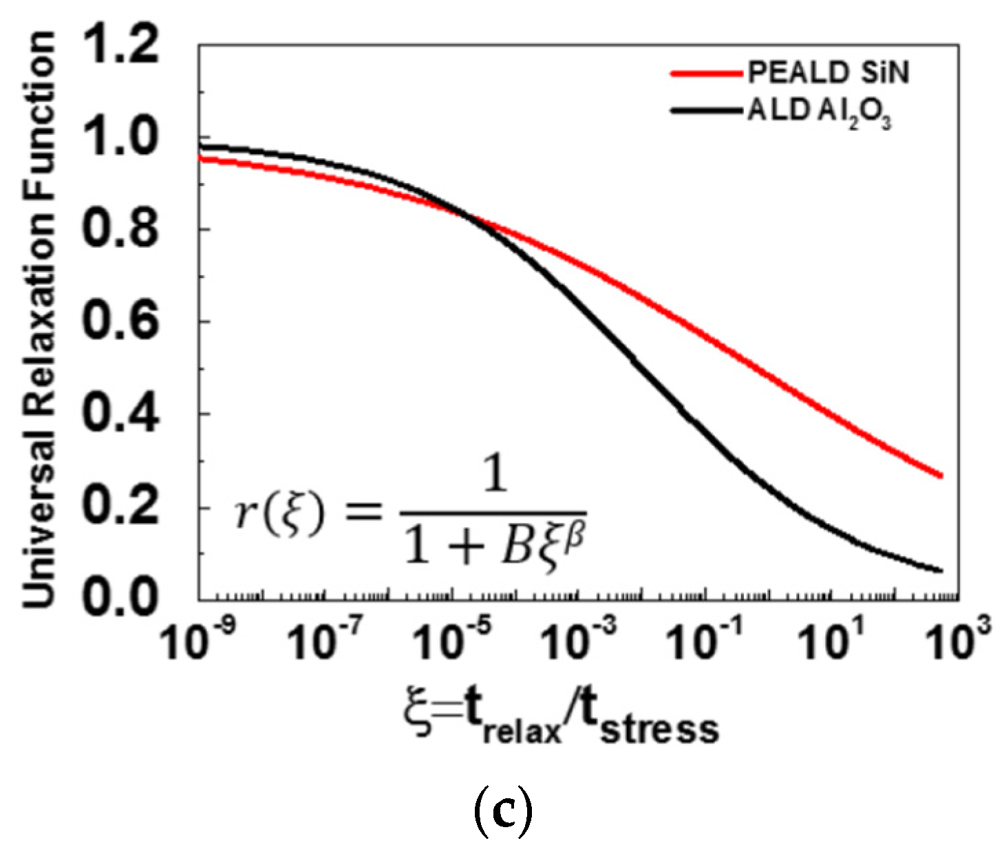
Publisher’s Note: MDPI stays neutral with regard to jurisdictional claims in published maps and institutional affiliations. |
© 2020 by the author. Licensee MDPI, Basel, Switzerland. This article is an open access article distributed under the terms and conditions of the Creative Commons Attribution (CC BY) license (http://creativecommons.org/licenses/by/4.0/).
Share and Cite
MDPI and ACS Style
Ťapajna, M. Current Understanding of Bias-Temperature Instabilities in GaN MIS Transistors for Power Switching Applications. Crystals 2020, 10, 1153. https://doi.org/10.3390/cryst10121153
AMA Style
Ťapajna M. Current Understanding of Bias-Temperature Instabilities in GaN MIS Transistors for Power Switching Applications. Crystals. 2020; 10(12):1153. https://doi.org/10.3390/cryst10121153
Chicago/Turabian StyleŤapajna, Milan. 2020. "Current Understanding of Bias-Temperature Instabilities in GaN MIS Transistors for Power Switching Applications" Crystals 10, no. 12: 1153. https://doi.org/10.3390/cryst10121153
Note that from the first issue of 2016, this journal uses article numbers instead of page numbers. See further details here.