Article

Microstructure and Mechanical Properties of Platinum Fiber Fabricated by Unidirectional Solidification

1
New Industry Creation Hatchery Center (NICHe), Tohoku University 6-6-10, Aoba, Aramaki, Aoba-Ku, Sendai, Miyagi 980-8579, Japan
2
C&A Corporation 1-15-9, Ichiban-cho, Aoba-ku, Sendai, Miyagi 980-0811, Japan
3
Institute for Materials Research, Tohoku University 2-1-1, Katahira, Aoba-Ku, Sendai, Miyagi 980-8577, Japan
*
Author to whom correspondence should be addressed.
Crystals 2020, 10(3), 216; https://doi.org/10.3390/cryst10030216
Submission received: 3 February 2020 / Revised: 11 March 2020 / Accepted: 17 March 2020 / Published: 19 March 2020

Abstract

:
The microstructure and mechanical properties of platinum (Pt) fibers fabricated by unidirectional solidification using the alloy-micro-pulling-down (A-μ-PD) method were investigated using a Universal Testing Machine and Electron Backscattered Diffraction (EBSD). The Pt fiber fabricated at a growth rate of 10 mm/min was composed of relatively large grains with <100> crystal orientation along the growth direction. The crystal orientation was consistent with the easy axis of the crystal growth on the face-centered-cubic (f.c.c.) structure. On the other hand, the adjacent grains of the Pt fiber fabricated at 50 mm/min were randomly oriented owing to a faster growth rate. In tensile tests, the Pt fibers fabricated by the A-μ-PD method indicated extremely different stress–strain curves compared to the commercial Pt wire. The maximum tensile stress of the Pt fiber reached ~100 MPa, and the Pt fiber ruptured after 58% nominal strain.

1. Introduction

Platinum group metals have a high melting point (1830–3300 °C) and relatively high oxidation resistance at high temperatures, and they have been used for various industrial applications such as spark plugs and thermocouples [1]. Generally, products using Pt group metals have been manufactured by various working methods such as sintering, molding, and hammering. However, some Pt group metals and alloys have low workability owing to brittleness, which results in high manufacturing costs and difficulty in controlling the shape. For example, Iridium (Ir) wires can be manufactured by a number of wire-drawing processes using an ingot but Ruthenium (Ru) wires cannot be fabricated by existing methods.
On the other hand, inorganic single crystals have been manufactured by melt-growth approaches such as the Czochralski (Cz) [2,3], Vertical Bridgman (VB) [4,5], and micro-pulling-down (μ-PD) methods [6,7,8,9,10,11,12,13,14]. In particular, the μ-PD method is suitable for the material research of single crystals because it has a faster growth rate than other conventional melt-growth methods [6,7,8,9]. In addition, a shaped single crystal can be synthesized directly from the melt by controlling the shape of the solid-liquid interface during crystal growth [10,11,12,13,14].
Recently, we developed an alloy-μ-PD (A-μ-PD) method for the growth of metal and alloy fibers with precise shape control [15]. In a previous paper, Pt fibers of approximately 1 mm in diameter were fabricated from the melt by the A-μ-PD method [16]. The Pt fiber was composed of relatively large grains originating from the melt-growth by unidirectional solidification. There is a high possibility of different mechanical properties for Pt fiber fabricated by the A-μ-PD method (Pt fiberA-μ-PD) compared to commercial Pt wire produced by the conventional wire-drawing process (WDP) (Pt wireWDP).
In this paper, we investigated the microstructures and mechanical properties of Pt fiberA-μ-PD fabricated at various growth rates using Scanning Electron Microscopy–Electron Backscattered Diffraction (SEM–EBSD) and a Universal Testing Machine Autograph, respectively. In addition, the results of the microstructures and mechanical properties were compared with those of Pt wireWDP to reveal the industrial value of the Pt fiberA-μ-PD.

2. Experimental

Pt fibers with a diameter of 0.95 mm were fabricated from the melt by the A-μ-PD method at various growth rates. The lengths of the Pt fibers fabricated with growth rates of 10 and 50 mm/min were 5 m and 100 mm, respectively. Other growth conditions and states during the fiber fabrication were described in a previous report [16]. In addition, a commercial-use Pt wire with a diameter of 1.00 mm manufactured by the wire-drawing process (Tanaka Kikinzoku Kogyo Corp.) was prepared for comparison with the Pt fiberA-μ-PD.
The Pt fibers and Pt wireWDP were cut perpendicular to the growth and longitudinal directions, respectively, and specimens approximately 5 mm in length were prepared for measuring the microstructure and mechanical properties. The specimens were mechanically polished along the growth and longitudinal directions. Damaged layers on the polished surface were removed by an Ar+ ion beam using a cross-section polisher (CP) (JEOL, Tokyo, Japan, IB-09020CP) to observe the microstructure and crystal orientation.
Microstructures on the CP-treated surfaces of the polished specimens were observed by SEM, and their inverse pole figures (IPF) were evaluated by SEM–EBSD (JEOL, Tokyo, Japan, JSM-7800F) to identify the crystal orientation of each domain. Tensile tests were conducted on the Pt fiberA-μ-PD and the Pt wireWDP by a Universal Testing Machine Autograph (Shimadzu, Kyoto, Japan, AG-10 kN). Specimens of 40 mm in length for the tensile test were prepared from the Pt fiberA-μ-PD and the Pt wireWDP. The tensile tests were carried out at strain rates of 1.1 × 10⁻³ and 1.1 × 10⁻⁵ s−1 at room temperature (25 °C). The nominal stress and strain were calculated from the force applied to a load cell and stretching distance at a fractured point under stretching. After the tensile tests, surfaces at the fractured points were observed by SEM.

3. Results and Discussion
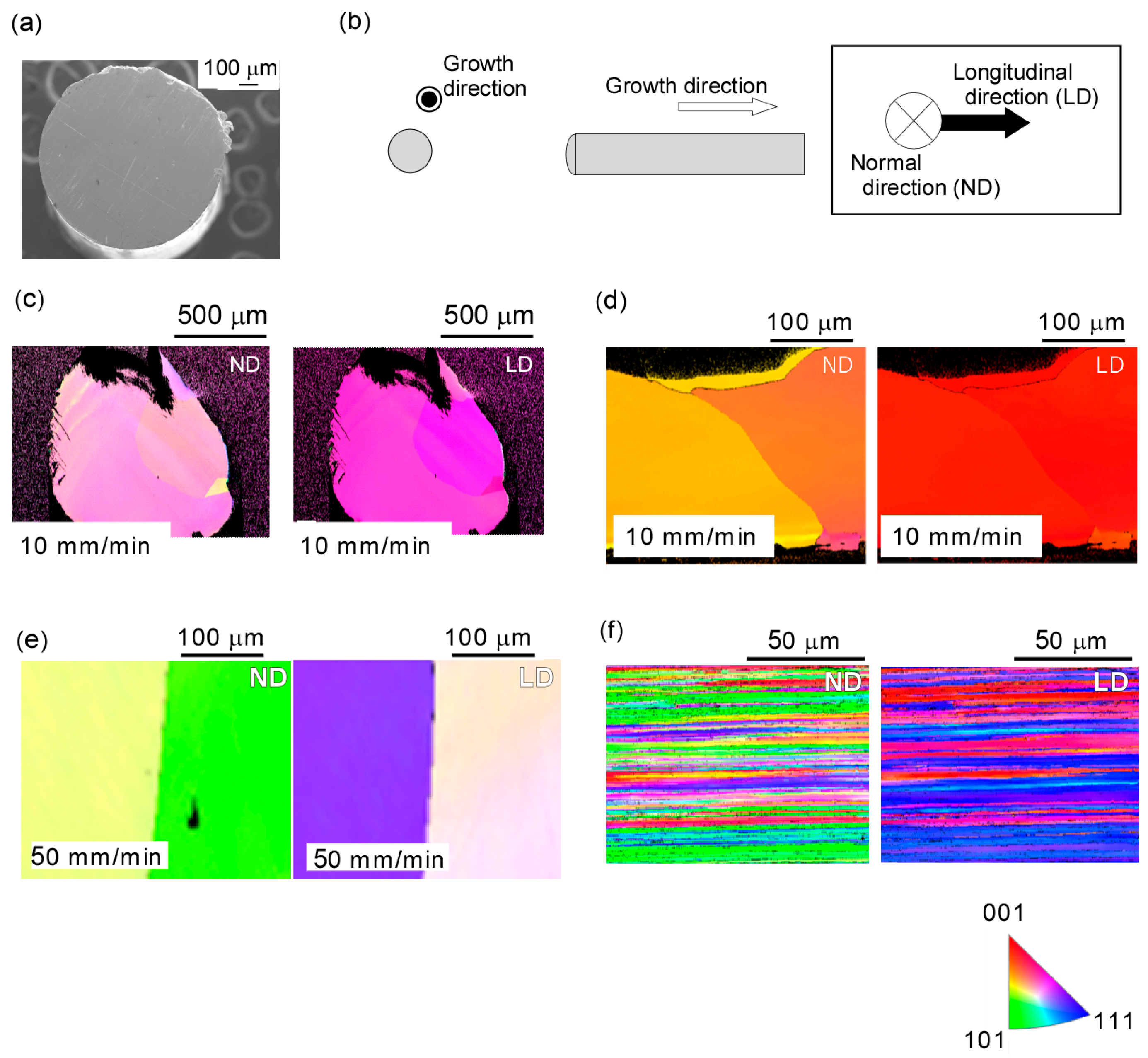
3.1. Microstructure

Figure 1a shows an SEM image on the cross-sectional plane of the Pt fiber fabricated at a 10-mm/min growth rate. The cross-sectional plane showed a precise circle, and the cross-sectional area was 0.702 mm2. The CP-treated surface of the Pt fibers was analyzed by SEM–EBSD to clarify the internal grain structures. Figure 1b shows a schematic diagram of the relationship between the specimens and each direction. Figure 1c–f shows IPF maps of the polished surfaces of the Pt fiberA-μ-PD and the Pt wireWDP. Colors in the IPF maps represent the crystal orientation of each domain in the longitudinal direction (LD) and normal direction (ND).
The LD of the Pt fiberA-μ-PD is the growth direction, and the LD of the Pt wireWDP is the wire-drawing direction. Figure 1c,d shows IPF maps of the crystal orientations of the ND and LD on the CP-treated surfaces perpendicular and parallel to the growth direction for the Pt fiber fabricated at a 10-mm/min growth rate, respectively. There were three grains in Figure 1c, and a grain boundary perpendicular to the LD (growth direction) was observed in the center of Figure 1d. A grain boundary perpendicular to the LD was also observed in the IPF maps of the Pt fiber fabricated at a 50-mm/min growth rate, as shown in Figure 1e. Both Pt fiberA-μ-PD fabricated at 10- and 50-mm/min growth rates were composed of relatively large grains with a diameter of more than 1 mm. On the other hand, the Pt wireWDP was composed of many small grains with high aspect ratios, and elongated grains were aligned along the LD, as shown in Figure 1f. The thicknesses of the elongated grains were 2–10 μm, and the lengths were greater than 100 μm, revealing that the microstructure of the Pt fiberA-μ-PD is very different from that of the Pt wireWDP.
According to an evaluation of crystal orientations by EBSD, the adjacent grains of the Pt fiberA-μ-PD fabricated at a 10-mm/min growth rate showed the same crystal orientation of the <100> direction in the LD, while the crystal orientations between the grains were slightly different in the ND (Figure 1d). The <100> direction is consistent with the easy axis of crystal growth on the face-centered-cubic (f.c.c.) structure of Pt. On the other hand, the crystal orientations were different between the adjacent grains on the Pt fiberA-μ-PD fabricated at a 50-mm/min growth rate, and the grains were randomly oriented (Figure 1e). The results suggest that the grains were relaxed to minimize the thermal stress at a 50-mm/min growth rate compared to a 10-mm/min growth rate. As a result, the grains were textured by selecting the best orientation to minimize thermal stress.

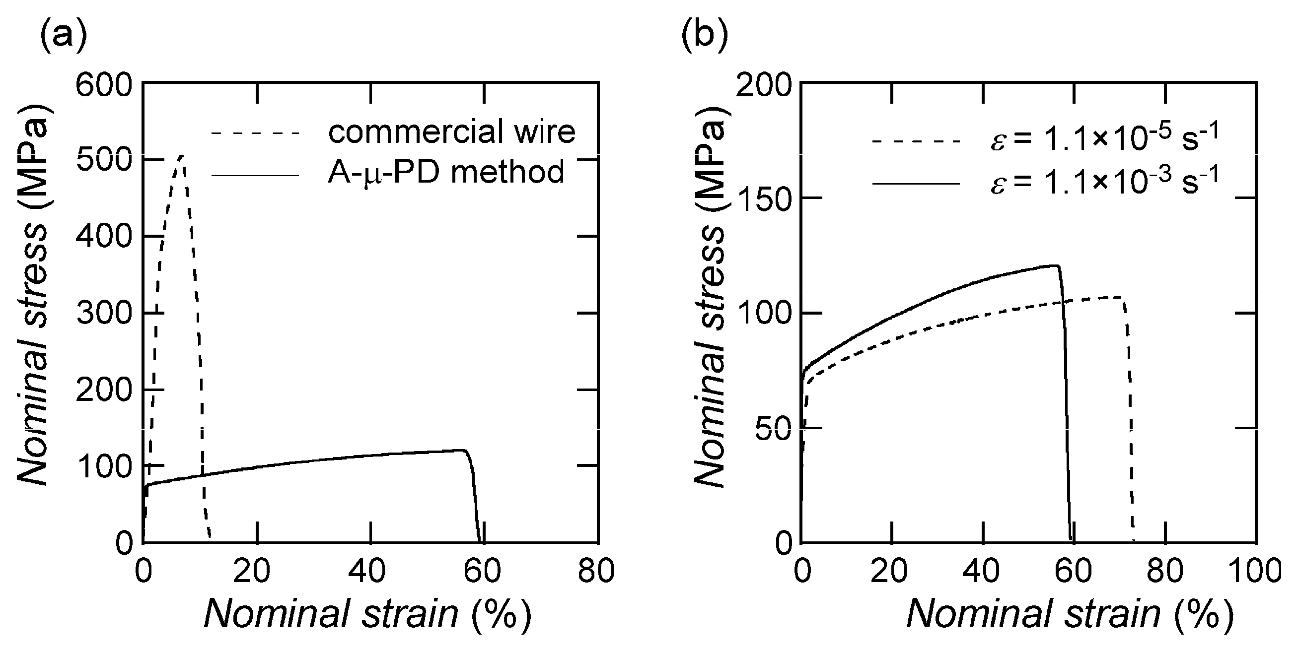
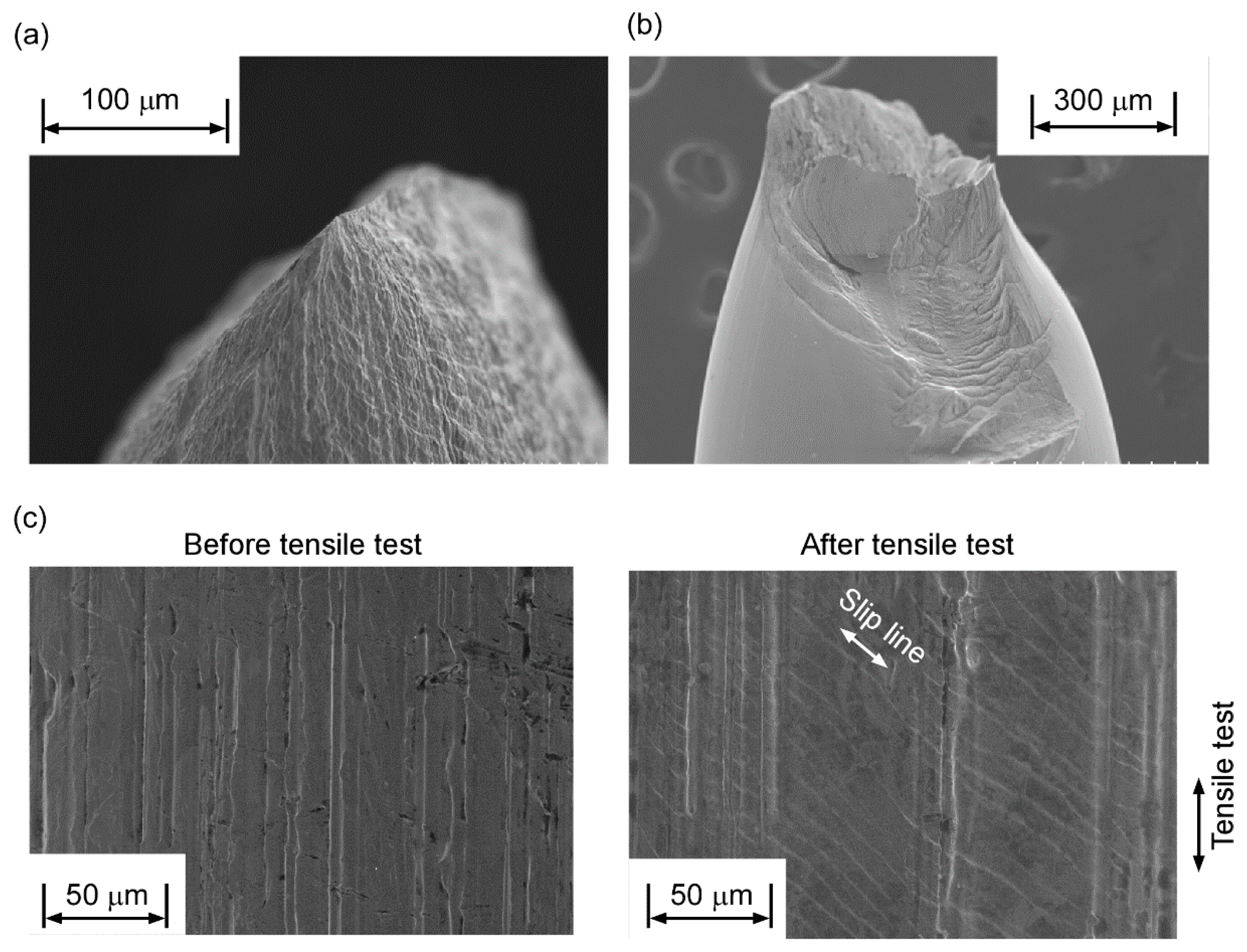
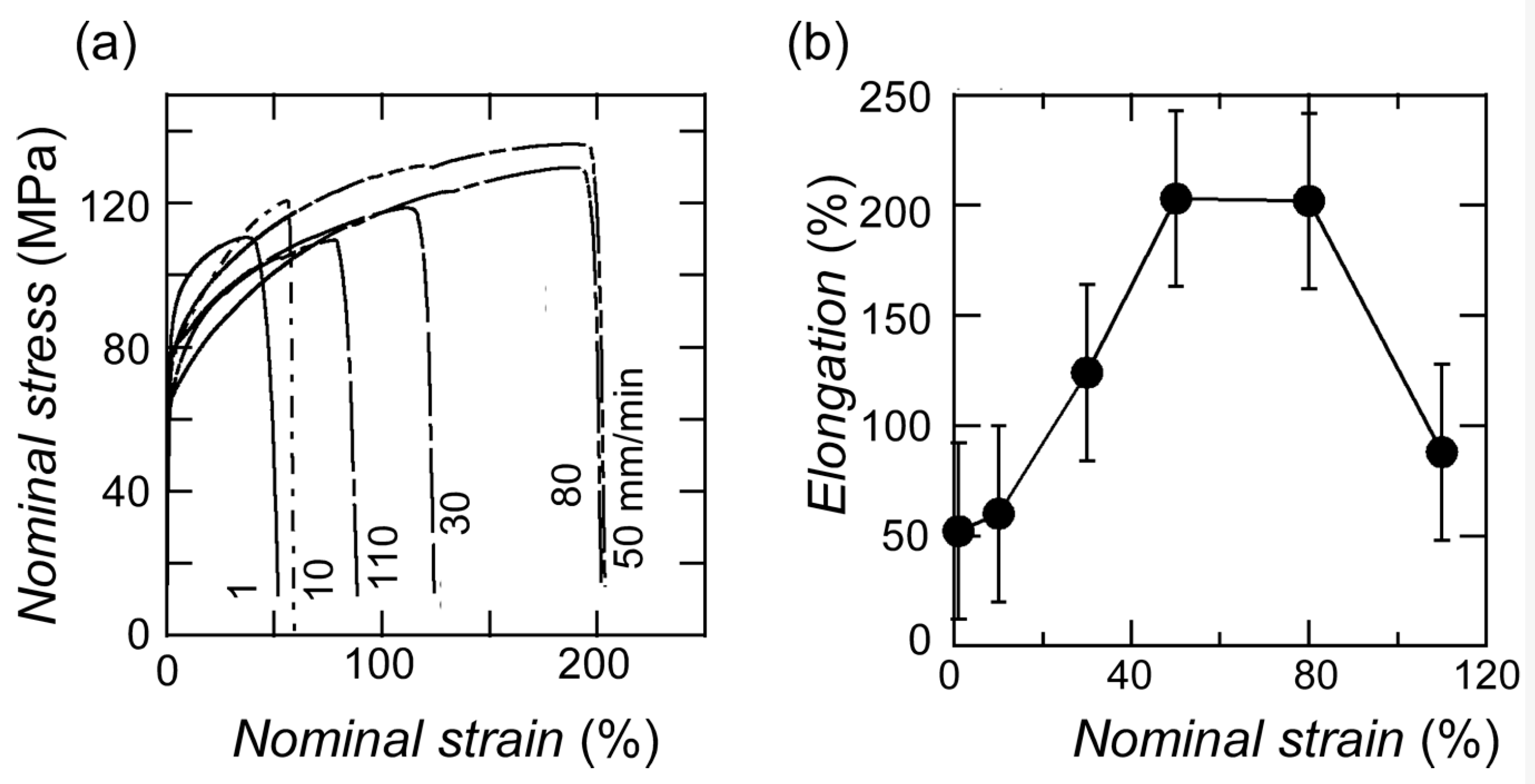
3.2. Mechanical Properties

Typical stress–strain curves of the Pt fiberA-μ-PD and the Pt wireWDP were measured, as illustrated in Figure 2. Figure 2a shows the stress–strain curves of the Pt fiber fabricated at a 10-mm/min growth rate and the Pt wireWDP. The nominal stress of the Pt wireWDP gradually increased as the nominal strain increased to the maximum point, and then it gradually decreased. At the maximum point, the nominal stress of the Pt wireWDP reached ~500 MPa, and the elongation at the point was ~10%.
On the other hand, the nominal stress of the Pt fiberA-μ-PD fabricated at 10 mm/min steeply increased as the nominal strain increased to ~65 MPa, similar to the Pt wireWDP, and it is the elastic deformation region. After the elastic deformation region, the nominal stress gradually increased with a shallow slope in the nominal strain range of 0.5–58%. After the Pt fiber was elongated by more than 22%, the nominal strain reached ~100 MPa. Then, the Pt fiberA-μ-PD ruptured at 58% nominal strain. The results suggest that the differences in the stress–strain curves between the Pt fiberA-μ-PD and the Pt wireWDP are attributable to the differences between the grain structures. Figure 2b shows the stress–strain curves of Pt fibers fabricated at a 10-mm/min growth rate with different strain rates. The elongation value and maximum tensile strength decreased as the strain rate increased.
The surfaces at the fractured points of the Pt fiberA-μ-PD and the Pt wireWDP were observed by SEM after the tensile tests, as shown in Figure 3. Only an edge without the fracture surface was observed at the fractured point of the Pt fiberA-μ-PD, and it is a chisel-type edge (Figure 3a). On the other hand, there was a fracture surface at the fractured point of the Pt wireWDP, and dimples were observed on the fracture surface (Figure 3b). Figure 3c shows the side surface of the Pt fiberA-μ-PD fabricated at a 10-mm/min growth rate at several millimeters from the fractured point. A large number of sliding faces were uniformly generated in the Pt fiberA-μ-PD along the inclined direction to the longitudinal direction (white lines in Figure 3c). According to the positional relationship between the <100> growth direction of the Pt fiber and the close-packed {111} plane, it is considered that sliding occurred along the {111} plane. On the other hand, the difference of the side surface of the Pt wireWDP could not be observed before and after the tensile test.
Figure 4a shows the stress–strain curves of the Pt fiberA-μ-PD fabricated at various growth rates (10–110 mm/min). The stress–strain curves for all specimens showed similar tendencies, and the maximum strengths were approximately 100 MPa regardless of the growth rate. On the other hand, the elongations at breaking obtained from the stress–strain curves were changed by the growth rate. The growth rate dependence of the breaking elongation is shown in Figure 4b. The breaking elongation gradually increased as the growth rate increased, and reached the maximum value at a 50–80-mm/min growth rate. After the maximum value, the breaking elongation decreased at a 110-mm/min growth rate.
The results suggest that the differences in the breaking elongations of the Pt fiberA-μ-PD fabricated at various growth rates are attributable to the direction of the {111} sliding plane in the tensile direction. On the other hand, the fabrication of the Pt fiber became unstable around a 110-mm/min growth rate [16], and the elongation dropped at a 100-mm/min growth rate, a phenomenon that originated from the nonuniform diameter of the Pt fiber.

4. Conclusions

Pt fiberA-μ-PD and Pt wireWDP were evaluated by SEM–EBSD and a Universal Testing Machine to reveal the microstructure and physical properties. Grains in the Pt fiber fabricated at 10-mm/min growth rate were aligned in the <100> direction along the growth direction, while the crystal orientations of the grains in the Pt fiber fabricated at 50 mm/min were random. In tensile tests of the Pt fibers, the maximum value of the tensile strength was ~100 MPa, and the breaking elongation was more than 50%. The results revealed that the Pt fiberA-μ-PD had a large tensile ductility in contrast to the Pt wireWDP wire made by the wire-drawing process. We were able to control the microstructure and physical properties by the growth rate.

Author Contributions

Conceptualization, Y.Y.; investigation, Y.Y. and T.N.; resources, T.N.; data curation, T.N.; writing—original draft preparation, Y.Y.; writing—review and editing, Y.Y.; visualization, Y.Y. and T.N.; supervision, Y.Y., M.Y., A.Y., S.T., H.S., Y.O., S.K., K.K. and A.Y.; project administration, Y.Y. and A.Y.; funding acquisition, Y.Y. All authors have read and agreed to the published version of the manuscript.

Funding

This research was funded by the New Energy and Industrial Technology Development Organization (NEDO), grant number 18100496-0, and Japan Society for the Promotion of Science (JSAP), Grant-in-Aid for Young Scientists (A), grant number 15H05551. In addition, this research was also funded by the Intelligent Cosmos Academic Foundation.

Acknowledgments

We thank Magara for technical assistance with the cross-section polisher treatment and SEM–EBSD analysis at the Tohoku University Material Solutions Center (MaSC).

Conflicts of Interest

The authors declare no conflict of interest.

References

  1. Hamada, T.; Hitomi, S.; Ikematsu, Y.; Nasu, S. High-temperature creep of pure platinum. Mater. Trans. JIM 1996, 37, 353–358. [Google Scholar] [CrossRef] [Green Version]
  2. Kamada, K.; Shoji, Y.; Kochurikhin, V.V.; Okumura, S.; Yamamoto, S.; Nagura, A.; Yeom, J.Y.; Kurosawa, S.; Yokota, Y.; Yoshikawa, A. Growth and scintillation properties of 3 in. diameter Ce doped Gd3Ga3Al2O12 scintillation single crystal. J. Cryst. Growth 2016, 452, 81–84. [Google Scholar] [CrossRef] [Green Version]
  3. Yokota, Y.; Kudo, T.; Ohashi, Y.; Medvedev, A.; Kurosawa, S.; Kamada, K.; Yoshikawa, A. Growth and piezoelectric properties of Ca3Nb(Ga1-xAlx)3Si2O14 (x = 0.25 and 0.50) single crystals. Jpn. J. Appl. Phys. 2015, 54, 10ND13. [Google Scholar] [CrossRef]
  4. Yokota, Y.; Ito, T.; Shoji, Y.; Kurosawa, S.; Ohashi, Y.; Kamada, K.; Yoshikawa, A. Growth of 1.5-In Eu:SrI2 Single Crystal and Scintillation Properties. IEEE Trans. Nucl. Sci. 2015, 63, 467–470. [Google Scholar] [CrossRef]
  5. Yoshikawa, A.; Shoji, Y.; Yokota, Y.; Kurosawa, S.; Hayasaka, S.; Chani, V.; Ito, T.; Kamada, K.; Ohashi, Y.; Kochurikhin, V. Growth of 2 inch Eu-doped SrI2 single crystals for scintillator applications. J. Cryst. Growth 2016, 452, 73–80. [Google Scholar] [CrossRef] [Green Version]
  6. Yoshikawa, A.; Nikl, M.; Boulon, G.; Fukuda, T. Challenge and study for developing of novel single crystalline optical materials using micro-pulling-down method. Opt. Mater. 2007, 30, 6–10. [Google Scholar] [CrossRef]
  7. Yokota, Y.; Fujimoto, Y.; Yanagida, T.; Takahashi, H.; Yonetani, M.; Hayashi, K.; Park, I.; Kawaguchi, N.; Fukuda, K.; Yamaji, A.; et al. Crystal growth of Na co-doped Ce:LiCaAlF6 single crystals and their optical, scintillation and physical properties. Cryst. Growth Des. 2011, 11, 4775–4779. [Google Scholar] [CrossRef]
  8. Yoshikawa, A.; Chani, V. Growth of optical crystals by the micro-pulling-down method. Mater. Res. Bull. 2009, 34, 266–270. [Google Scholar] [CrossRef]
  9. Yokota, Y.; Kurosawa, S.; Shoji, Y.; Ohashi, Y.; Kamada, K.; Yoshikawa, A. Development of novel growth methods for halide single crystals. Opt. Mater. 2017, 65, 46–51. [Google Scholar] [CrossRef]
  10. Yokota, Y.; Chani, V.; Sato, M.; Tota, K.; Onodera, K.; Yanagida, T.; Yoshikawa, A. Growth and crystallinity of shaped and multiple sapphire crystals by a micro-pulling-down method. J. Cryst. Growth 2011, 318, 983–986. [Google Scholar] [CrossRef]
  11. Yokota, Y.; Yoshikawa, A.; Futami, Y.; Sato, M.; Tota, K.; Onodera, K.; Yanagida, T. Shaped crystal growth of langasite-type piezoelectric single crystals and their physical properties. IEEE Trans. Ultrason. Ferroelectr. Freq. Control 2012, 59, 1868–1871. [Google Scholar] [CrossRef] [PubMed]
  12. Chani, V.; Yoshikawa, A.; Kuwano, Y.; Hasegawa, K.; Fukuda, T. Growth of Y3Al5O12:Nd fiber crystals by micro-pulling-down technique. J. Cryst. Growth 1999, 204, 155–162. [Google Scholar] [CrossRef]
  13. Sato, H.; Chani, V.; Yoshikawa, A.; Kagamitani, Y.; Machida, H.; Fukuda, T. Micro-pulling-down growth and characterization of Tb3-xTmxAl5O12 fiber crystals for Faraday rotator applications. J. Cryst. Growth 2004, 264, 253–259. [Google Scholar] [CrossRef]
  14. Zhuravleva, M.; Chani, V.; Yanagida, T.; Yoshikawa, A. The micro-pulling-down growth of Bi4Si3O12 (BSO) and Bi4Ge3O12 (BGO) fiber crystals and their scintillation efficiency. J. Cryst. Growth 2008, 310, 2152–2156. [Google Scholar] [CrossRef]
  15. Yokota, Y.; Nihei, T.; Ohashi, Y.; Kurosawa, S.; Kamada, K.; Yoshikawa, A. Fabrication of Metallic Fibers with High Melting Point and Poor Workability by Unidirectional Solidification. Adv. Eng. Mater. 2018, 20, 1700506. [Google Scholar] [CrossRef]
  16. Nihei, T.; Yokota, Y.; Arakawa, M.; Ohashi, Y.; Kurosawa, S.; Kamada, K.; Chani, V.; Yoshikawa, A. Growth of platinum fibers using the micro-pulling-down method. J. Cryst. Growth 2016, 468, 403–406. [Google Scholar] [CrossRef]
Figure 1. (a) SEM image of cross-sectional plane for Pt fiberA-μ-PD at 10-mm/min growth rate. (b) Schematic diagram of the relationship between specimens and each direction of SEM–EBSD analysis. IPF maps of Pt fiberA-μ-PD; (c) Perpendicular to growth direction fabricated at 10-mm/min growth rate, and parallel to growth direction fabricated at (d) 10-mm/min and (e) 50-mm/min growth rates. (f) Longitudinal direction of Pt wireWDP.
Crystals 10 00216 g001
Figure 2. (a) Stress–strain curves of Pt fiberA-μ-PD at 10-mm/min growth rate (solid line) and Pt wireWDP (dashed line) at a strain rate of 1.1 × 10⁻³ s−1. (b) Stress–strain curves of Pt fiberA-μ-PD fabricated at 10-mm/min growth rate at strain rates of 1.1 × 10⁻³ and 1.1 × 10⁻⁵ s−1.
Crystals 10 00216 g002
Figure 3. SEM images at fractured points of (a) Pt fiberA-μ-PD at 10 mm/min and (b) Pt wireWDP. (c) SEM images of side surfaces around the fractured point of Pt fibers fabricated at 10-mm/min growth rate at several millimeters from the fractured point before and after the tensile test.
Crystals 10 00216 g003
Figure 4. (a) Stress–strain curves of Pt fiberA-μ-PD at various growth rates. (b) Growth rate dependence of breaking elongation for Pt fiberA-μ-PD.
Crystals 10 00216 g004

