3.1. Pulsed Plating
Figure 3 shows the SEM images, which exhibited uniform, straight, and ultralong Cu NWs. The Cu NWs were synthesized following our previously reported methods [
12] with dimensions of D = 52.1 ± 6.6 nm and L ≥ 100 μm to give high aspect ratio NWs, i.e., length/diameter (L/D) > 2380. Transparent electrodes that were prepared using our Cu NWs demonstrated excellent optoelectronic performance, specifically in terms of sheet resistance (R
s) versus transmittance (%T): 7.3, 30, 58, and 100 Ω/sq at 72.4, 90, 94, and 97% respectively. These results are equivalent to, or even greater than, those of some transparent electrodes based on Cu nanofiber webs (50 Ω/sq at 90%) [
15] and Cu NWs synthesized via the solution route (90 Ω/sq at 90%) [
16].
The result of pulsed nickel electroplating is shown in
Figure 4. The PC plating process successfully deposited nickel onto the Cu NWs. The SEM images in
Figure 4a,b show Cu NWs before and after nickel PC plating, respectively. The diameter of the wires increased from 52.1 ± 6.6 nm to 77.1 ± 6.5 nm due to the deposition of nickel on the wires. This increase in diameter is a major contributor to the increase in light scattering and light absorption, which is probably responsible for the decline in transparency of the electrodes. On the other hand, as illustrated in the schematic in
Figure 4c, after being plated, it appears that the nickel completely covered the NWs and junctions. The nickel atoms deposited at the intersection of two crossing wires would play a vital role in affecting the stability of the Cu NWs. This strengthened link created a solid network and significantly improved conductivity.
As shown in
Figure 5a, energy-dispersive X-ray spectroscopy (EDS) images at a scale of 500 nm showed that the Cu and Ni elements on the sample are extracted from the Cu–Ni electrode after plating by PC. The green line of the Ni element coincided with the violet line of the Cu element, demonstrating that the Ni particles only deposited on the copper wires. Moreover, this is confirmed by the TEM images in
Figure 5b of one Cu nanowire after PC plating at a 100 nm scale. The inset shows the Ni shell and Cu core and clearly demonstrates that the Cu nanowires are completely covered by Ni. The outer Ni layer protects the Cu NW by preventing direct contact with the oxygen in the air, hence reducing the rate of oxidation for several days which will be shown subsequently.
3.2. Influence of Frequency and Duty Cycle on Nickel Deposition
The original Cu NWs (
Figure 6a) had diameters of 52.1 ± 6.6 nm.
Figure 6b−e shows the SEM images of nickel-pulsed electrodeposits under supplied power generated of 0−3 V; the duty cycle was 50%, the plating time was kept constant at 90 s, and the frequencies were 50 Hz, 100 Hz, 200 Hz, and 800 Hz.
Figure 6e indicates the diameters of the Ni-coated Cu NWs as measured by ImageJ, and the crystallite size (grain size) was determined using the Scherrer equation utilizing the peak broadening of the (111) diffraction peak:
The SEM images presented above demonstrate that the Ni coating layer was more rugged when plated at low frequency. From
Figure 6e, it can be noted that increasing the frequency results in an increase in the crystallite size but a decline in the diameter. In order to explain the influence of frequency, by expressing the nucleation rate through current
I, the relationship between three-dimensional nucleation rate and the overpotential is illustrated in the formula below [
17]:
where
A and
B are constant, and
η is the overpotential. Following this relation, as the overpotential increases, the speed of new crystal nucleus creation will also increase leading to a decrease in the crystallite size. If a certain quantity of new grains is formed rapidly, then more compact delicate deposits are obtained. When the frequency increases from 50 Hz to 800 Hz, it means that both T
on and T
off decrease in a cycle. Our experiments agree with previous results as mentioned by Yuan [
17], in which he found that as the T
on in a cycle fell, the overpotential also fell and the crystallite size of the deposits increased.
XRD patterns were chosen to investigate the effect of duty cycle (
ϕ) on nickel deposition. As shown in
Figure 7, with an increase in the duty cycle from 33% to 67%, the (111) texture was still the preferred orientation of the deposits.
Generally, transparent electrodes for industrial applications must exhibit acceptable uniformity. Practically, however, due to the effect of current distribution, it is very difficult to create a 100% uniform layer via the electroplating technique [
18]. This study found that an even distribution can be achieved by selecting a suitable combination of frequency (
f) and duty cycle (
ϕ). These two factors are crucial for optimizing the electroplating process. To determine the optimum values, three criteria are considered:
(1) The difference of transmittances: ΔT = Tafter − Tbefore, (at a wavelength of 550 nm) of the Cu NW electrodes before and after plating.
(2) The difference of sheet resistances: ΔR = Rafter − Rbefore of the Cu NW electrodes before and after plating.
(3) The uniformity of the electrodes after plating, which can be evaluated by observing and measuring the transparency at different positions on the Cu–Ni NW electrodes.
In an attempt to optimize the frequency and duty cycle (
ϕ) in the plating process, fifteen Cu NW electrodes with an original transparency of 83% and sheet resistance of 20 Ω/sq were prepared. These samples were plated for 90 s under supplied power generated with a pulse of 0 V–3 V. A range of frequencies from 50 to 800 Hz and 3 different duty cycles (
ϕ) of 33.3%, 50%, and 66.7% were investigated.
Figure 8a shows the difference in sheet resistance before and after pulsed electrodeposition of Ni; all the electrodes were conductive, proving that the wires were connected over the entire film. However, at a duty cycle of 33.3%, because the plating efficiency was too low to cover the nanowire junctions completely, some areas in the NW network were deformed, which led to a decrease in the conductivity of the plated electrodes. When the duty cycle was increased to 50% and 66.7%, the sheet resistance decreased significantly. In both cases of 50% and 66.7%, the Cu–Ni NW films obtained the lowest sheet resistance after plating at a frequency of 400 Hz. However, the electrodes plated with
ϕ = 50% had more uniform sheet resistance than those plated at
ϕ = 66.7%. As shown in
Figure 8b, the transmittance of the nickel-coated electrodes is almost equivalent to the original Cu NW electrodes, which makes it appear as though no nickel was deposited on the Cu NWs. In fact, the decline in transparency was found to be about 10% in the case of plating at
ϕ = 50% and 20% with
ϕ = 66.7%. To achieve an even distribution of nickel as well as greater efficiency, plating at
ϕ = 50% and
f = 400 Hz were mainly used in our subsequent studies.
3.3. Influence of Current Density on Nickel Deposition
Normally, the conductivity of the Cu NW network will improve after plating with nickel, but this is accompanied by a reduction in the transmittance. However, some samples not only declined in transparency, but also decreased in conductivity. As an example, the sheet resistance of the Cu NWs electrodes increased from 18 Ω/sq to 22 Ω/sq, though the transmittance reduced 7%, from 86% to 79%. At the same time, we discovered a Cu NW which was disconnected by a crack after nickel plating. We considered that the reason for resistance increasing is probably cracking of the Cu NW network due to internal stress. During electroplating, internal stress plays a vital role in facilitating crack-free deposition. Due to the effect of electro-crystallization generation or the co-deposition of impurities, particularly hydrogen and sulfur, the internal stress can be controlled through the amount of deposited nickel [
19].
To investigate the complete coverage of the Cu NWs by Ni, the experiment had five samples, which were firstly plated by PC at five different average current densities and secondly heated on a hotplate at 150 °C for a number of hours. We restricted our analysis to temperatures below 150 °C because at temperatures greater than 160 °C, a layer of Cu
2O can overgrow the NiO layer on cupronickel and change the oxidation kinetics [
20]. The sheet resistance data was limited to a range in which ΔR/R
0 < 1, because a doubling in the sheet resistance would be unacceptable for most applications. As shown in
Figure 9a, at current densities higher than 0.07 mA/cm
2, the sheet resistance is constant after 8 h on the hot plate at 150 °C, indicating that the Cu NWs are fully covered by the Ni layer hence protecting the Cu NWs from oxidation at high temperature. After fully covering the Cu NWs, in order to determine the current density that caused the cracking due to excess deposition, as highlighted previously, eight samples were plated by pulsed average current densities ranging from 0.07 mA/cm
2 to 0.2 mA/cm
2. Consequently,
Figure 9b shows ∆R and ∆T of the electrodes after plating. The electrodes that were plated at current densities below 0.17 mA/cm
2 exhibited a decrease in the sheet resistance while the sheet resistance increased when plating at current densities higher than 0.17 mA/cm
2. In fact, at 0.14 mA/cm
2 of current density, the sheet resistance decreased 7 Ω/sq and the transmittance decreased 9% at the same time. Moreover,
Figure 9c illustrates that the Cu NW network plated Ni without cracks at 0.14 mA/cm
2 of current density. For current density of 0.18 mA/cm
2, the sheet resistance of the electrode increased 5 Ω/sq while the transmittance reduced 14% and the microscope image (
Figure 9d) showed cracks areas in Cu NW network. Furthermore, without Ni plating, the sheet resistance of the original Cu NW electrodes significantly increased to 200 Ω/sq after only 15 days. After the Ni plating process, the sheet resistance of electrodes in ambient conditions was not changed during 30 days. The effect of sheet resistance on the performance of the Cu–Ni NWs over a period of 30 days demonstrated the ability of Ni plating to act as a protective layer to shield the Cu NWs when exposed to air.
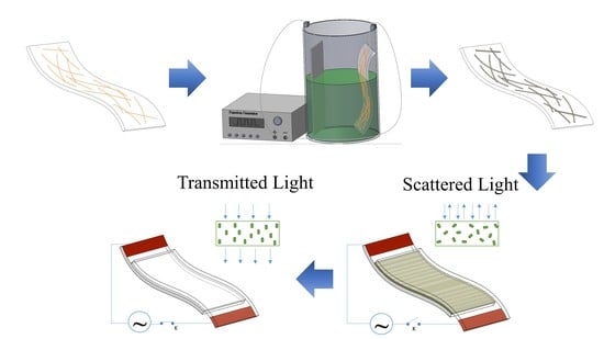
3.4. Flexible Smart Window Fabrication
The mechanical flexibility of Cu–Ni on a PET substrate was investigated by the bending test system with bending radius R = 5 mm and frequency of 0.7 Hz. Two electrodes of Cu NWs and Cu–Ni NWs, which had a sheet resistance of 32, and 27 Ω/sq and a transmittance of 85%, and 76%, respectively, were prepared.
Figure 10a shows them during the bending process from the original state to the bent state then during recovery to the initial state. The electrodes coated on the PET substrate that had a thickness of 50 μm were bent in the middle of the surface. The change of sheet resistance of the two electrodes after the bending test is shown in
Figure 10b. During the test, where R
0 is the initial measured resistance, the change in resistance (∆R = R − R
0) was measured for each sample, and R is the resistance measured under bending. As can be seen in
Figure 10b, both the sheet resistance of the Cu NWs and Cu–Ni NWs electrodes increased slightly when bending in the first 4000 cycles. Subsequently, when the number of cycles increased up to 6000, the sheet resistance of the Cu NW electrodes increased significantly due to delamination, whereas there was only a slight increase in the sheet resistance of the Cu–Ni NW electrodes. As a result, the Cu–Ni NWs exhibit high flexibility, making them quite appropriate for various applications in which flexibility is important.
Figure 11 shows the photographs of flexible PDLC smart windows with 2 Cu–Ni electrodes on PET film prepared by PC plating in the “ON state” and “OFF state”. They had a sheet resistance of 27 Ω/sq and a transmittance of 76% at a wavelength of 550 nm. In fact, the reddish color of Cu NW electrodes makes them unsuitable for optical applications. Therefore, a change to using the gray color of the Cu–Ni NWs electrodes as shown in
Figure 11 was an appropriate solution. The operation of the smart windows is illustrated by the schematic in
Figure 2 and photographs in
Figure 11. When voltage was applied, the opaque state immediately changed to the transparent state. This can be explained because the “OFF state” reduces the passage of light through to the polymer layer due to randomly oriented microdroplets. In the “ON state”, the light can be transmitted through the PDLC smart window because of the alignment of the microdroplets, therefore the text line behind the window is seen more clearly. Moreover, the window operated normally when the voltage was applied in the bending state, hence demonstrating the suitability and potential use of the Cu–Ni NW electrodes in flexible applications.
Figure 12a shows the transmittance of the Cu–Ni NW-based PDLC smart window in the “ON” and “OFF” states as a function of wavelengths from 350 nm to 800 nm. As a result, the difference in transparency at 550 nm between the on- and off-state for the nanowire-based device, ΔT
on–off was 47.5% (69% in the on-state and 21.5% in the off-state). Moreover, as shown in
Figure 12b, the transmittance of the window increased when the applied voltage was increased and reached 90% of its maximum transmittance at 50 V. As a result, the windows exhibited a transmittance of 63% using an applied voltage of 50 V.


