Abstract
The present research front of NbO2 based memory, energy generation, and storage thin film devices is reviewed. Sputtering plasmas contain NbO, NbO2, and NbO3 clusters, affecting nucleation and growth of NbO2, often leading to a formation of nanorods and nanoslices. NbO2 (I41/a) undergoes the Mott topological transition at 1081 K to rutile (P42/mnm), yielding changes in the electronic structure, which is primarily utilized in memristors. The Seebeck coefficient is a key physical parameter governing the performance of thermoelectric devices, but its temperature behavior is still controversial. Nonetheless, they perform efficiently above 900 K. There is a great potential to improve NbO2 batteries since the theoretical capacity has not been reached, which may be addressed by future diffusion studies. Thermal management of functional materials, comprising thermal stress, thermal fatigue, and thermal shock, is often overlooked even though it can lead to failure. NbO2 exhibits relatively low thermal expansion and high elastic modulus. The future for NbO2 thin film devices looks promising, but there are issues that need to be tackled, such as dependence of properties on strain and grain size, multiple interfaces with point and extended defects, and interaction with various natural and artificial environments, enabling multifunctional applications and durable performance.
1. Introduction
NbO2 (space group I41/a (distorted rutile), above 1081 K space group P42/mnm (rutile)) [1] is a binary system belonging to a common class of rutile oxides, comprising SiO2, TiO2, VO2, CrO2, MnO2, GeO2, NbO2, RuO2, RhO2, SnO2, TaO2, OsO2, IrO2, and PbO2 [2,3]. Even though Nb can readily form other binary oxides, such as NbO and Nb2O5 [1], NbO2 is an emerging compound prone to yield many exciting cutting-edge applications. NbO2 exhibits an amalgam of remarkable physical and chemical properties [4], including one of the highest Mott transition temperature (1081 K) [5,6,7], high specific capacity in Li ion batteries (up to 225 mAhg−1) [8,9], large relative dielectric constant (approx. 10) [10,11], large Seebeck coefficient (order of −200 μV K−1) [12,13,14,15], enhanced catalytic activity towards H2 [16] and N2 [17] as well as oxygen reduction reactions [18]. Moreover, further characteristics are known such as superconductivity at 5 K when intercalated with Li [19], a relatively low linear coefficient of thermal expansion (4.8 ppm K−1 at 373 K) [20], and low fluence of 2 mJ cm−2 required for optical excitations [21]. NbO2 is identified to form different types of nanostructures, including nanorods [11] and nanoslices [10,22]. Such attractive properties give rise to many high-tech applications of NbO2 (see Figure 1), including, but not limited to, memristors [23,24,25], x-point memory arrays [26], electro-optic switching [27,28,29], diodes and electron emitters [10,11], fuel cells [18], batteries [8,9], surface catalysis [16,17,18], and thermoelectric devices [14,15].
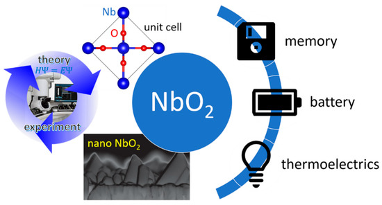
Figure 1.
Synergy of theoretical and experimental methods employed on nanostructured NbO2 to open up possibilities for many high-tech applications. This review is congregated around memory and energy thin film devices.
It is needless to say that microelectronic devices are nowadays thin films and they are also important for the majority of other applications of NbO2 stated above. Of the two major thin film synthesis methods, physical and chemical vapor deposition, NbO2 has been grown using the former, predominantly magnetron sputtering [13,22,27,28,29,30]. However, also pulsed laser deposition [6], electron [31] or ion [32] beam evaporation and molecular beam epitaxy [33] can be employed. In addition, NbO2 also forms by oxidation of Nb [34], alike to oxidation of other metals related to rutile oxides such as Zr [35]. Hence, this review focuses on sputtered thin films because it is the most common synthesis route for NbO2, it is environmentally friendly, it is relatively easy to control and it is frequently used in industry. Furthermore, sputtering offers the possibility to utilize ion-surface interactions to achieve a desired microstructure or texture and enable nanostructuring.
Density functional theory (DFT) [36,37] is a quantum mechanical method frequently used in materials science, physics, chemistry and even in biology to some extent. Through employment of such techniques, the electronic structure of a ground state can be related to physical and chemical properties, enabling predictions of novel materials and previously unknown mechanisms as well as providing insights into already identified experimental phenomena. Synergistic merging of DFT and experiments (see Figure 1) is a very potent approach to understand and advance many fields driven by applications. Hence, this review is focused on synergy aided advances of NbO2 thin films pertaining to cutting-edge applications (see Figure 1), including memory as well as energy generation and storage devices. Transport, thermal and mechanical properties are discussed in this review with respect to the electronic structure and performance. While the importance of the electrical and thermal properties may be self-evident for the said applications of NbO2, the mechanical properties are also of significance as secondary features, being an integral part of thermal stress, thermal fatigue, and thermal shock [38], which cannot be ignored in modern design endeavors of microelectronic, energy generation and storage devices.
2. Nucleation and Growth
Magnetron sputtering is a plasma based physical vapor deposition technique that is commonly employed to synthesize NbO2 thin films [13,22,27,28,29,30]. Both plasma energetics and composition are relevant for surface diffusion processes governing the nucleation and growth of sputtered thin films [39]. Oxygen ions exhibit a broad energy distribution according to the analysis of Nb–O2–Ar sputtering plasma [40]. In addition, increasing Nb oxidation states up to Nb2+ are observed upon increasing energy input into a sputtering target [41]. A considerable amount of plasma composition insights has been gained from high-energy molecular beam experiments revealing that Nb can form a variety of clusters with O in the gas phase, such as NbO, NbO2, NbO3, Nb2O4, Nb2O5, Nb2O6, Nb3O6, Nb3O7, Nb3O8, Nb4O9, Nb4O10, Nb4O11, Nb5O11, Nb5O12 and Nb5O13 [42,43]. Some of these Nb containing clusters have also been detected in sputtering plasmas, namely NbO, NbO2 and NbO3 [44], as depicted in Figure 2. This is not common for sputtering plasmas and should affect the growth processes of NbO2. Nb and clusters containing Nb on NbO2(001) surface exhibit strong adsorption (adsorption energies in the order of −7.2 to −10.1 eV) [44]. These species are not very mobile, but if there is any surface diffusion, it occurs along the <110> direction, characterized by hopping from one lattice site to another [44]. By tuning the plasma composition (O2 partial pressure) to prevent the formation of NbO3 clusters, unwanted NbO clusters are still present when synthesizing NbO2 thin films [44]. This may lead to a growth disruption and recurring nucleation. However, even though high crystalline quality may be challenging to achieve under such conditions, this may be of relevance for nanostructuring, which is discussed below. It is interesting to remark that the NbO2 clusters in an amorphous Nb–O matrix are energetically more stable than the NbO clusters by 44 meV atom−1 [45], giving rise to stable nuclei and formation of NbO2.
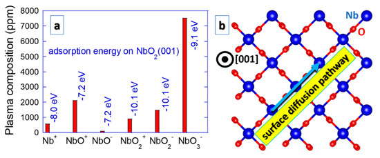
Figure 2.
Composition of Nb–O2–Ar sputtering plasma regarding Nb containing species [44] (a). Adsorption energies on NbO2(001) surfaces (a) are provided together with a predominant diffusion pathway [44] (b).
Once stable NbO2 nuclei form in an amorphous matrix or (epitaxially) on a suitable substrate, thin film growth proceeds and the microstructure evolves. Commonly, thin films grow in a columnar (3D) manner, but a layer-by-layer (2D) growth is also possible [39]. Typically, sputtered NbO2 thin films are not epitaxial (2D), unlike samples obtained by pulsed laser deposition [6] or molecular beam epitaxy [46]. This may be due to unwanted NbO clusters present in the sputtering plasma, as discussed above. The ground state structure of NbO2 is body centered tetragonal (bct) [47], but as seen in Figure 3, the Mott transition at 1081 K [5,6,7] gives rise to a local ordering of bct NbO2. Such transition yields changes in the electronic structure (band gap filling) [48] and hence all physical and chemical properties are altered. It is accompanied by the dimerization of Nb atom pairs along the c axis (in the [001] direction), which are disordered in the pristine bct structure, that restore the local symmetry in the rutile structure. The conventional cell of bct NbO2 with 32 formula units is thus reduced to only 2 in rutile NbO2 [5,6,7]. However, the precise underlying atomic mechanisms are still not clear. Nevertheless, it is worth noting that the Mott transition temperature of NbO2 can be affected by alloying or doping [32,49] and photons [21]. Moreover, strain may influence the transition temperature [50], but it is very often overlooked or even neglected.
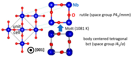
Figure 3.
Mechanism of the Mott transition in NbO2. Symmetry breaking (disordered atomic positions in bct NbO2) is disabled at elevated temperatures where the rutile structure is stabilized.
Memristor is a high-performance non-volatile memory device that stores information in the form of electrical resistance [51]. There are cation and anion type of memristors [51], whereby NbO2 belongs to the latter class. A lower valance state of Nb in NbO2 than in Nb2O5 gives rise to oxygen migration, which is an analogue of an electron motion in a semiconductor. A non-linear behavior of the electrical resistance in NbO2 memristors is enabled by the Mott topological transition [23,24,25] from high resistance bct to low resistance rutile. Hence, a detailed atomistic understanding of the Mott transition in NbO2 is a prerequisite and necessary to advance memristor devices based thereon. Other phase change memory devices include amorphous-crystalline transition materials, such as Ge–Sb–Te alloys [52,53]. Hence, it would be exciting to explore amorphous-crystalline transitions in NbO2 for memory applications, but this has not been exploited so far.
After addressing the nucleation and growth aspects as well as the key structural features driving the Mott transition in NbO2, nanostructuring is addressed. Nanostructures exhibit striking, new physical and chemical properties as well as enable many cutting-edge applications [54,55]. For example, electron mobility is considerably altered in nanostructures [56]. Essentially any application pertaining to large surface areas benefits from nanostructuring, such as memory, energy generation and storage, microelectronics, food packaging and health industry, to name but a few [54,55]. Various nanostructures are known, ranging from nanorods (nanowires), nanorings, nanotubes, nanoslices (nanoplatelets) and nanoribbons, to nanoshells [54,55]. However, nanoslices have been investigated to a considerably less extent than other nano counterparts. They can be perceived as a thick adaptation of graphene [57], which is an exciting 2D model system that offers a tremendous potential for novel applications.
While NbO2 nanorods [11], as in the case of isostructural [58,59] and RuO2 [60,61,62], seem to be common, NbO2 nanoslices [10] are less explored. NbO2 nanoslices were synthesized by thermal oxidation [10], while NbO2 nanorods were formed by hot-filament metal-oxide vapor deposition [11]. Both synthesis techniques are close to thermodynamic equilibrium and the samples were grown under similar conditions, but the structure evolution is drastically different as magnetron sputtering (see Figure 4) gives rise to nanoslices [22]. DFT has been employed to elucidate the underlying growth mechanisms. For the NbO2(110) surfaces, nanoslices are more stable [22], while nanorods are more stable than nanoslices for NbO2(001) [22]. A correlation to Nb–O clusters obtained in sputtering plasmas is still not established, but it may have relevance based on the hypothesis that large clusters act as nucleation sites for RuO2 nanorods [60,61,62]. Furthermore, Nb2O5 forms nanobelts [63] and nanotubes [64], but it is not known if such nanostructures are feasible for NbO2.
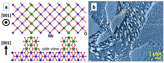
Figure 4.
NbO2 nanoslices: (a) A theoretical model; (b) a secondary electron microscopy image of a corresponding sample (a micrograph of an equivalent sample published in the literature [22]).
3. Electrical Properties
Besides memory applications, NbO2 exhibits a huge potential for renewable energy generation and storage, enabling carbon neutral technologies. The notion of a net zero carbon footprint in conjunction with cheap energy sources is supported with thermoelectrics. Thermoelectric devices directly convert heat into electricity without CO2 emission [65,66]. However, due to the relatively low efficiency of such devices, applications are limited to off-grid uses (e.g., unmanned remote facilities and cathodic protection of pipelines), powering space probes and satellites, waste heat recovery, as well as cooling [65,66]. Strategies to enhance the efficiency (ZT = S2 σ T/κ) at a temperature T involve maximizing the Seebeck coefficient (S) and electrical conductivity (σ), while minimizing the thermal conductivity (κ) [65,66].
The behavior of the Seebeck coefficient of NbO2 is still controversial. Figure 5 shows the Seebeck coefficient and power factor (S2 σ) data for NbO2 compared with other oxide systems. Crystalline and amorphous NbO2 exhibit an increasing trend in the absolute value of the Seebeck coefficient as a function of temperature reaching approx. −200 μV K−1 at 900 K according to Music et al. [13] and Backhaus-Ricoult et al. [14]. The amorphous samples outperform the crystalline ones, which is consistent with the generic notion put forward by Nolas et al. [67]. According to DFT results, this behavior is related to band gap filling [13], which is a common physical origin of the Seebeck coefficient enhancement [68]. However, these Seebeck coefficient data (trends) are inconsistent with the work of Roberson et al. [15]. This conundrum remains unresolved (see Figure 5). Nevertheless, all the Seebeck coefficient data converge at about 900 K, indicating that NbO2 thermoelectric devices certainly perform well at high temperatures.
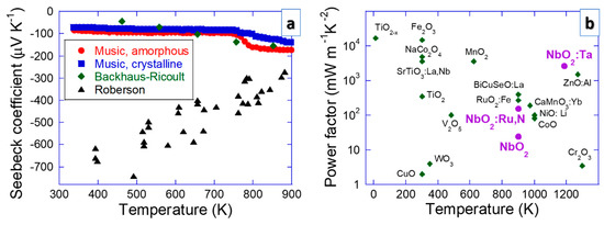
Figure 5.
The electrical properties, including (a) the Seebeck coefficient (Music et al. [13], Backhaus-Ricoult et al. [14], Roberson et al. [15]) and (b) power factor data, for NbO2 compared with other oxide systems [67,68,69,70,71,72,73,74,75,76,77,78,79,80,81,82,83,84]. The power factor is a product of the squared Seebeck coefficient and electrical conductivity.
Using DFT, more than 20 elements were studied to find candidates that could outdo the absolute value of the Seebeck coefficient of amorphous NbO2 [85,86]. Comparing the measured power factor (S2σ) of NbO2 with other oxides, including isostructural TiO2−x [69], TiO2 [70], MnO2 [71] and RuO2:Fe [72], as well as Fe2O3 [73], NaCo2O4 [74], SrTiO3:La,Nb [75], V2O5 [76], WO3 [77], CuO [78], BiCuSeO:La [79], ZnO:Al [80], CaMnO3:Yb [81], NiO:Li [82], CoO [83] and Cr2O3 [84] (see Figure 5), it is evident that NbO2:Ta performs better than ZnO:Al [80], which is the major oxide competitor in the high temperature range. This is exciting since Nb is less toxic than Zn, proving a good alternative.
It is clear that the electrical conductivity (up to 30 kS m−1 at 1100 K [14]) is high enough to enable efficient thermoelectric NbO2 devices (see Figure 5) and the Frenkel-Poole conduction (anion vacancy mediated) mechanism appears to be of relevance [87]. Other phenomena pertaining to conductivity have been less treated. For instance, ionic conductivity can readily be detrimental in several applications. Oxygen diffusion is relevant for memristors, hydrogen for fuel cells and Li for use in Li ion batteries. In the case of thermoelectric devices, which are frequently exposed to elevated temperatures, diffusion can also be relevant since there are many interfaces in commercial systems (e.g., metallic contacts). Even though the Mott transition is a diffusion-less process (see Figure 3), interfaces to other layers may affect it (e.g., intermixing with Ti from a TiN layer was reported to lower the Mott transition temperature in NbO2 [30]). Most of the research along these lines was carried out for Li ion batteries. The activation energy for Li diffusion in NbO2 with W additions (NbO2:W) is 0.1–0.3 eV [88], allowing for a specific capacity up to 225 mAhg−1 in pristine NbO2 [8,9] as well as in NbO2:W [88]. The theoretical capacity of 429 mAhg−1 in NbO2 has not yet been reached [9]. It might be enhanced by increasing the electrical conductivity [89], an effort also conducive to thermoelectric devices. It also seems that NbO2 show potential for redox flow batteries [90]. Further studies of alloying/doping and nanostructuring may be beneficial for batteries.
4. Thermal Properties
A property remaining to be tackled to fully describe thermoelectric devices is thermal conductivity. The thermal conductivity data have been obtained just recently. NbO2(001) and NbO2(110) surfaces exhibit the value of 3.0 and 2.9 W m−1 K−1 [91], respectively (see Figure 6). Upon nanostructuring of amorphous NbO2 by multilayering with Ta-Ni-O, it can further be reduced to 0.6 W m−1 K−1 [45], which is desired for thermoelectric devices to increase the efficiency (ZT).
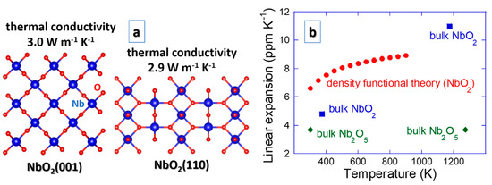
Figure 6.
Thermal properties of NbO2, including (a) thermal conductivity for two orientations [91] and (b) linear coefficient of thermal expansion obtained theoretically [92] and experimentally [20]. Due to a lack of other values, a comparison is made with the available expansion data on Nb2O5 [93].
Thermal management of functional materials, including thermal stress, thermal fatigue and thermal shock [38], is often overlooked or ignored even though it can easily lead to fracture and ultimately failure. For instance, thermoelectric devices do not comprise any movable parts, but cyclic thermal loading can give rise to thermal fatigue, a secondary physical property. Thermal expansion is an integral part of thermal stress, thermal fatigue and thermal shock [38], but such data are not often available, especially not for thin films. Figure 6 contains the linear coefficient of thermal expansion data for NbO2 obtained theoretically [92] and experimentally [20]. Due to a lack of other literature values, a comparison is made with the available thermal expansion data on Nb2O5 [93], pointing out that the general trends for NbO2 are sound. However, some improvements for the NbO2 data may be possible as theoretical and measured slopes are not entirely within the expected margins. An overlooked incentive for scattering of the thermal expansion data may be its grain size dependence [94].
Other thermal properties, such as heat capacity, are less explored. In the evaluation of binary Nb–O phase diagrams, it is accepted that the isobaric molar heat capacity of NbO2 is in the order of 55 J mol−1 K−1 at room temperature [47], which is relatively high for solids. However, it is not known if and how the heat capacity is affected by nanostructuring or other factors (e.g., strain). Clearly, much more work on the thermal properties of NbO2 is needed.
5. Mechanical Properties
Mechanical properties are certainly secondary properties for memory and energy related applications of NbO2, but equivalent to the thermal expansion data discussed above they are central for thermal stress, thermal fatigue and thermal shock [38]. Hence, such aspects cannot be ignored in more realistic design endeavors of novel devices. First, elastic properties are addressed, as compiled in Figure 7. Owing to the tetragonal symmetry (P42/mnm), the rutile structure exhibits seven independent elastic constants, which along with their temperature and pressure dependence have been investigated by means of ultrasonic wave velocity measurements [95,96,97,98]. The reported data are generally consistent between the different references and at room temperature the elastic constants are C11 = 433 GPa, C12 = 93 GPa, C13 = 173 GPa, C33 = 388 GPa, C44 = 94 GPa and C66 = 57 GPa, whereas C16 for all practical purposes can be considered negligible [95]. The DFT [92] and bulk (the Voigt–Reuss–Hill average) [95] data for the elastic (Young’s) modulus of NbO2 differ only by 4%. The available thin film values are not straightforward to compare with. The crystalline thin film is porous [99] and the amorphous sample contains Ta [85]. Moreover, the penetration depth during the nanoindentation experiments was 15–20% for pure NbO2 thin films [99] and 10% for NbO2 with Ta additions [85]. This measuring inconsistency is of relevance for the comparison of mechanical properties, but as of yet there are no systematic studies to gain more insights. Nevertheless, it seems that the elastic modulus of NbO2 is quite high, being 64% of the value of sapphire which is a well-known stiff and hard material [100]. Such a high value can be rationalized by strongly hybridized Nb 5d–O 2p states [5]. In the light of these findings, it seems that reduced thermal stresses (product of thermal expansion, elastic modulus and boundary conditions), which can be achieved by minimization of elastic modulus, are feasible through the employment of amorphous and/or porous (or nanostructured) NbO2.
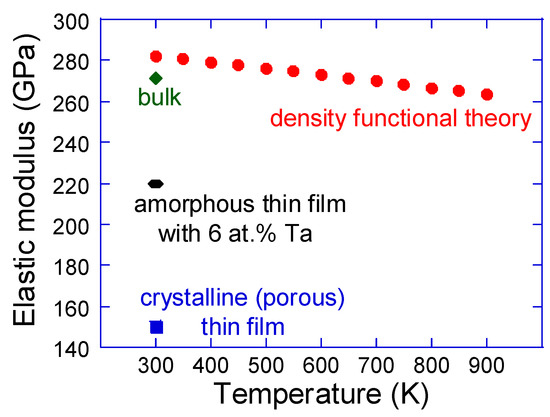
Figure 7.
Elastic (Young’s) modulus as a function of temperature. Density functional theory data for ideal NbO2 [92] are compared with the bulk value [95] as well as crystalline [99] and amorphous [85] thin films. It should be noted that the crystalline thin film is porous [99] and the amorphous sample contains Ta [85], making the comparison less straightforward.
Characterization of further mechanical properties of NbO2 is a rather uncharted territory compared to other more commonly considered rutile oxides, e.g., TiO2. Using the elasticity data presented above, the Debye temperature can be derived to be 597 K at low temperature, reaching ~590 K at room temperature [96,97]. Furthermore, the Cauchy pressure [101] is positive with C13–C44 = 79 GPa and C12 −C66 = 36 GPa, indicating that a ductile response of NbO2 may be expected, but little is known about its yield properties. Except for some measurements on sputtered films [99], there is a lack of experimental data regarding hardness for NbO2, which is critical for, e.g., wear resistance. This emphasizes the need to explore such properties. For thin and porous films, the nanohardness values have been measured to correspond to 6 GPa [99], which most likely is an underestimation of that for compact NbO2. Based on the Voigt–Reuss–Hill averages of the elastic constants in conjunction with the empirical relation between the bulk and shear moduli and Vickers hardness by Chen et al. [102], it can be estimated to be 8 GPa. Although this theoretical estimate is uncertain, it is comparable to that of rutile TiO2 [103], which has been classified as 6–6.5 on the Mohs hardness scale.
The impact that dislocations can have on physical properties, such as transport properties, of rutile transition metal oxides is well-documented [104]. However, the available literature on NbO2 is scarce and would from both mechanical and physical perspectives benefit from further investigations. In terms of plasticity of other rutile structures, edge dislocations have been known to exist on {100}, {101} and {110} planes [105,106,107,108]. Experiments have shown that the slip activated systems to accommodate plastic deformation correspond to the and type slip systems [105,106]. Based on results from nanoindentation experiments of TiO2 single crystals, a directional dependence of the activated slip planes has been observed, where indentation onto (001) surfaces yields activation of all four slip systems, while for the (100) surface only two of the slip systems in tandem with are activated [108]. Due to intersection of slip planes for the former, the dislocation motion is generally inhibited, which indicates an increased hardening for (001) surfaces [108]. Hence, many mechanical properties are still unexplored for NbO2, including the physical origin thereof.
6. Summary and Outlook
NbO2 is an emerging binary oxide with many exciting cutting-edge applications, such as memory as well as energy generation and storage devices, owing to an amalgam of its physical and chemical properties. In the present work, transport, thermal and mechanical properties are reviewed with respect to the electronic structure. Sputtering plasmas contain NbO, NbO2 and NbO3 clusters, influencing nucleation and growth of NbO2. They adsorb strongly, whereby unwanted NbO clusters likely lead to a growth disruption and recurring nucleation, which may be of relevance for nanostructuring (formation of nanorods and nanoslices). Low temperature bct NbO2 undergoes the Mott transition at 1081 K, where pairs of Nb atoms dimerize along the c axis, stabilizing rutile NbO2. The Mott transition yields changes in the electronic structure (band gap filling), alerting all physical and chemical properties. These structural changes are primarily used in memristors. Beside memory applications, NbO2 exhibits a huge potential for renewable energy generation and storage, enabling carbon neutral technologies. One example is found within thermoelectric devices, chiefly governed by the Seebeck coefficient. However, there are reports with opposing trends thereof as a function of temperature. Nevertheless, all the Seebeck coefficient data converge to about −200 μV K−1 at 900 K so that at least at this high temperature NbO2 thermoelectric devices certainly perform well. Electrical conductivity is high enough to enable efficient thermoelectric NbO2 devices, but research on its ionic conductivity, including oxygen for memristors, hydrogen for fuel cells and Li for use in Li ion batteries, seems to be at its infancy. Most of the research along these lines has been carried out for Li ion batteries, but their theoretical capacity has not yet been reached. Thermal management of functional materials, including thermal stress, thermal fatigue and thermal shock, is often overlooked or ignored even though it can easily promote fracture and subsequent failure. NbO2 exhibits relatively low thermal expansion, but high elastic modulus, which can be attributed to strong Nb–O hybridization. To minimize the thermal stress, elastic modulus should be reduced, which seems to be possible in amorphous and nanostructured NbO2. Plasticity of NbO2 is yet to be explored.
The future of NbO2 thin film devices is indeed very promising, but there are many issues that should be tackled both by DFT and experimentation. Many applications should further be addressed, including, e.g., fuel cells. It is often ignored that most of the physical and chemical properties are dependent on the loading conditions and microstructure, e.g., strain and grain size. These factors generally affect the electronic structure and all physical and chemical properties, but studies to gain insights into such behavior are still at infancy for NbO2. Such aspects need to be evaluated to bring insight to their impact and severity. Nanostructuring should be further explored to enable decoupling of electrical and thermal conductivity in thermoelectric devices (enhancement of ZT) and larger surface areas in batteries (short diffusion pathways for Li ions enabling higher charge/discharge rates). Although NbO2 forms nanorods and nanoslices, it remains to be seen if other nanostructures, such as nanobelts and nanotubes, can be formed to trigger further applications. Commercial devices often include many layers besides the key functional materials (e.g., metallic contacts), which is often overlooked in fundamental studies. This means that multiple interfaces must be explored and the interplay with point and extended defects, such as dislocations. Finally, interaction with non-ideal environments (e.g., atmosphere, biological tissue, etc.) should be explored for the purpose of enabling novel multifunctional applications.
Author Contributions
D.M. conceived the manuscript. All authors contributed to the evaluation and interpretation of the published data in previous works. The manuscript was primarily written by D.M. with extended inputs from A.M.K. and P.A.T.O. All authors have read and agreed to the published version of the manuscript.
Funding
This research received no external funding.
Institutional Review Board Statement
Not applicable.
Informed Consent Statement
Not applicable.
Data Availability Statement
Data sharing is not applicable to this article.
Conflicts of Interest
The authors declare no conflict of interest.
References
- Nico, C.; Soares, M.R.N.; Rodrigues, J.; Matos, M.; Monteiro, R.; Graça, M.P.F.; Valente, M.A.; Costa, F.M.; Monteiro, T. Sintered NbO powders for electronic device applications. J. Phys. Chem. C 2011, 115, 4879. [Google Scholar] [CrossRef]
- Baur, W.H. Rutile-type compounds. Acta Cryst. B 1976, 32, 2200. [Google Scholar] [CrossRef]
- Maddox, B.R.; Yoo, C.S.; Kasinathan, D.; Pickett, W.E.; Scalettar, R.T. High-pressure structure of half-metallic CrO2. Phys. Rev. B 2006, 73, 144111. [Google Scholar] [CrossRef]
- Lorenz, M.; Rao, M.S.R.; Venkatesan, T.; Fortunato, E.; Barquinha, P.; Branquinho, R.; Salgueiro, D.; Martins, R.; Carlos, E.; Liu, A.; et al. The 2016 oxide electronic materials and oxide interfaces roadmap. J. Phys. D Appl. Phys. 2016, 49, 433001. [Google Scholar] [CrossRef]
- O’Hara, A.; Nunley, T.N.; Posadas, A.B.; Zollner, S.; Demkov, A.A. Electronic and optical properties of NbO2. J. Appl. Phys. 2014, 116, 213705. [Google Scholar] [CrossRef]
- Joshi, T.; Senty, T.R.; Borisov, P.; Bristow, A.D.; Lederman, D. Preparation, characterization, and electrical properties of epitaxial NbO2 thin film lateral devices. J. Phys. D Appl. Phys. 2015, 48, 335308. [Google Scholar] [CrossRef]
- Bolzan, A.A.; Fong, C.; Kennedy, B.J.; Howard, C.J. A powder neutron diffraction study of semiconducting and metallic niobium dioxide. J. Solid State Chem. 1994, 113, 9. [Google Scholar] [CrossRef]
- Ji, Q.; Gao, X.; Zhang, Q.; Jin, L.; Wang, D.; Xia, Y.; Yin, S.; Xia, S.; Hohn, N.; Zuo, X.; et al. Dental resin monomer enables unique NbO2/carbon lithium-ion battery negative electrode with exceptional performance. Adv. Funct. Mater. 2019, 29, 1904961. [Google Scholar] [CrossRef]
- Kim, Y.-S.; Cho, Y.; Nogales, P.M.; Jeong, S.-K. NbO2 as a noble zero-strain material for Li-Ion batteries: Electrochemical redox behavior in a nonaqueous solution. Energies 2019, 12, 2960. [Google Scholar] [CrossRef]
- Zhao, Y.; Zhang, Z.; Lin, Y. Optical and dielectric properties of a nanostructured NbO2 thin film prepared by thermal oxidation. J. Phys. D Appl. Phys. 2004, 37, 3392. [Google Scholar] [CrossRef]
- Lin, J.-H.; Patil, R.A.; Wu, M.-A.; Yu, L.-G.; Liu, K.-D.; Devan, W.-T.G.R.S.; Ho, C.-H.; Liou, Y.; Ma, Y.-R. Large-area nanoscale farmland-like surfaces of one-dimensional NbO2 nanorods with multigrowth directions: Studies on the purple-blue photoluminescence and low-field electron emissions. J. Mater. Chem. C 2014, 2, 8667. [Google Scholar] [CrossRef]
- Rahman, J.U.; Meang, E.-J.; Nguyen, D.V.; Seo, W.-S.; Hussain, A.; Kim, M.H.; Lee, S. The synthesis and thermoelectric properties of p-type Li1-xNbO2-based compounds. J. Electron. Mater. 2017, 46, 1740. [Google Scholar] [CrossRef]
- Music, D.; Chen, Y.-T.; Bliem, P.; Geyer, R.W. Amorphous-crystalline transition in thermoelectric NbO2. J. Phys. D Appl. Phys. 2015, 48, 275301. [Google Scholar] [CrossRef]
- Backhaus-Ricoult, M.; Rustad, J.; Moore, L.; Smith, C.; Brown, J. Semiconducting large bandgap oxides as potential thermoelectric materials for high-temperature power generation? Appl. Phys. A 2014, 116, 433. [Google Scholar] [CrossRef]
- Roberson, J.A.; Rapp, R.A. Electrical properties of NbO and NbO2. J. Phys. Chem. Solids 1969, 30, 1119. [Google Scholar] [CrossRef]
- Isobe, S.; Kudoh, K.; Hino, S.; Hara, K.; Hashimoto, N.; Ohnuki, S. Catalytic efficiency of Nb and Nb oxides for hydrogen dissociation. Appl. Phys. Lett. 2015, 107, 081602. [Google Scholar] [CrossRef]
- Huang, L.; Wu, J.; Han, P.; Al-Enizi, A.M.; Almutairi, T.M.; Zhang, L.; Zheng, G. NbO2 electrocatalyst toward 32% faradaic efficiency for N2 fixation. Small Methods 2019, 3, 1800386. [Google Scholar] [CrossRef]
- Sun, J.; Sun, W.; Du, L.; Du, C.; Gao, Y.; Yin, G. Tailored NbO2 modified Pt/graphene as highly stable electrocatalyst towards oxygen reduction reaction. Fuel Cells 2018, 18, 360. [Google Scholar] [CrossRef]
- Geselbracht, M.J.; Richardson, T.J.; Stacy, A.M. Superconductivity in the layered compound LixNbO2. Nature 1990, 345, 324. [Google Scholar] [CrossRef]
- Sakata, K. Note on the phase transition in NbO2. J. Phys. Soc. Jpn. 1969, 26, 582. [Google Scholar] [CrossRef]
- Beebe, M.R.; Klopf, J.M.; Wang, Y.; Kittiwatanakul, S.; Lu, J.; Wolf, S.A.; Lukaszew, R.A. Time-resolved light-induced insulator-metal transition in niobium dioxide and vanadium dioxide thin films. Opt. Mater. Express 2017, 7, 213. [Google Scholar] [CrossRef]
- Music, D.; Geyer, R.W. Theoretical and experimental study of NbO2 nanoslice formation. J. Phys. D Appl. Phys. 2015, 48, 305302. [Google Scholar] [CrossRef]
- Kumar, S.; Strachan, J.P.; Williams, R.S. Chaotic dynamics in nanoscale NbO2 Mott memristors for analogue computing. Nature 2017, 548, 318. [Google Scholar] [CrossRef]
- Leon, J.J.D.; Norris, K.J.; Yang, J.J.; Sevic, J.F.; Kobayashi, N.P. A niobium oxide-tantalum oxide selector-memristor self-aligned nanostack. Appl. Phys. Lett. 2017, 110, 103102. [Google Scholar] [CrossRef]
- Lee, J.; Kim, J.; Kim, T.; Sohn, H. Effect of Pt top electrode deposition on the valence state and resistance switching behavior of NbO2-x. J. Mater. Sci. Mater. Electron 2020, 31, 14384. [Google Scholar] [CrossRef]
- Park, J.; Hadamek, T.; Posadas, A.B.; Cha, E.; Demkov, A.A.; Hwang, H. Multi-layered NiOy/NbOx/NiOy fast drift-free threshold switch with high Ion/Ioff ratio for selector application. Sci. Rep. 2017, 7, 4068. [Google Scholar] [CrossRef]
- Lee, J.C.; Durand, W.W. Electrically stimulated optical switching of NbO2 thin films. J. Appl. Phys. 1984, 56, 3350. [Google Scholar] [CrossRef]
- Wong, F.J.; Hong, N.; Ramanathan, S. Orbital splitting and optical conductivity of the insulating state of NbO2. Phys. Rev. B 2014, 90, 115135. [Google Scholar] [CrossRef]
- Lee, J.H.; Cha, E.J.; Kim, Y.T.; Chae, B.K.; Kim, J.J.; Lee, S.Y.; Hwang, H.S.; Park, C.G. A study of threshold switching of NbO2 using atom probe tomography and transmission electron microscopy. Micron 2015, 79, 101. [Google Scholar] [CrossRef]
- Zhang, J.; Norris, K.J.; Gibson, G.; Zhao, D.; Samuels, K.; Zhang, M.M.; Yang, J.J.; Park, J.; Sinclair, R.; Jeon, Y.; et al. Thermally induced crystallization in NbO2 thin films. Sci. Rep. 2016, 6, 34294. [Google Scholar] [CrossRef]
- Wang, P.; Khan, A.I.; Yua, S. Cryogenic behavior of NbO2 based threshold switching devices as oscillation neurons. Appl. Phys. Lett. 2020, 116, 162108. [Google Scholar] [CrossRef]
- Wang, Y.; Zhang, J.; Ni, Y.; Chen, X.; Mescall, R.; Isaacs-Smith, T.; Comes, R.B.; Kittiwatanakul, S.; Wolf, S.A.; Lu, J.; et al. Structural, transport, and ultrafast dynamic properties of V1-xNbxO2 thin films. Phys. Rev. B 2019, 99, 245129. [Google Scholar] [CrossRef]
- Noskin, L.E.; Seidner, A.; Schlom, D.G. Growth of NbO2 by molecular-beam epitaxy and characterization of its metal-insulator transition. MRS Adv. 2017, 2, 3031. [Google Scholar] [CrossRef][Green Version]
- Nivedita, L.R.; Haubert, A.; Battu, A.K.; Ramana, C.V. Correlation between crystal structure, surface/interface microstructure, and electrical properties of nanocrystalline niobium thin films. Nanomaterials 2020, 10, 1287. [Google Scholar] [CrossRef]
- Kautz, E.J.; Gwalani, B.; Lambeets, S.V.M.; Kovarik, L.; Schreiber, D.K.; Perea, D.E.; Senor, D.; Liu, Y.-S.; Battu, A.K.; Tseng, K.-P.; et al. Rapid assessment of structural and compositional changes during early stages of zirconium alloy oxidation. NPJ Mater. Degrad. 2020, 4, 29. [Google Scholar] [CrossRef]
- Hohenberg, P.; Kohn, W. Inhomogeneous electron gas. Phys. Rev. 1964, 136, B864–B871. [Google Scholar] [CrossRef]
- Kohn, W.; Sham, L.J. Self-consistent equations including exchange and correlation effects. Phys. Rev. 1965, 140, A1133. [Google Scholar] [CrossRef]
- Case, E.D. Thermal fatigue and waste heat recovery via thermoelectrics. J. Electron. Mater. 2012, 41, 1811. [Google Scholar] [CrossRef]
- Petrov, I.; Barna, P.B.; Hultman, L.; Greene, J.E. Microstructural evolution during film growth. J. Vac. Sci. Technol. A 2003, 21, S117. [Google Scholar] [CrossRef]
- Mráz, S.; Schneider, J.M. Influence of the negative oxygen ions on the structure evolution of transition metal oxide thin films. J. Appl. Phys. 2006, 100, 023503. [Google Scholar] [CrossRef]
- Hála, M.; Čapek, J.; Zabeida, O.; Klemberg-Sapieha, J.E.; Martinu, L. Hysteresis-free deposition of niobium oxide films by HiPIMS using different pulse management strategies. J. Phys. D Appl. Phys. 2012, 45, 055204. [Google Scholar] [CrossRef]
- Deng, H.T.; Kerns, K.P.; Castleman, A.W. Formation, structures, and reactivities of niobium oxide cluster ions. J. Phys. Chem. 1996, 100, 13386. [Google Scholar] [CrossRef]
- Fielicke, A.; Meijer, G.; von Helden, G. Infrared spectroscopy of niobium oxide cluster cations in a molecular beam: Identifying the cluster structures. J. Am. Chem. Soc. 2003, 125, 3659. [Google Scholar] [CrossRef] [PubMed]
- Music, D.; Schmidt, P.; Mráz, S. Adsorption of film-forming species on NbO and NbO2 surfaces. J. Vac. Sci. Technol. A 2017, 35, 061512. [Google Scholar] [CrossRef]
- Music, D.; Prünte, S.; Keuter, P.; Saksena, A. On thermal conductivity of amorphous niobium monoxide. J. Phys. D Appl. Phys. 2020, 53, 285303. [Google Scholar] [CrossRef]
- Posadas, A.; Kvit, A.; Demkov, A.A. Growth of NbO2 thin films on GaN (0001) by molecular beam epitaxy. Thin Solid Film. 2019, 691, 137603. [Google Scholar] [CrossRef]
- Jacob, K.T.; Shekhar, C.; Vinay, M. Thermodynamic properties of niobium oxides. J. Chem. Eng. Data 2010, 55, 4854. [Google Scholar] [CrossRef]
- Liu, Y.; Zhang, H.; Cheng, X. Sequential insulating-metal-insulating phase transition of NbO2 by doping photoexcited carrier. Comput. Mater. Sci. 2020, 173, 109434. [Google Scholar] [CrossRef]
- Kang, M.; Yu, S.; Son, J. Voltage-induced insulator-to-metal transition of hydrogen-treated NbO2 thin films. J. Phys. D Appl. Phys. 2015, 48, 095301. [Google Scholar] [CrossRef]
- Joshi, T.; Cirino, E.; Morley, S.A.; Lederman, D. Thermally induced metal-to-insulator transition in NbO2 thin films: Modulation of the transition temperature by epitaxial strain. Phys. Rev. Mater. 2019, 3, 124602. [Google Scholar] [CrossRef]
- Sun, W.; Gao, B.; Chi, M.; Xia, Q.; Yang, J.J.; Qian, H.; Wu, H. Understanding memristive switching via in situ characterization and device modeling. Nat. Commun. 2019, 10, 3453. [Google Scholar] [CrossRef] [PubMed]
- Sun, Z.; Kyrsta, S.; Music, D.; Ahuja, R.; Schneider, J.M. Structure of the Ge-Sb-Te phase-change materials studied by theory and experiment. Solid State Commun. 2007, 143, 240. [Google Scholar] [CrossRef]
- Wuttig, M.; Yamada, N. Phase-change materials for rewriteable data storage. Nat. Mater. 2007, 6, 824. [Google Scholar] [CrossRef] [PubMed]
- Barth, J.V.; Costantini, G.; Kern, K. Engineering atomic and molecular nanostructures at surfaces. Nature 2005, 437, 671. [Google Scholar] [CrossRef]
- Xia, Y.; Yang, P.; Sun, Y.; Wu, Y.; Mayers, B.; Gates, B.; Yin, Y.; Kim, F.; Yan, H. One-dimensional nanostructures: Synthesis, characterization, and applications. Adv. Mater. 2003, 15, 353. [Google Scholar] [CrossRef]
- Arakawa, Y.; Sakaki, H. Multidimensional quantum well laser and temperature dependence of its threshold current. Appl. Phys. Lett. 1982, 40, 939. [Google Scholar] [CrossRef]
- Novoselov, K.S.; Geim, A.K.; Morozov, S.V.; Jiang, D.; Zhang, Y.; Dubonos, S.V.; Grigorieva, I.V.; Firsov, A.A. Electric field effect in atomically thin carbon films. Science 2004, 306, 666. [Google Scholar] [CrossRef]
- Liu, B.; Aydil, E.S. Growth of oriented single-crystalline rutile TiO2 nanorods on transparent conducting substrates for dye-sensitized solar cells. J. Am. Chem. Soc. 2009, 131, 3985. [Google Scholar] [CrossRef]
- Wang, M.; Huang, C.; Cao, Y.; Yu, Q.; Deng, Z.; Liu, Y.; Huang, Z.; Huang, J.; Huang, Q.; Guo, W.; et al. Dye-sensitized solar cells based on nanoparticle-decorated ZnO/TiO2 core/shell nanorod arrays. J. Phys. D Appl. Phys. 2009, 42, 155104. [Google Scholar] [CrossRef]
- Music, D.; Basse, F.H.-U.; Haβdorf, R.; Schneider, J.M. Synthesis and thermoelectric properties of RuO2 nanorods. J. Appl. Phys. 2010, 108, 013707. [Google Scholar] [CrossRef]
- Lin, Y.-T.; Chen, C.-Y.; Hsiung, C.-P.; Cheng, K.-W.; Gan, J.-Y. Growth of RuO2 nanorods in reactive sputtering. Appl. Phys. Lett. 2006, 89, 063123. [Google Scholar] [CrossRef]
- Music, D.; Breunung, J.; Mráz, S.; Schneider, J.M. Role of RuO3 for the formation of RuO2 nanorods. Appl. Phys. Lett. 2012, 100, 033108. [Google Scholar] [CrossRef]
- Wei, M.; Qi, Z.; Ichihara, M.; Zhou, H. Synthesis of single-crystal niobium pentoxide nanobelts. Acta Mater. 2008, 56, 2488. [Google Scholar] [CrossRef]
- Kobayashi, Y.; Hata, H.; Salama, M.; Mallouk, T.E. Scrolled sheet precursor route to niobium and tantalum oxide nanotubes. Nano Lett. 2007, 7, 2142. [Google Scholar] [CrossRef]
- He, J.; Tritt, T.M. Advances in thermoelectric materials research: Looking back and moving forward. Science 2017, 357, eaak9997. [Google Scholar] [CrossRef] [PubMed]
- Snyder, G.J.; Toberer, E.S. Complex thermoelectric materials. Nat. Mater. 2008, 7, 105–114. [Google Scholar] [CrossRef] [PubMed]
- Nolas, G.S.; Goldsmid, H.J. The figure of merit in amorphous thermoelectrics. Phys. Status Solidi A 2002, 194, 271. [Google Scholar] [CrossRef]
- Liu, Y.; Lan, J.; Xu, W.; Liu, Y.; Pei, Y.-L.; Cheng, B.; Liu, D.-B.; Lin, Y.-H.; Zhao, L.-D. Enhanced thermoelectric performance of a BiCuSeO system via band gap tuning. Chem. Commun. 2013, 49, 8075. [Google Scholar] [CrossRef]
- Tang, J.; Wang, W.; Zhao, G.-L.; Li, Q. Colossal positive Seebeck coefficient and low thermal conductivity in reduced TiO2. J. Phys. Condens. Matter 2009, 21, 205703. [Google Scholar] [CrossRef] [PubMed]
- He, Q.; Hao, Q.; Chen, G.; Poudel, B.; Wang, X.; Wang, D.; Ren, Z. Thermoelectric property studies on bulk TiOx with x from 1 to 2. Appl. Phys. Lett. 2007, 91, 052505. [Google Scholar] [CrossRef]
- Walia, S.; Balendhran, S.; Yi, P.; Yao, D.; Zhuiykov, S.; Weber, M.P.R.; Strano, M.S.; Bhaskaran, M.; Sriram, S.; Kalantar-zadeh, K. MnO2-based thermopower wave sources with exceptionally large output voltages. J. Phys. Chem. C 2013, 117, 9137. [Google Scholar] [CrossRef]
- Music, D.; Chen, Y.-T.; Geyer, R.W.; Bliem, P.; Schneider, J.M. Modulation of transport properties of RuO2 with 3d transition metals. Mater. Res. Express 2014, 1, 045034. [Google Scholar] [CrossRef]
- Rajendran, S.; Rao, V.S. An anomalous behaviour in the phase stability of the system Fe203 and NiO. J. Mater. Sci. 1994, 29, 5673. [Google Scholar] [CrossRef]
- Terasaki, I.; Sasago, Y.; Uchinokura, K. Large thermoelectric power in NaCo2O4 single crystals. Phys. Rev. B 1997, 56, R12685. [Google Scholar] [CrossRef]
- Ravichandran, J.; Siemons, W.; Scullin, M.L.; Mukerjee, S.; Huijben, M.; Moore, J.E.; Majumdar, A.; Ramesh, R. Tuning the electronic effective mass in double-doped SrTiO3. Phys. Rev. B 2011, 83, 035101. [Google Scholar] [CrossRef]
- Bahgat, A.A.; Ibrahim, F.A.; El-Desoky, M.M. Electrical and optical properties of highly oriented nanocrystalline vanadium pentoxide. Thin Solid Film. 2005, 489, 68. [Google Scholar] [CrossRef]
- Hutchins, M.G.; Abu-Alkhair, O.; El-Nahass, M.M.; Abdel-Hady, K. Electrical conduction mechanisms in thermally evaporated tungsten trioxide (WO3) thin films. J. Phys. Condens. Matter 2006, 18, 9987. [Google Scholar] [CrossRef][Green Version]
- Hartung, D.; Gather, F.; Hering, P.; Kandzia, C.; Reppin, D.; Polity, A.; Meyer, B.K.; Klar, P.J. Assessing the thermoelectric properties of CuxO (x = 1 to 2) thin films as a function of composition. Appl. Phys. Lett. 2015, 106, 253901. [Google Scholar] [CrossRef]
- Liu, Y.; Ding, J.; Xu, B.; Lan, J.; Zheng, Y.; Zhan, B.; Zhang, B.; Lin, Y.; Nan, C. Enhanced thermoelectric performance of La-doped BiCuSeO by tuning band structure. Appl. Phys. Lett. 2015, 106, 233903. [Google Scholar] [CrossRef]
- Jood, P.; Mehta, R.J.; Zhang, Y.; Peleckis, G.; Wang, X.; Siegel, R.W.; Borca-Tasciuc, T.; Dou, S.X.; Ramanath, G. Al-doped zinc oxide nanocomposites with enhanced thermoelectric properties. Nano Lett. 2011, 11, 4337. [Google Scholar] [CrossRef] [PubMed]
- Flahaut, D.; Mihara, T.; Funahashi, R.; Nabeshima, N.; Lee, K.; Ohta, H.; Koumoto, K. Thermoelectrical properties of A-site substituted Ca1−xRexMnO3 system. J. Appl. Phys. 2006, 100, 084911. [Google Scholar] [CrossRef]
- Shin, W.; Murayama, N. Li-doped nickel oxide as a thermoelectric material. Jpn. J. Appl. Phys. 1999, 38, L1336. [Google Scholar] [CrossRef]
- Kowalski, K.; Ijjaali, M.; Bak, T.; Dupre, B.; Gleitzer, C.; Nowotny, J.; Rekas, M.; Sorrell, C.C. Semiconducting properties of CoO thin films. Ionics 2001, 7, 394. [Google Scholar] [CrossRef]
- Young, E.W.A.; Gerretsen, J.H.; De Wit, J.H.W. The oxide partial pressure dependence of the defect structure of chromium (III) oxide. J. Electrochem. Soc. 1987, 134, 2257. [Google Scholar] [CrossRef]
- Music, D.; Geyer, R.W.; Hans, M. High-throughput exploration of thermoelectric and mechanical properties of amorphous NbO2 with transition metal additions. J. Appl. Phys. 2016, 120, 045104. [Google Scholar] [CrossRef]
- Music, D.; Geyer, R.W.; Hans, M. Enhanced thermoelectric performance of amorphous Nb based oxynitrides. Phys. B Condens. Matter 2015, 479, 96. [Google Scholar] [CrossRef]
- Slesazeck, S.; Mähne, H.; Wylezich, H.; Wachowiak, A.; Radhakrishnan, J.; Ascoli, A.; Tetzlaff, R.; Mikolajick, T. Physical model of threshold switching in NbO2 based memristors. RSC Adv. 2015, 5, 102318. [Google Scholar] [CrossRef]
- Griffith, K.J.; Wiaderek, K.M.; Cibin, G.; Marbella, L.E.; Grey, C.P. Niobium tungsten oxides for high-rate lithium-ion energy storage. Nature 2018, 559, 556. [Google Scholar] [CrossRef]
- Ding, H.; Song, Z.; Zhang, H.; Zhang, H.; Li, X. Niobium-based oxide anodes toward fast and safe energy storage: A review. Mater. Today Nano 2020, 11, 100082. [Google Scholar] [CrossRef]
- Liu, T.-R.; Chang, Y.-C.; Bayeh, A.W.; Wang, K.-C.; Chen, H.-Y.; Wang, Y.-M.; Chiang, T.-C.; Tang, M.-T.; Tseng, S.-C.; Huang, H.-C.; et al. Synergistic effects of niobium oxide–niobium carbide–reduced graphene oxide modified electrode for vanadium redox flow battery. J. Power Sources 2020, 473, 228590. [Google Scholar] [CrossRef]
- Cho, H.J.; Kim, G.; Onozato, T.; Jeen, H.; Ohta, H. Thermal conductivity tensor of NbO2. Int. J. Heat Mass Transf. 2019, 137, 263. [Google Scholar] [CrossRef]
- Music, D.; Stelzer, B. Intrinsic thermal shock behavior of common rutile oxides. Physics 2019, 1, 290–300. [Google Scholar] [CrossRef]
- Manning, W.R.; Hunter, O., Jr.; Calderwood, F.W.; Stacy, D.W. Thermal expansion of Nb2O5. J. Am. Ceram. Soc. 1972, 55, 342. [Google Scholar] [CrossRef]
- Daniel, R.; Holec, D.; Bartosik, M.; Keckes, J.; Mitterer, C. Size effect of thermal expansion and thermal/intrinsic stresses in nanostructured thin films: Experiment and model. Acta Mater. 2011, 59, 6631. [Google Scholar] [CrossRef]
- Boyle, W.F.; Bennett, J.G.; Shin, S.H.; Sladek, R.J. Elastic constants of NbO2 at room temeprature. Phys. Rev. B 1976, 14, 526. [Google Scholar] [CrossRef]
- Bennett, J.G.; Sladek, R.J. Low temperature elastic constants and Debye temperature of NbO2. Solid State Commun. 1978, 25, 1035. [Google Scholar] [CrossRef]
- Wu, A.Y.; Sladek, R.J. Elastic constants of NbO2 between 1.6 and 298 K. Phys. Rev. B 1982, 26, 2159. [Google Scholar] [CrossRef]
- Rimai, D.S.; Sladek, R.J. Pressure dependences of the elastic constants of semiconducting NbO2 at 296 K. Phys. Rev. B 1978, 18, 2807. [Google Scholar] [CrossRef]
- Hossain, N.; Günes, O.; Zhang, C.; Koughia, C.; Li, Y.; Wen, S.J.; Wong, R.; Kasap, S.; Yang, Q. Structural and physical properties of NbO2 and Nb2O5 thin films prepared by magnetron sputtering. J. Mater. Sci. Mater. Electron. 2019, 30, 9822. [Google Scholar] [CrossRef]
- Oliver, W.C.; Pharr, G.M. An improved technique for determining hardness and elastic modulus using load and displacement sensing indentation experiments. J. Mater. Res. 1992, 7, 1564. [Google Scholar] [CrossRef]
- Papadimitriou, I.; Utton, C.; Tsakiropoulos, P. Ab initio investigation of the intermetallics in the Nb—Sn binary system. Acta Mater. 2015, 86, 23. [Google Scholar] [CrossRef]
- Chen, X.-Q.; Niu, H.; Li, D.; Li, Y. Modeling hardness of polycrystalline materials and bulk metallic glasses. Intermetallics 2011, 19, 1275. [Google Scholar] [CrossRef]
- Dubovik, V.N.; Raikhel, A.M.; Ivchenko, L.G.; Nepomnyashchii, O.A. Microhardness and microbrittleness of several crystalline glass ceramic phases. Strength Mater. 1992, 24, 598. [Google Scholar] [CrossRef]
- Szot, K.; Rodenbücher, C.; Bihlmayer, G.; Speier, W.; Ishikawa, R.; Shibata, N.; Ikuhara, Y. Influence of dislocations in transition metal oxides on selected physical and chemical properties. Crystals 2018, 8, 241. [Google Scholar] [CrossRef]
- Hirthe, W.M.; Brittain, J.O. Dislocations in rutile as revealed by the etch-pit technique. J. Am. Ceram. Soc. 1962, 45, 546. [Google Scholar] [CrossRef]
- Ashbee, K.H.G.; Smallman, R.E. The plastic deformation of titanium dioxide single crystals. Proc. R. Soc. Lond. A 1963, 274, 195. [Google Scholar] [CrossRef]
- Li, H.; Bradt, R.C. Knoop microhardness anisotropy of single crystal rutile. J. Am. Ceram. Soc. 1990, 73, 1360. [Google Scholar] [CrossRef]
- Basu, S.; Elshrief, O.A.; Coward, R.; Anasori, B.; Barsoum, M.W. Microscale deformation of (001) and (100) rutile single crystals under spherical nanoindentation. J. Mater. Res. 2011, 27, 53. [Google Scholar] [CrossRef]


Publisher’s Note: MDPI stays neutral with regard to jurisdictional claims in published maps and institutional affiliations. |
© 2021 by the authors. Licensee MDPI, Basel, Switzerland. This article is an open access article distributed under the terms and conditions of the Creative Commons Attribution (CC BY) license (http://creativecommons.org/licenses/by/4.0/).