Abstract
Tin (II) monosulfide (SnS) films were prepared via sulfurization using sputtered Sn precursors of the tin metal layers in the presence of elemental sulfur vapor as a function of sulfurization time (ts) in the range of 30–180 min while keeping other parameters constant. The properties of these sulfurized layers were examined through suitable characterization techniques. The diffraction patterns exhibited various planes with the orientations (110), (120), (021), (101), (111), (211), (131), (210), (141), (002), (112), (122), and (042) corresponding to orthorhombic SnS at ts ≤ 90 min. However, for ts ≥ 120 min, the diffraction patterns showed a single (111) plane and enhanced the intensity of the peak with the increase of ts up to 150 min; with further increase of time, the peak intensity was found to decrease. The Raman spectra of films sulfurized at various ts showed modes at 95, 162, 189, 219, and 284 cm−1 for times were lower than 120 min and 95, 189, and 219 cm−1 for ts ≥ 120 min, related to SnS. In the transmittance spectra of the sulfurized films, it is clear that the film grown at ts = 30 min had higher transmittance, and with the increase of ts to 120 min, transmittance was decreased. For further extension of ts to 150 min, a sharp falling of the absorption edge was observed.
1. Introduction
Second-generation photovoltaic thin film technology (a-Si, CdTe, and Cu(In, Ga)S2) is universally recognized as reducing production costs and the weight of devices [1]. However, utilization of a toxic, expensive, and high-temperature process, as well as a laborious process, prevents further devolvement of photovoltaic thin film technology [2]. Therefore, a non-toxic, low-cost, and simple (low temperature and easy) process is required for further development.
Tin sulfide (SnS) contains an abundant, cheap, and non-toxic elements. Further, SnS thin films have shown direct optical transition with an optical bandgap of about 1.3 eV and p-type electrical conductivity [3,4,5,6,7]. Therefore, SnS is a promising material for thin film photovoltaics. Normally, tin (II) monosulfide films have been deposited by various methods, including chemical bath deposition, spin-coating, spray pyrolysis, pulsed electro-deposition, evaporation, and sulfurization, among others [5,8,9,10,11,12]. Among these methods, sulfurization of the tin metal layer is a simple (low temperature and easy) process, and films can be deposited over a large area. During the sulfurization of tin metal layers, secondary phases such as SnS2 and Sn2S3 could be formed owing to insufficient sulfurization temperature and sulfurization time as well as sulfur partial pressure. These secondary phases result in the development of leakage currents in SnS devices [13]. Additionally, n-type SnS2 in p-type SnS degrade the characteristics of the p-n diode [14]. Owing to the intergrowth of many crystal types, the crystal lattice of SnS is normally non-ideal and includes defects and imperfections [15,16]. As a result, the relationship between the physical properties and crystal lattice structure of tin (II) monosulfide is critical as the method of sulfurization and sulfurization conditions have an effect on them.
The impact of sulfurization temperature on the physical properties of tin (II) monosulfide thin films was investigated systematically and thoroughly [3,16]. However, the effect of sulfurization time and sulfur partial pressure on the physical properties of tin (II) monosulfide thin films is limited. Thus, if the sulfurization temperature was fixed at a constant value, then the influencing growth parameter is the sulfurization time, which determines the required time to occupy their equilibrium positions of an ordered state of atoms. Hence, for a better understanding of the effect of sulfurization time on the properties of the SnS absorber layer, sulfurization metallic tin precursors were studied as a function of sulfurization time for previously optimized constant sulfurization temperature of 350 °C using a closed chamber furnace in an environment of elemental sulfur vapor. Further, the sulfurization time determines the amount of sulfur diffusion into the metallic tin layers. Sulfurization for a long time leads to re-evaporation of sulfur on the surface of the layer without new layers being formed. On the other hand, if the sulfurization time is not long enough, then the tin monosulfide film will be too thin, and sulfur may not diffuse into the metallic tin after the sulfurization process. Hence, optimization of sulfurization time was determined based on the analysis of different phases present; the surface topography; the distribution of the elements in the layers; and the structural, optical, and electrical properties using X-ray photoelectron spectroscopy (XPS), X-ray diffractometer (XRD), Raman spectrometer, atomic force microscope (AFM), and UV/Vis-NIR spectrophotometer.
2. Experimental Details
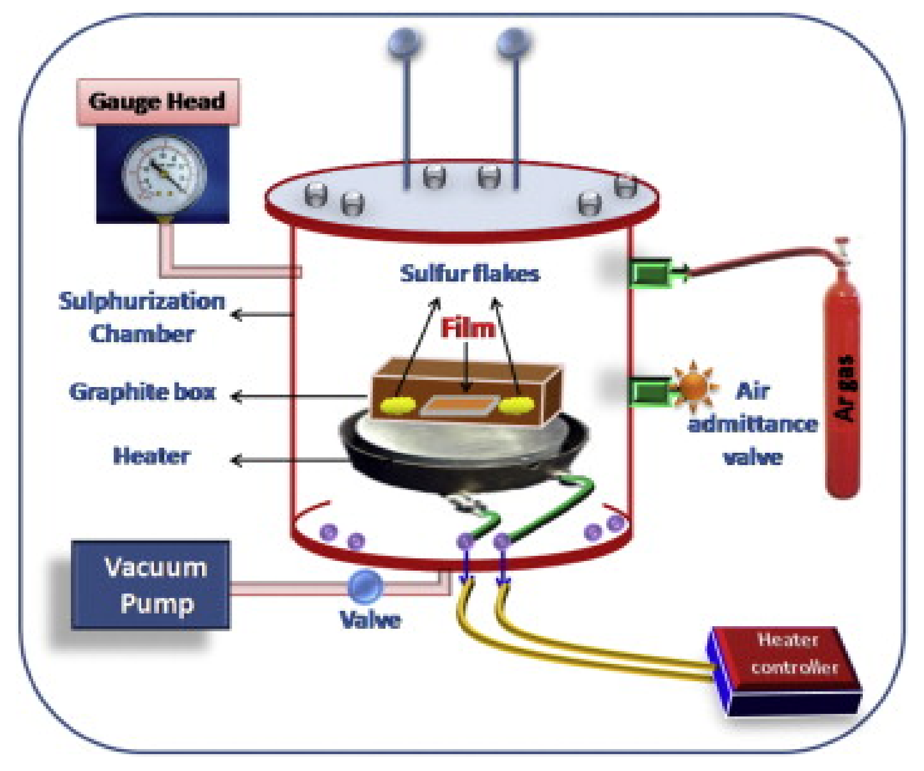
For the deposition of tin (II) monosulfide films on soda-lime glass (SLG), direct current magnetron sputtering (VRSU048) and sulfurization setup [3] were used. First, the base pressure of 1 × 10⁻⁶ Torr was achieved in the chamber of a sputtering system using turbomolecular and rotary pumps. By allowing the argon gas, working pressure of 5 × 10⁻³ Torr was achieved in the chamber of a sputtering system to deposit the metallic tin precursor layers on soda-lime glass. Tin precursor layers were deposited with the tin target (4N, Kurt J. Lesker, UK). The deposited tin precursor layers and sulfur flacks were loaded in a graphite box, which was kept in the sulfurization chamber, as shown in Figure 1. A rotary pump is used to achieve 1 × 10⁻³ Torr. Next, sulfurization was performed in the period of 30–180 min for a fixed sulfurization temperature of 350 °C. The deposition and characterization details were provided in our previous work [3,5,17].

Figure 1.
Experimental setup of the sulfurization (reprinted with permission from [3]; Copyright© 2015 Elsevier Ltd.).
3. Results and Discussion
3.1. XPS Analysis
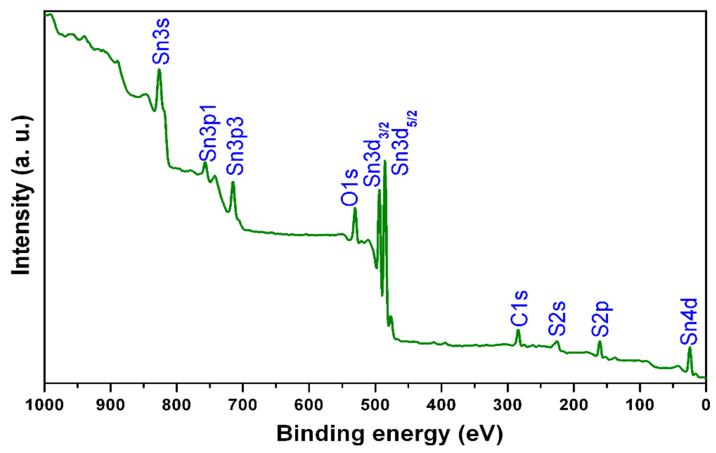
The presence of different elements, their electronic binding energies, and the ionization states of elements in SnS films were investigated by X-ray photoelectron spectroscopy (XPS). The complete scan X-ray photoelectron spectroscopy results are shown in Figure 2 for SnS film sulfurized at a typical time period of 150 min. The binding energy values obtained in the X-ray photoelectron spectroscopy analysis were corrected by referencing the C1s peak to 284.80 eV. The survey X-ray photoelectron spectroscopy of the samples revealed that the presence of tin, sulfur, oxygen, and carbon components. The binding energy (BE) values of the peaks at 485.8 eV and 161.2 eV were assigned to Sn3d5/2 of Sn+2 and S2p3/2 of S−2 in tin (II) monosulfide, respectively [3,18]. Further, Sn0 (at 484.9 eV) and Sn+4 (at 487.3 eV) were not observed in the Sn3d5/2 peak, demonstrating the formation of single-phase tin (II) monosulfide films [19,20,21]. From the XPS analysis, it is confirmed that the tin precursor layers were converted into single-phase tin (II) monosulfide films merely in the entire sulfurization time period. The composition analysis indicated a slightly sulfur-rich composition at lower sulfurization time periods, and with an increase of time period, the composition approaches stoichiometry at 150 min. Thus, the single-phase SnS films had elemental compositions of Sn = 50.2 at% and S = 49.8 at%.
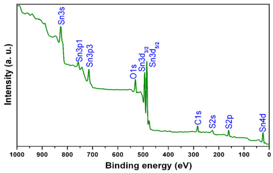
Figure 2.
X-ray photoelectron spectroscopy (XPS) wide scan spectrum of film sulfurized at sulfurization time of 150 min.
3.2. XRD Analysis
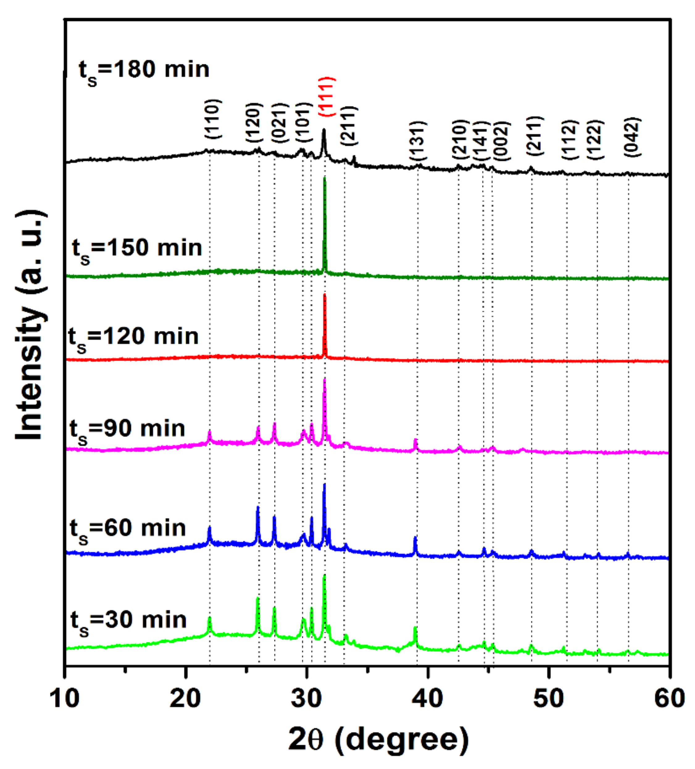
X-ray diffraction (XRD) patterns of tin (II) monosulfide films for various sulfurization durations are shown in Figure 3. It is noticed that all the sulfurized SnS films were polycrystalline in nature. The sulfurized SnS films exhibited an orthorhombic structure. The diffraction peaks present at 2θ values, 22.18°, 26.02°, 26.84°, 29.92°, 31.50°, 31.98°, 33.82°, 38.74°, 42.62°, 44.94°, 45.02°, 48.06°, 52.02°, 54.32°, and 57.46°, can be assigned to the orientations (110), (120), (021), (101), (111), (211), (131), (210), (141), (002), (112), (122), and (042), respectively, of orthorhombic SnS and the data obtained matched well with the standard XRD pattern of SnS (JCPDS: 39-0354 ). The peak intensity and sharpness of (111) orientation increased with the prolonging of ts up to 150 min, and with a further increase of time, the peak intensity decreased. This indicates that the crystallinity of the grown layers was increased with the prolonging of ts up to 150 min, and thereafter, it decreased. The spectra did not show peaks corresponding to other binary tin sulfide phases, namely SnS2 and Sn2S3. From this study, it is concluded that the films were grown exhibited pure SnS phase at all sulfurization times without any secondary phases. The single phase obtained in the present study might be due to the formation of SnS films at the previously optimized sulfurization temperature (350 °C). Jiang et al. [22] also reported the growth of SnS films at different sulfurization times (15, 30, 45, 60 min) using a sulfurization temperature of 220 °C by a two-stage process. However, these films do not exhibit pure SnS phase for all sulfurization time periods, which might be because of a lack of optimization of sulfurization temperature and other parameters. In the literature [23], the films deposited by vacuum techniques showed the preferred orientation of the (111) and (040) planes. In the present case, it is found that, for smaller sulfurization time periods, the films exhibited both (111) and (040) orientations. However, with the extended ts, the intensity of the (040) peak diminished and disappeared after 60 min, whereas the intensity of the (111) peak increased continuously up to a sulfurization time of 150 min, and then decreased slightly.
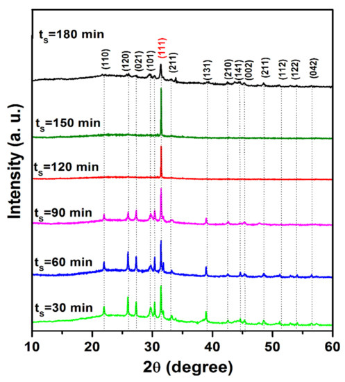
Figure 3.
X-ray diffraction (XRD) patterns of metallic tin precursor films sulfurized at various time periods.
The observed change of tin (II) monosulfide crystal orientation in the present work is due to the surface energies of tin (II) monosulfide crystal planes, which have different energies. Further, tin (II) monosulfide is a layered semiconductor material with the layer plane perpendicular to the b crystallographic axis; the crystal plane of {010} has much lower surface energy than the {100} and {001} crystal plane at the surface boundary. When tin (II) monosulfide starts to nucleate on the substrate surface, the {010} crystal plane would be preferred to align parallel to the substrate to minimize the surface energy. Once the film grows thicker, the surface areas (plane defects) are mainly from the grain boundaries within the film rather than from the top surface. Thus, the minimum surface energy is to have a {010} plane parallel to the grain boundaries, which is perpendicular to the substrate surface owing to the nature of the columnar structure in this case [23]. The preferential orientation of tin (II) monosulfide films is regulated by nucleation, which depends on film thickness, substrate temperature, deposition time, type of substrates, and film preparation method as the process. A similar kind of behavior has also been observed in the earlier studies made by Tanusevski et al. [24] and Cheng et al. [25] in the literature.
The crystallite size of tin (II) monosulfide films is evaluated from the full width at half maxima (FWHM) of the most predominant orientation in the XRD patterns of tin (II) monosulfide films, the (111) plane, using the Scherrer formula [26] given below.
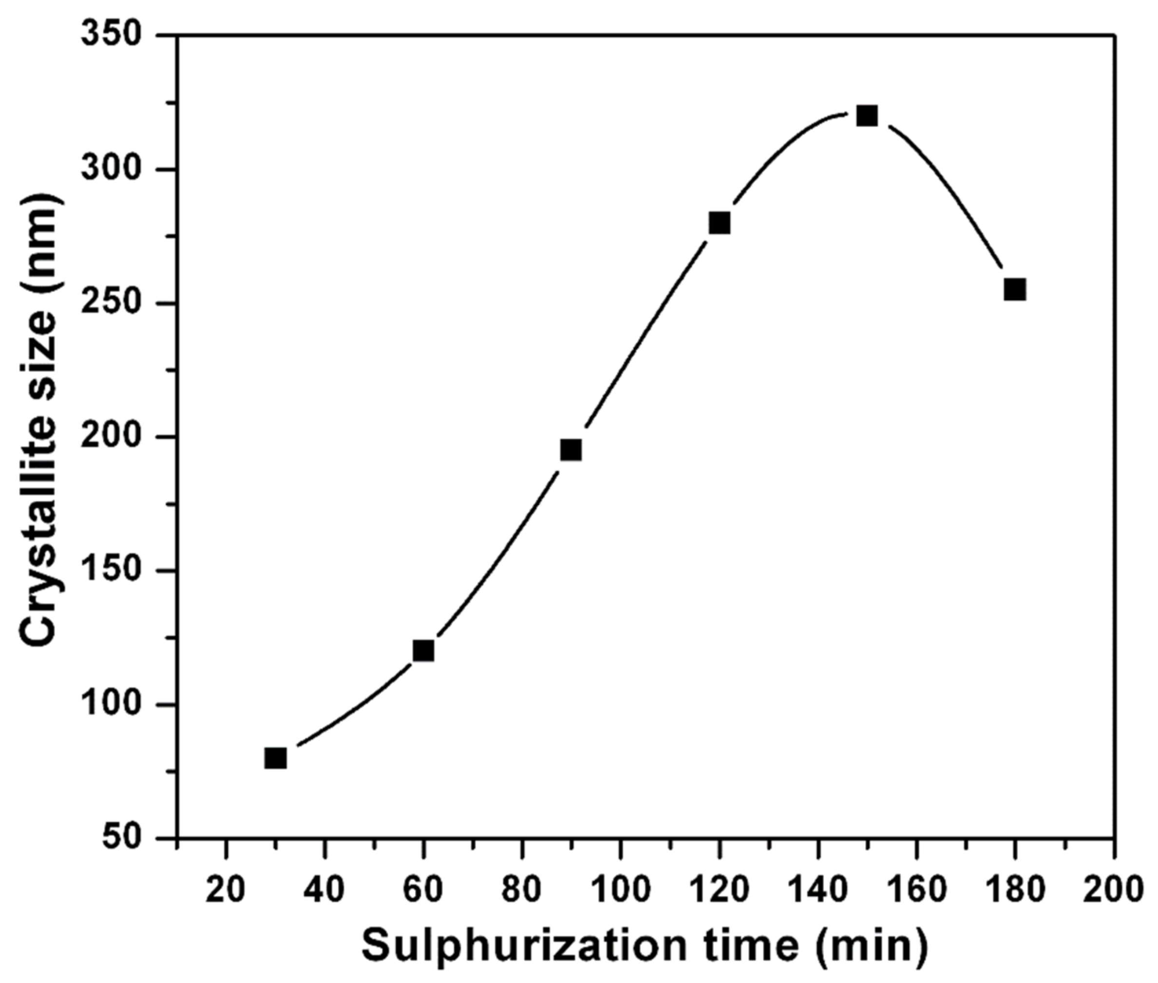
where λ is the radiation wavelength, β is the corrected FWHM of the main X-ray diffraction peak, and θ is the XRD peak position. Figure 4 shows the change of crystallite size with sulfurization time. It can be seen that as ts is prolonged up to 150 min, the crystallite size increased from 80 nm to 320 nm, and then decreased. This is mainly because, with the consistent increase of time (150 min), the recrystallization might take place to improve the crystallite size.

Figure 4.
Variation of crystallite size with sulfurization time.
3.3. Raman Studies
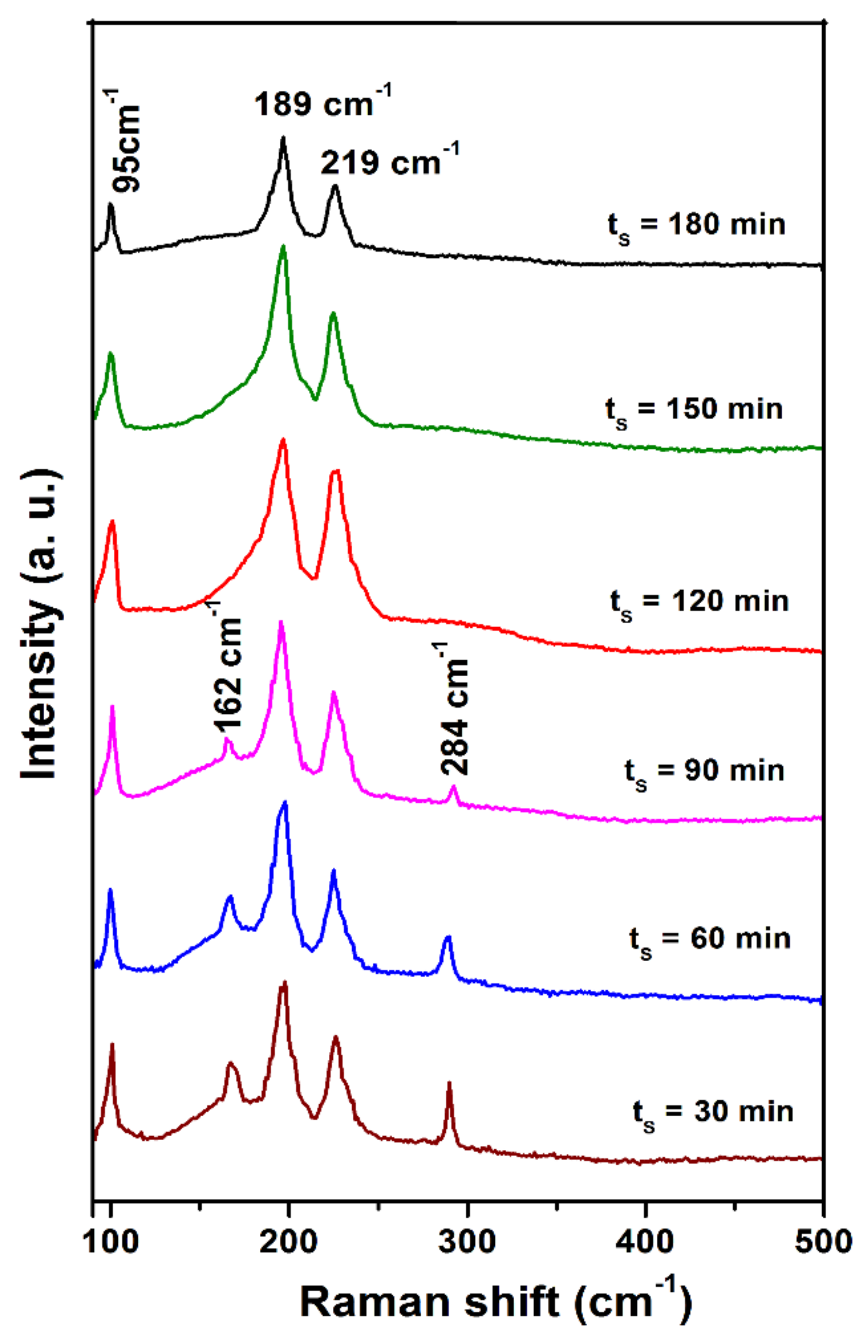
Generally, it is difficult to differentiate the SnS, SnS2, and Sn2S3 using XRD analysis if the films contain a small quantity of these secondary tin sulfide phases. Particularly, differentiation of SnS and Sn2S3 peaks is a great task as the Bragg angles for both peaks fall in the range of 2θ = 31–32° [16]. In this situation, Raman analysis is a straightforward technique to identify the phase purity of SnS. Further, it is also proved to be an important tool for the identification of minor impurities in the case of Cu2ZnSnS4 and Cu2SnS3. Figure 5 shows the Raman spectra of sulfurized films at different sulfurization times, and the spectra were recorded at room temperature. Vibrational modes of sulfurized films were detected at 95 cm−1, 162 cm−1, 189 cm−1, 219 cm−1, and 284 cm−1 for lower than 120 min and 95 cm−1, 189 cm−1, and 219 cm−1 for ≥120 min, related to tin (II) monosulfide. Raman vibrational modes at 95 cm−1, 189 cm−1, and 219 cm−1 belong to the Ag mode of tin (II) monosulfide films, and the other modes at 162 and 284 cm−1 belong to the B2g mode of tin (II) monosulfide films. According to the previous reports, the appearance of Ag and B3g modes of tin (II) monosulfide corresponded to the incident; scattered directions parallel to one of a, b, and c axis of tin (II) monosulfide; and, in the present case, it is the b-axis. Crystal clear B1g and B2g modes of tin (II) monosulfide were not detected; those appeared when the incident scattered direction was parallel to the a-axis and c-axis of tin (II) monosulfide, respectively [27]. In general, owing to dominant electrostatic field interaction in tin (II) monosulfide, the phonons of tin (II) monosulfide exhibit nearly pure longitudinal or transverse character. Mostly, there is no merging that takes place between the transverse and the longitudinal atomic vibrations in tin (II) monosulfide. Under certain propagation and polarization conditions, phonons of combined symmetry character arise and can be detected in the Raman spectra. In the present investigation, the longitudinal optical modes are 162 cm−1, 189 cm−1, 219 cm−1, and 284 cm−1, while the transverse (TO = 3) optical mode is 95 cm−1 [27]. The transverse mode is observed presumably due to the backscattering geometry, which is not strictly backscattering. The results of the present work agree with the previously reported data at vibrational modes of 95 cm−1, 162 cm−1, 189 cm−1, 219 cm−1, and 284 cm−1 for films grown on the amorphous substrate. Further, the intensity of Raman vibrational modes for tin (II) monosulfide films at different sulfurization times is high and sharper with increasing time, indicating the quality of the tin (II) monosulfide films. Furthermore, no significant peak shift and broadening are observed in the Raman spectra, indicating that the films are free from strain. This result confirmed that the films grown at different sulfurization times are single-phase tin (II) monosulfide without the presence of additional phases such as SnS2 (312 cm−1) and Sn2S3 (304 cm−1) [19,28].

Figure 5.
Raman spectra of sulfurized films at various sulfurization durations.
3.4. AFM Studies
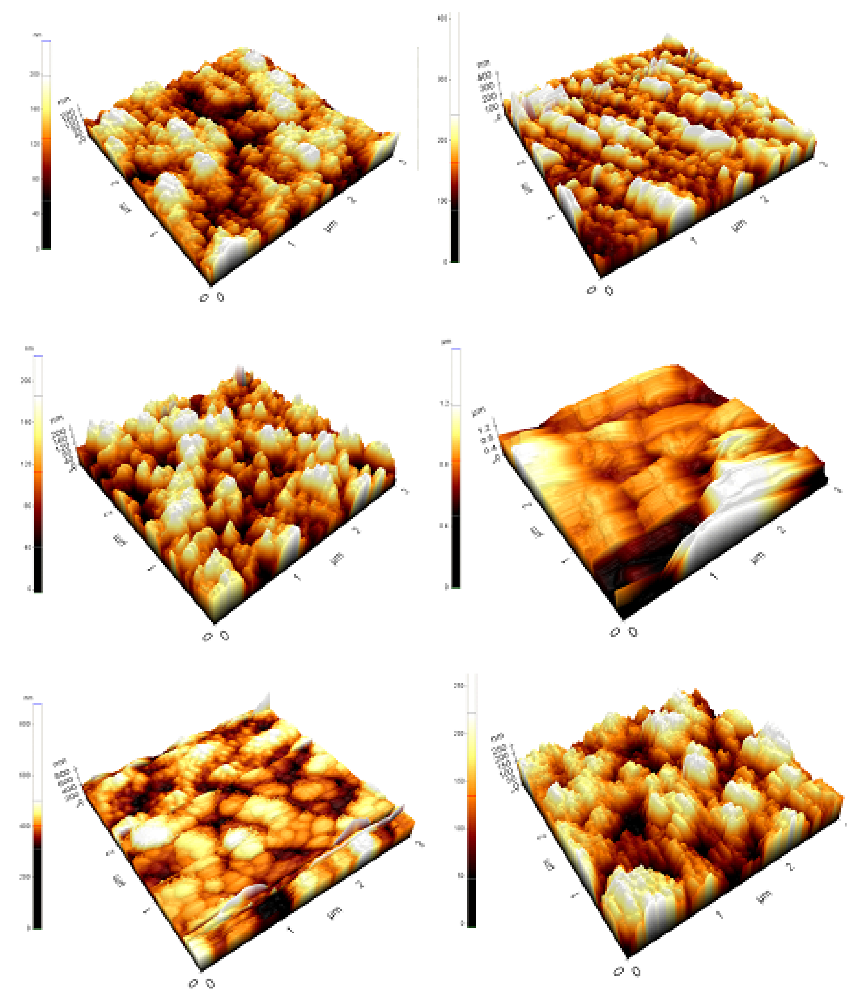
Figure 6 shows the surface topology of tin (II) monosulfide films at various sulfurization times. The roughness of the tin (II) monosulfide films increased with the prolonging of ts, thereby increasing the grain size. The average crystallite size obtained in the XRD results is consistent with AFM studies. The improvement in the crystallinity of the film occurs by the coalescence of the neighboring islands. Further, the films sulfurized at a short sulfurization time had a high surface roughness of 18 nm that decreased to 5 nm when the sulfurization duration was raised further. The average grain size of the films varied in the range of 80–320 nm, with the change of sulfurization time in the range of 30–180 min. The variation in the surface roughness as a function of sulfurization time can be explained as follows. The availability of time to diffuse sulfur atoms into the tin metal layer and filling of sulfur sites could not occur at lower sulfurization times, resulting in the formation of crystallites with higher surface roughness. The formation of polycrystalline SnS thin film can be explained based on the occurrence of a number of events, which are nucleation, growth, and coalescence of islands. As sulfurization time is prolonged, the adsorbed S atoms possess enough sulfurization time to settle on the substrate surface with the minimum potential energy positions (this is cluster or island formation), and the crystallization is facilitated because of island coalescence (growth) promoted by increased surface and volume diffusion of S, resulting in the development of larger grains.

Figure 6.
Atomic force microscope (AFM) images of the SnS films sulfurized at different time periods.
3.5. Optical Studies
To confirm and evaluate the optical properties such as transmittance, absorption coefficient, and bandgap of the sulfurized films, the UV/Vis-NIR transmittance spectra of all the sulfurized films were experimentally measured. Figure 7 shows the transmittance versus wavelength spectra of the films sulfurized at various ts.
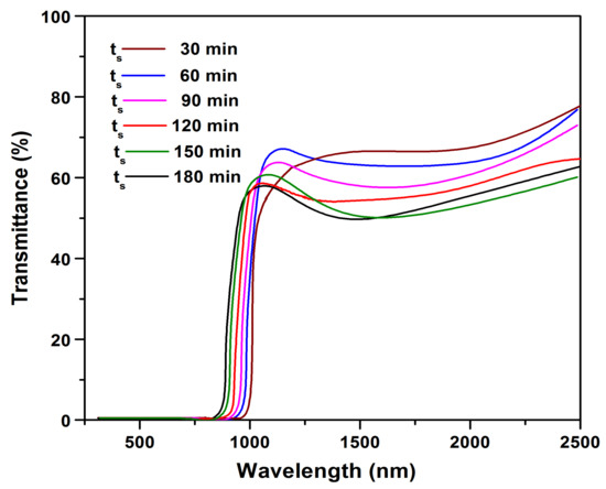
Figure 7.
Transmittance versus wavelength spectra of SnS films.
From Figure 7, a significant change in UV/Vis-NIR transmittance can be noticed with the increase of ts. The films sulfurized at 30 min had higher transmittance, and with the increase in ts to 120 min, the transmittance was found to be decreased, and the absorption edge was blue shifted. With further prolonging the sulfurization time to 150 min, a sharp fall in the fundamental absorption edge was observed. This could be due to the high crystallinity and internal morphology of the sulfurized film.
The absorption coefficient was calculated from the experimentally measured values of transmittance (T) using the following relation [6]:
where t is the thickness of sulfurized films. The evaluated α was in the order of 104 cm−1, which supports the direct bandgap nature of the material. The bandgap of the samples was determined using the following relation [6]:
α = −(1/t) ln(1/T)
αhν = A (hν−Eg)x
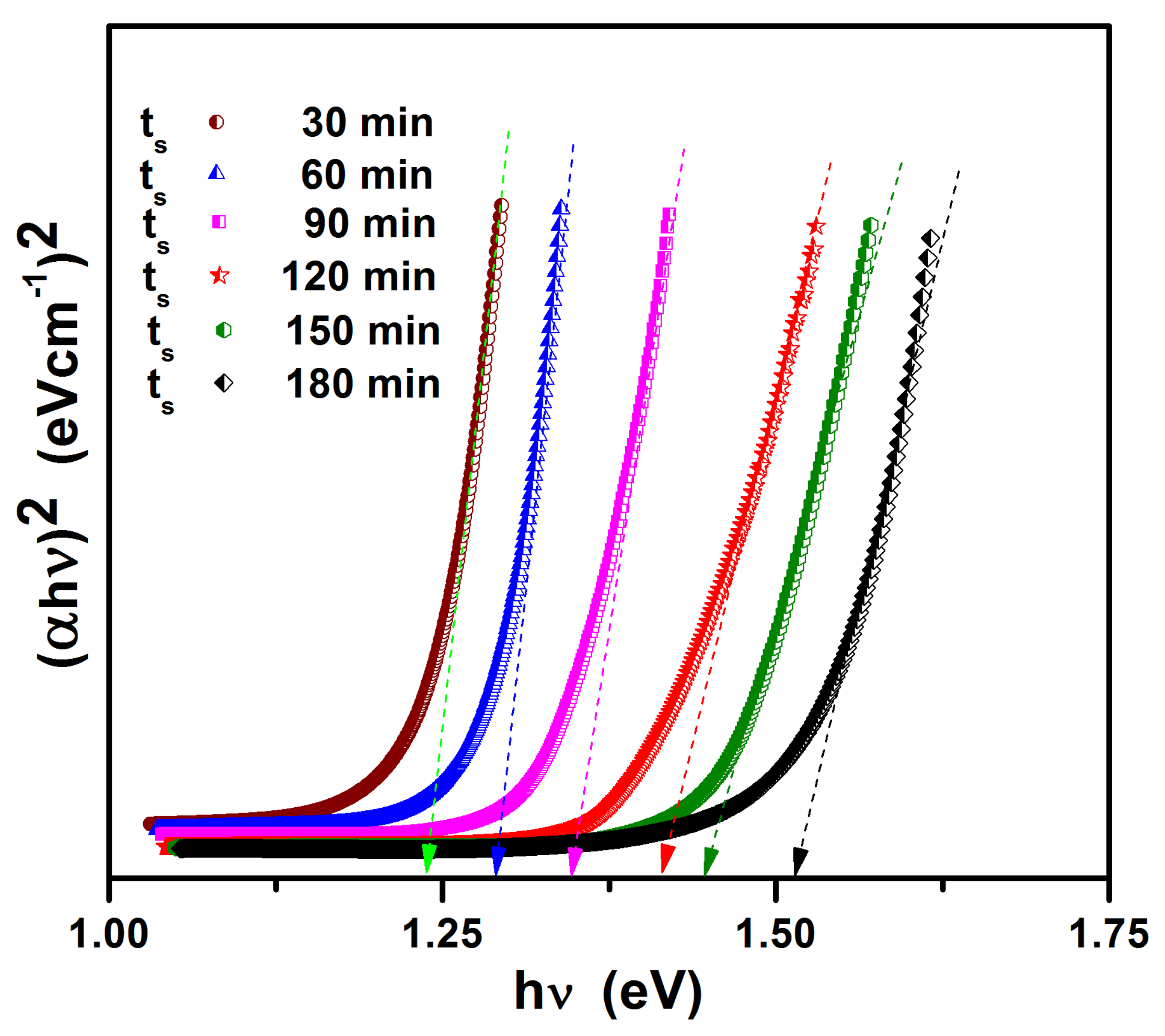
The optical bandgap of sulfurized films is obtained by extrapolating the linear part of the curves onto the horizontal axis. Figure 8 shows the plot of (αhν)2 versus hν for sulfurized films. As seen from the figure, the bandgap increased with ts. The bandgap of the tin (II) monosulfide films increased with the increase in sulfurization time. This is because of the decrease in defect concentration. From the figure, it was observed that, with increasing sulfurization time of tin (II) monosulfide film, the bandgap increases from 1.25 eV to 1.50 eV. This may be because of the change in inhomogeneity and crystallinity of the films. The bandgap of the SnS film is quite close to the optimum bandgap required for a solar cell.

Figure 8.
Plots of (αhν)2 versus hν for SnS films.
4. Conclusions
The SnS films were prepared via a two-stage process using sputtered Sn precursors in the presence of sulfur vapor to study the effect of sulfurization time, which varied in the range of 30–180 min at an optimized sulfurization temperature of 350 °C. The films grown were characterized using structural, topographical, compositional, and optical properties. The XPS spectrum of sulfurized films showed the presence of tin and sulfur. The XRD results revealed that all the tin (II) monosulfide films at different ts were polycrystalline in nature with an orthorhombic structure. It was found that a 30 min of sulfurization time is sufficient for the formation of single phase SnS. The crystallinity of the sulfurized films initially increased with the increase in ts up to 150 min, and tthen decreased. The Raman spectra of tin (II) monosulfide films showed modes at 95, 162, 189, 219, and 284 cm−1 for tS < 120 min and 95, 189, and 219 cm−1 for tS ≥ 120 min. Raman modes present at 95, 189, and 219 cm−1 belong to the Ag (strong) mode, and the other modes at 162 and 284 cm−1 belong to the B2g (weak) mode of SnS. From the transmittance spectra of the sulfurized films, it is clear that the film grown at 30 min had higher transmittance, and with the increase in ts to 120 min, the transmittance was decreased. The optical bandgap of sulfurized films changed in the range of 1.25–1.50 eV. From the above observations, crystallinity can be improved with the optimization of sulfurization time.
Author Contributions
Conceptualization, V.R.M.R.; methodology, V.R.M.R.; formal analysis, S.G.; investigation, V.R.M.R.; data curation, S.G., R.U.A. and V.R.M.R.; writing—original draft preparation, V.R.M.R.; writing—review and editing, K.T.R.R.; supervision, K.T.R.R.; project administration, K.T.R.R. and C.P.; funding acquisition, K.T.R.R., W.K.K. and C.P. All authors have read and agreed to the published version of the manuscript.
Funding
This research received no external funding.
Institutional Review Board Statement
Not applicable.
Informed Consent Statement
Not applicable.
Data Availability Statement
Data available on request due to restrictions e.g., privacy or ethical.
Acknowledgments
This work was supported by “Human Resources Program in Energy Technology” of the Korea Institute of Energy Technology Evaluation and Planning (KETEP), granted financial resource from the Ministry of Trade, Industry, and Energy, Republic of Korea. (No. 20204010600100).
Conflicts of Interest
The authors declare no conflict of interest.
References
- Kushiya, K. CIS-based thin-film PV technology in solar frontier K.K. Sol. Energy Mater. Sol. Cells 2014, 122, 309–313. [Google Scholar] [CrossRef]
- Avrutin, V.; Izyumskaya, N.; Morko, H. Semiconductor solar cells: Recent progress in terrestrial applications. Superlattices Microstruct. 2011, 49, 337–364. [Google Scholar] [CrossRef]
- Vasudeva Reddy, M.; Sreedevi, G.; Chinho, P.; Miles, R.W.; Ramakrishna Reddy, K.T. Development of sulphurized SnS thin film solar cells. Curr. Appl. Phys. 2015, 15, 588–598. [Google Scholar] [CrossRef]
- Gedi, S.; Reddy, V.R.M.; Park, C.; Chan-Wook, J.; Ramakrishna Reddy, K.T. Comprehensive optical studies on SnS layers synthesized by chemical bath deposition. Opt. Mater. Amst. 2015, 42, 468–475. [Google Scholar] [CrossRef]
- Gedi, S.; Minnam Reddy, V.R.; Kotte, T.R.R.; Park, Y.; Kim, W.K. Effect of C4H6O6 concentration on the properties of SnS thin films for solar cell applications. Appl. Surf. Sci. 2019, 465, 802–815. [Google Scholar] [CrossRef]
- Sreedevi, G.; Vasudeva Reddy, M.; Babu, P.; Chan-Wook, J.; Chinho, P.; Ramakrishna Reddy, K.T. A facile inexpensive route for SnS thin film solar cells with SnS2 buffer. Appl. Surf. Sci. 2016, 372, 116–124. [Google Scholar] [CrossRef]
- Vasudeva Reddy, M.; Sreedevi, G.; Babu, P.; Ramakrishna Reddy, K.T.; Guillaume, Z.; Chinho, P. Influence of different substrates on the properties of sulfurized SnS films. Sci. Adv. Mater. 2016, 8, 247–251. [Google Scholar] [CrossRef]
- Nwofe, P.A.; Reddy, K.T.R.; Miles, R.W. Influence of Deposition Time on the Properties of Highly-Oriented SnS Thin Films Prepared Using the Thermal Evaporation Method. Adv. Mater. Res. 2012, 602–604, 1409–1412. [Google Scholar] [CrossRef]
- Nwofe, P.A.; Reddy, K.T.R.; Miles, R.W. Type conversion of p-SnS to n-SnS using a SnCl4CH3OH heat treatment. In Proceedings of the 2013 IEEE 39th Photovoltaic Specialists Conference, Tampa, FL, USA, 16–21 June 2013; pp. 2518–2523. [Google Scholar] [CrossRef]
- Mariappan, R.; Ragavendar, M.; Ponnuswamy, V. Structural and optical characterization of SnS thin films by electro-deposition technique. Opt. Appl. 2011, 41, 989–997. [Google Scholar]
- Ricica, T.; Strizik, L.; Dostal, L.; Bouska, M.; Vlcek, M.; Benes, L.; Wagner, T.; Jambor, R. SnS and SnS2 thin films deposited using a spin-coating technique from intramolecularly coordinated organotin sulfides. Appl. Organomet. Chem. 2015, 29, 176–180. [Google Scholar] [CrossRef]
- Sajeesh, T.H.; Poornima, N.; Sudha Kartha, C.; Vijayakumar, K.P. Unveiling the defect levels in SnS thin films for photovoltaic applications using photoluminescence technique. Phys. Status Solidi Appl. Mater. Sci. 2010, 207, 1934–1939. [Google Scholar] [CrossRef]
- Xie, H.; Sánchez, Y.; López-Marino, S.; Espíndola-Rodríguez, M.; Neuschitzer, M.; Sylla, D.; Fairbrother, A.; Izquierdo-Roca, V.; Pérez-Rodríguez, A.; Saucedo, E. Impact of Sn (S, Se) Secondary Phases in Cu2ZnSn(S, Se)4 Solar Cells: A Chemical Route for Their Selective Removal and Absorber Surface Passivation. ACS Appl. Mater. Interfaces 2014, 6, 12744–12751. [Google Scholar] [CrossRef]
- Sinsermsuksakul, P.; Sun, L.; Lee, S.W.; Park, H.H.; Kim, S.B.; Yang, C.; Gordon, R.G. Overcoming Efficiency Limitations of SnS-Based Solar Cells. Adv. Energy Mater. 2014, 4, 1400496. [Google Scholar] [CrossRef]
- Schneikart, A.; Schimper, H.J.; Klein, A.; Jaegermann, W. Efficiency limitations of thermally evaporated thin-film SnS solar cells. J. Phys. D. Appl. Phys. 2013, 46. [Google Scholar] [CrossRef]
- Banai, R.E.; Horn, M.W.; Brownson, J.R.S. A review of tin (II) monosulfide and its potential as a photovoltaic absorber. Sol. Energy Mater. Sol. Cells 2016, 150, 112–129. [Google Scholar] [CrossRef]
- Minnam Reddy, V.R.; Lindwall, G.; Pejjai, B.; Gedi, S.; Kotte, T.R.R.; Sugiyama, M.; Liu, Z.K.; Chinho, P. α-SnSe thin film solar cells produced by selenization of magnetron sputtered tin precursors. Sol. Energy Mater. Sol. Cells 2018, 176, 251–258. [Google Scholar] [CrossRef]
- Ahmet, I.Y.; Hill, M.S.; Johnson, A.L.; Peter, L.M. Polymorph-Selective Deposition of High Purity SnS Thin Films from a Single Source Precursor. Chem. Mater. 2015, 27, 7680–7688. [Google Scholar] [CrossRef] [Green Version]
- Joshi, M.P.; Khot, K.V.; Patil, S.S.; Mali, S.S.; Hong, C.K.; Bhosale, P.N. Investigating the light harvesting capacity of sulfur ion concentration dependent SnS 2 thin films synthesized by self-assembled arrested precipitation technique. Mater. Res. Express 2019, 6, 086467. [Google Scholar] [CrossRef]
- Calderón Triana, C.L.; Banguero, E.; Bartolo-Pérez, P.; Gordillo, G. Preparation and Characterization of SnS:Bi Thin Films. Braz. J. Phys. 2011, 41, 15–20. [Google Scholar] [CrossRef]
- Jing, L.; Xu, Y.; Zhang, M.; Xie, M.; Xu, H.; He, M.; Liu, J.; Huang, S.; Li, H. Novel Ag2S quantum dot modified 3D flower-like SnS2 composites for photocatalytic and photoelectrochemical applications. Inorg. Chem. Front. 2018, 5, 63–72. [Google Scholar] [CrossRef]
- Jiang, F.; Shen, H.; Gao, C.; Liu, B.; Lin, L.; Shen, Z. Preparation and properties of SnS film grown by two-stage process. Appl. Surf. Sci. 2011, 257, 4901–4905. [Google Scholar] [CrossRef]
- Sinsermsuksakul, P.; Heo, J.; Noh, W.; Hock, A.S.; Gordon, R.G. Atomic layer deposition of tin monosulfide thin films. Adv. Energy Mater. 2011, 1, 1116–1125. [Google Scholar] [CrossRef] [Green Version]
- Tanusevski, A. Optical and photoelectric properties of SnS thin films prepared by chemical bath deposition. Semicond. Sci. Technol. 2003, 18, 501–505. [Google Scholar] [CrossRef]
- Cheng, S.; He, Y.; Chen, G.; Cho, E.C.; Conibeer, G. Influence of EDTA concentration on the structure and properties of SnS films prepared by electrodeposition. Surf. Coat. Technol. 2008, 202, 6070–6074. [Google Scholar] [CrossRef]
- Chaki, S.H.; Deshpande, M.P.; Trivedi, D.P.; Tailor, J.P.; Chaudhary, M.D.; Mahato, K. Wet chemical synthesis and characterization of SnS2 nanoparticles. Appl. Nanosci. 2013, 3, 189–195. [Google Scholar] [CrossRef] [Green Version]
- Lu, F.Y.; Yang, J.H.; Li, R.X.; Huo, N.J.; Li, Y.T.; Wei, Z.M.; Li, J.B. Gas-dependent photoresponse of SnS nanoparticles-based photodetectors. J. Mater. Chem. C 2015, 3, 1397–1402. [Google Scholar] [CrossRef]
- Banu, S.; Ahn, S.J.; Eo, Y.J.; Gwak, J.; Cho, A. Tin monosulfide (SnS) thin films grown by liquid-phase deposition. Sol. Energy 2017, 145, 33–41. [Google Scholar] [CrossRef]

Publisher’s Note: MDPI stays neutral with regard to jurisdictional claims in published maps and institutional affiliations. |
© 2021 by the authors. Licensee MDPI, Basel, Switzerland. This article is an open access article distributed under the terms and conditions of the Creative Commons Attribution (CC BY) license (https://creativecommons.org/licenses/by/4.0/).