1. Introduction
Infrared photodetectors, as an indispensable bridge for the transformation of optical signals into electrical signals, have been widely used in various technical fields [
1,
2,
3,
4]. In practical applications, the detector is often placed on the focal of the optical receiving system to achieve efficient absorption of light energy. However, after the photodetector absorbs light energy, its temperature rises, greatly affecting its performance. When the detector surface temperature increases, the dark current of the device will increase, thus the signal noise ratio will decrease, and the detection effect of the pairing signal will be affected. When the surface temperature of the detector increases further, it may cause soft damage or hard damage to the detector. Therefore, it is necessary to research the thermal characteristics of the detector. Kruer and Bartoli established a thermal model for polycrystalline lead sulfide (PbS), polycrystalline lead selenide (PbSe), and mercury cadmium telluride (HgCdTe) infrared (IR) detectors [
5,
6]. Among numerous kinds of detectors, APDs have the unique advantages of small size, high sensitivity, and the ability to work at room temperature. They are thus employed in various fields [
7,
8,
9,
10], especially in the field of laser detection, where they are most widely used. However, to date, there have been few studies on the new physical phenomena when an APD is irradiated by a millisecond pulse laser. In 2015, with the use of a 1064 nm pulse laser, the characteristics of an irradiated avalanche photodiode were studied [
11]. Our research group has studied the temperature rise characteristics of a millisecond pulse laser interacting with a Si-APD and the capacitance–voltage curve of the damaged Si-APD under the condition of no external capacitance. The research results show that Joule heating plays a significant role when the Si-APD is irradiated by a ms pulse laser [
12]. In this study, based on previous research, an experimental study on the interaction between the millisecond pulse laser and the Si-APD in an external capacitor circuit was carried out. It was firstly found that the maximum surface temperature of the Si-APD decreases significantly with a decrease in external capacitance. An explanation is given from the point of view of carrier transport. The existence of external capacitance has a certain blocking effect on the carrier inside the detector. With the capacitor charging process, the carrier transportability becomes weaker and weaker, and the current density inside the PN junction decreases in an exponential form. When the capacitor is fully charged, the circuit is open, and carrier transport process stops. Moreover, the smaller the capacitance value of the external capacitor, the easier it is to fill with charge, and the stronger the hindrance to the transport capacity of the carrier. The results of this research can be used to guide the design of infrared laser detection circuits. The research results have a certain practical significance for the damage and protection of mid-infrared detectors [
13,
14]. By optimizing the value of capacitance in the driving circuit, the anti-damage ability of the infrared detector towards mid-infrared lasers generated by a periodically polarized crystal can be further improved. When the detector surface temperature increases, the dark current of the device will increase, and thus the signal to noise ratio will decrease, and the detection effect of the pairing signal will be affected. When the surface temperature of the detector increases further, it may cause soft damage or hard damage to the detector. Therefore, it is very significant to study the surface temperature rise in the detector under the action of laser irradiation.
2. Materials and Methods
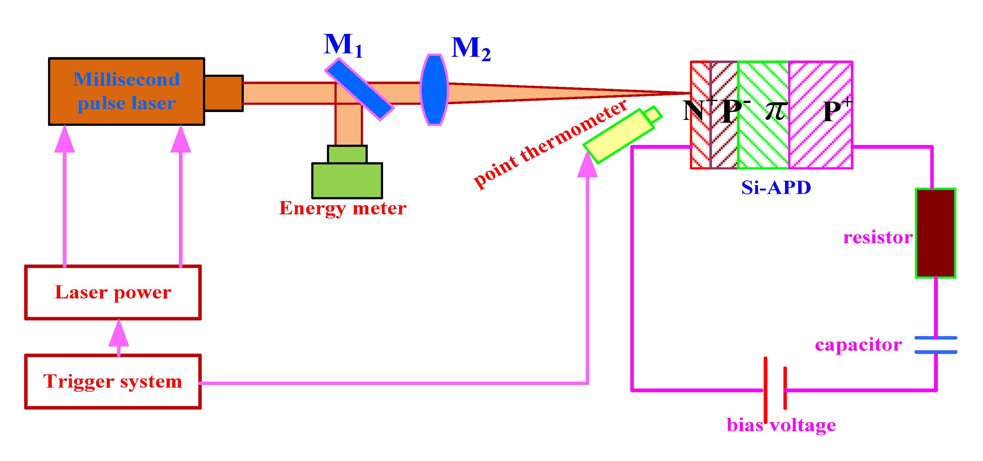
Figure 1 is the experimental device for the measurement of the temperature rise in a Si-APD irradiated by a millisecond pulse laser. The device is mainly composed of a laser system, a point thermometer, and a Si-APD external circuit. A Nd:YAG millisecond pulse laser with a pulse width was 1.0 ms and a wavelength of 1064 nm is used. The laser irradiates the surface of the detector vertically, and the focus is located on the surface of the detector. The point temperature meter and the optical axis of the laser are placed at 45 degrees, which can effectively avoid the influence of the laser on the measurement accuracy of the point temperature meter. The emitted laser beam is divided into two parts by a beam splitter. One part of the laser beams is focused on the APD surface through a lens, the energy of the other part is monitored by an energy meter, and the ratio of laser energy incident on the surface of the Si-APD detector and energy meter is 10:1. The diameter of the focusing spot is 360 μm. The laser and the point temperature meter are triggered by the same trigger, which can ensure that the point temperature meter begins to measure the temperature at the moment when the laser starts to irradiate, to ensure the synchronicity of the laser-irradiated Si-APD and the point temperature meter. In the experiment, we used a laser frequency of 1 Hz. It is simply a one shot–one temperature measure. The Si-APD external circuit is composed of a 180 V-bias voltage source, capacitor, resistor, and Si-APD. In the experiment, 1 μf and 47 pf capacitors were connected in series in the bias circuit. The Si-APD (the commercial specification is Ø800, made in China) used in the experiment was the N + P − πP
+ type, with a layered structure, which is composed of four layers, and the doping distribution and thickness of each layer are different. The doping concentrations of each layer are 5 × 10
19 cm
−3, 5 × 10
16 cm
−3, 5 × 10
12 cm
−3, and 1 × 10
19 cm
−3. The corresponding thicknesses are 1 μm, 3 μm, 50 μm, and 250 μm.
3. Results
The classical heat conduction process can be expressed as follows [
15,
16]:
where
, C, and
k are the material density, specific heat, and heat conductivity, respectively. When the Si-APD is placed in the reverse bias circuit and irradiated by the millisecond pulse laser, the heat source term is improved as the sum of the laser heat source outside the detector and the Joule heat source inside the detector, and the equation can be expressed as:
Finally, the following equation can be derived:
The expression of laser heat is:
E and
τ are the pulse energy and pulse width of the laser, respectively.
,
,
are the absorption coefficients of silicon, the reflection coefficient of silicon, and the time distribution of the laser beam, respectively. The expression of Joule heat is:
When the pulse width is 1.0 ms, energy density is 15 J/cm
2, and theoretical and experimental temperature rise characteristics of the Si-APD in different capacitor driving circuits are shown as
Figure 2. Additionally, the system parameters used in the theoretical simulation are as follows:
330 − 2.19
10
−2 T (kg
m
−3), specific heat
C = 352.43 + 1.78
T − 2.21
10
−2 T2 + 1.3
10
−6 T3 − 2.83
10
−10 T4 (J
kg
−1),
k = 22.23 + 422.52
exp(−
T/255.45) (W
m
−1−1).
The results show that the temperature change in the Si-APD surfaces can be divided into rapid rise stage, plateau stage, and temperature drop stage. This is because, at the beginning of the laser action, the Si-APD is heated not only by the incident laser, but also by the Joule heat, that is to say, the dual heat sources are working together.
The temperature rise in the Si-APD increases the Joule heat, and the increase in the Joule heat further intensifies the temperature rise. In this way, the surface temperature and internal Joule heat of the Si-APD are mutually iterative, and the surface temperature of the Si-APD increases rapidly in a short time at the beginning of laser irradiation. However, according to the theory of semiconductor physics, when the temperature of the PN junction is more than 520 K, the characteristics of the semiconductor will fail, and the Joule heat in the PN junction will disappear. Therefore, only a single laser source can heat the Si-APD. Under the action of heat conduction, the surface temperature of the Si-APD rises slowly and enters a plateau stage. At the end of the laser action, all heat sources disappear, and the surface temperature decreases rapidly under the action of heat conduction. At the same time, we can also see that the temperature rise is significantly affected by different external capacitors. With the decrease in capacitance, the surface temperature of the Si-APD decreases. This observation shows that the surface temperature of the Si-APD is strongly dependent on the external capacitance.
Based on the study of the temperature rise process under different external capacitance conditions, the maximum temperature rise in the Si-APD surface under different external capacitance conditions was investigated by changing the laser energy density. The experimental results are shown in
Figure 3.
As shown in the figure, when the laser energy density is constant, the maximum value of the temperature rise without a capacitance is higher than that with a capacitance. When the driving circuit is connected with different capacitors, the maximum temperature rise will be significantly affected. The smaller the capacitance in the driving circuit, the lower the maximum temperature rise on the detector surface. That is to say, the maximum temperature rise on the detector surface is inversely proportional to the capacitance value. To better understand this, we studied the mechanism by analyzing the carrier transport process.
Figure 4 shows the internal mechanism for the influence of the different capacitances on the maximum surface temperature rise in the Si-APD. The case without capacitance is shown in
Figure 4a, the barrier between PN junctions in the Si-APD is highest under the action of a reverse bias voltage, and a high electric field intensity area is generated in the depletion layer. When the millisecond pulse laser irradiates the Si-APD, the photocarriers generated in the Si-APD are swept away rapidly under the action of high electric field intensity, which results in a large transient current. As Joule heat is the product of electric field intensity and current density, more Joule heat will be generated in the Si-APD when the electric field strength and current density become large simultaneously. However, when a capacitor is connected in series in the circuit, the charges in the circuit will gradually accumulate on both sides of the capacitor plate, hindering the current in the circuit. In this way, the photogenerated carriers in the Si-APD cannot flow into the external circuit smoothly. The carriers accumulate on both sides of the PN junction, forming an additional potential that is opposite to the original potential. This additional potential and the original potential cancel each other out due to the opposite direction, resulting in a decrease in the internal total electric field. Thus, the current density and electric field intensity decrease simultaneously, which reduces the Joule heat. At the same time, it can be seen from
Figure 4b,c that the smaller the external capacitance, the weaker its ability to store charges, thus the stronger its ability to block the current in the circuit. At this time, a larger additional potential is formed on both sides of the PN junction, which makes the current density and electric field inside the Si-APD smaller, resulting in less Joule heat. In other words, the Joule heat inside the Si-APD is positively proportional to the capacitance. Therefore, the maximum surface temperature rise in the Si-APD decreases with the decrease in capacitance in the circuit.
4. Conclusions
In conclusion, the temperature rise characteristics of the interaction between a millisecond pulse laser and the Si-APD in a capacitor circuit have been studied theoretically and experimentally. The results show that the Joule heat is only produced in a very short time at the beginning of laser action, so the surface temperature change process of a Si-APD under different capacitances can be divided into three stages: rapid heating period, plateau period, and falling period. Under the condition of the same laser parameters and different capacitors, the maximum surface temperature rise in the Si-APD has a significant dependence on the external capacitance, which mainly shows that the maximum temperature rise is smaller with a decrease in capacitance. This result is mainly because the existence of capacitance hinders the generation of photogenerated current in the Si-APD, and with the decrease in capacitance, the blocking effect is more significant. This effect causes the carriers to accumulate on both sides of the PN junction to form an additional potential opposite to the original potential, which reduces the internal field strength of the Si-APD and weakens the Joule heat generation. The results suggest that in the design of a laser detection circuit for APD, the selection of capacitance should not only involve consideration of the filtering effect, but also its influence on the temperature rise characteristics of the Si-APD. In the following experiments, a point temperature meter and multi-spectral temperature meter will be used to measure the temperature jointly, to further improve the accuracy of temperature measurement. This could lay a solid data foundation for further research on the mechanism of the detector surface temperature rise under the action of laser irradiation.

