1. Introduction
As the main input port of detection and measurement systems, photodetectors have been widely used in optical tomography, communication, radar and other technical fields [
1,
2]. Compared to other detectors, an avalanche photodiode (APD) has the advantages of a high quantum efficiency, so this photodetector has been used most widely [
3,
4,
5,
6]. The multi-pulse 1064-nm laser that irradiated APD was researched, and the results showed that a multi-pulse did not affect the damage threshold when the repetition frequency was less than 1Hz; however, when the repetition frequency was greater than 1 Hz, the damage threshold decreased with an increase of the number of pulses [
7]. In 2015, Koronnov A. A. et al. studied the characteristics of germanium avalanche photodiodes irradiated by a high-powered laser using a 4-ns pulse width and 1.064-um wavelength pulse laser [
8]. The experimental and theoretical investigations of millisecond pulse laser ablation-biased Si avalanche photodiodes were studied, and the mechanisms of the phenomenon were studied experimentally and theoretically [
9]. The C–V curve of Si-APD was obtained by using a semiconductor analyzer when the millisecond pulse laser was irradiating [
10]. This research mainly focused on the research of laser damage to APD, and the law of the change of the photocurrent and the carrier transport behavior in APD and the potential barrier between the PN junctions have not been studied. When APD is used as a laser detection element, it converts the photogenerated current into a voltage signal through a load resistor. Therefore, it is of great significance to study the characteristics of the photocurrent and the mechanism of photocurrent generation when a pulsed infrared laser irradiates APD.
In this paper, the internal mechanism of photocurrent generation in APD irradiated by a millisecond pulse laser is studied for the first time. The microscopic mechanism of the barrier between the carrier and PN junction in APD is studied by the macroscopic representation of the sampling current. With the rapid development of a mid-infrared laser, the detection technology of infrared lasers has gradually attracted people’s attention. The research results of this paper can be extended from the response of the detector to high-powered infrared pulse lasers and provide a certain experimental basis for the design of the millisecond pulse infrared laser detection circuit.
2. Materials and Methods
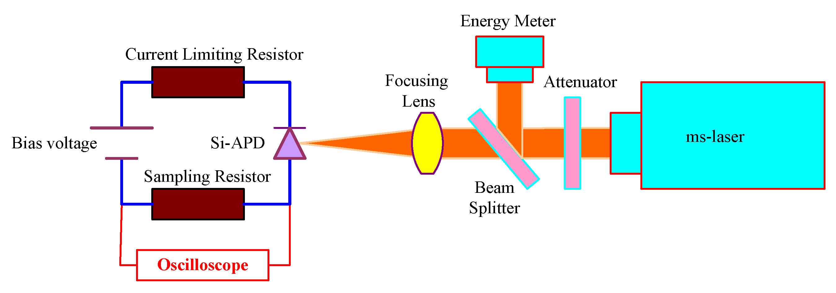
The experimental arrangement is shown schematically in
Figure 1. The wavelength of the millisecond laser is 1064 nm (the laser was self-developed by our research group, and the pulse width is 1–5 ms and is tunable), and the pulse repetition rate could be varied manually from 1 Hz to 10 Hz by changing the firing rate of the flash lamp. An attenuator with an attenuation rate of 10 was located at the exit of the laser; the 2:1 Beam:Split was placed after the attenuator. The TEM00 mode laser beam was focused by a lens with a 20-cm focal length. The beam spot size determined by the slit-scan technique was of the order of 360 μm at the focal spot and was independent of the pulse repetition rate, and the error of the spot size was about 5% [
11,
12]. The Si-APD was biased with 180 V when it was irradiated by the millisecond pulse laser.
The test samples were Si-APDs with the reach-through structure shown in
Figure 2. The surfaces of these detectors are coated with a standard antireflection film, and the active area is 0.5 mm
2.
The experimental system consists of a sampling resistor, current limiting resistor, Si-APD, high-voltage DC power supply, oscilloscope, etc., of which the sampling resistance is 50 KΩ, the current limiting resistor is 1 MΩ and the working voltage is 180 V. The sample is a drawing-type silicon-based APD detector, which is mainly composed of four layers of N+–P−–π–P+. When a higher reverse bias voltage is applied to the outside, the depletion region passes through and reaches the P+ region, and the reverse bias voltage, which exceeds the multiplication voltage, falls all in the π-region; moreover, the collision ionization occurs when the carrier is in the high field region, and they can obtain a sufficiently high average velocity. Since the π-region is much wider than the P-region, the field intensity in the high field region (P-region) and the multiplication rate of the carrier, which are above the avalanche voltage, increase slowly with the reverse bias. Under the working conditions, although the electric field in the π-region is much weaker than in the high field region (P-region), it is sufficient to keep the carrier at a certain drift velocity and transit the π-region in a short time. The faster the carrier drifts, the shorter the transit time is, and the more avalanche ionization occurs when entering the P-region.
3. Results and Discussion
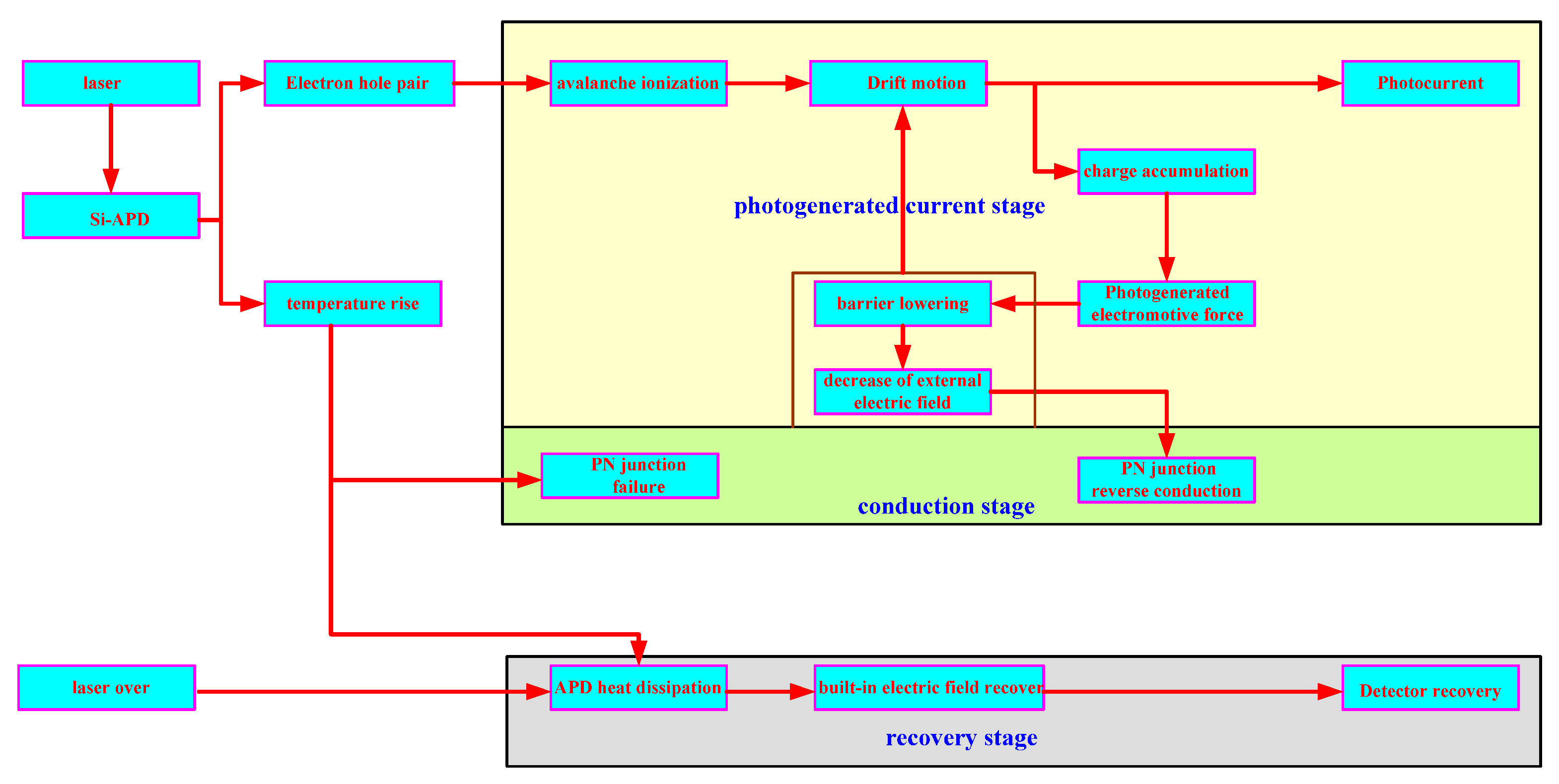
Figure 3 shows that the sampling current with time is divided into three stages: the photogenerated current stage, conduction stage and recovery stage. During the first stage, the peaks of the photocurrent are decreased while the laser energy density increases, and the peak time is basically the same. However, in the conduction stage, the photocurrent is a constant under the action of a laser with different energy densities, and its value depends on the external resistance. In the recovery phase, the recovery time increases with the increase of the laser energy density.
The reason for this phenomenon can be explained as follows: with the increasing of the laser energy density, the number of photogenerated electron–hole pairs increased in the π-region, owing to the action of the π-region electric field, the photogenerated carriers, which resulted from avalanche ionization that swept fast into the P-region (multiplication region), and then the inverse current, which is the photocurrent generated in the Si-APD. Unfortunately, due to the external resistance limit, not all of the photogenerated carriers can be quickly exported into the external circuit, and the excess carriers are accumulated, which results in the cumulative effect of a charge at both ends of the PN junction. The accumulated charge forms a photomotive electromotive force at both ends of the PN junction, thereby pulling down the built-in electric field of the π and P regions. Thus, the increase of the reverse current is hindered. With the increase of the incident laser light intensity, the number of electron hole pairs increases at the same time, and the photo-generated electromotive force increases in order to further pull down the barrier in the junction area [
13,
14]. The schematic diagram of the barrier change is shown in
Figure 4. That is to say, the decrease of the potential barrier between the PN junctions in APD is the basic reason that the peak value of the photocurrent decreases with the increase of the laser intensity.
As the potential barrier between the PN junctions is further lowered, the external electric field at both ends of APD is further reduced until it is zero and APD is in a reversed-conduction state. At this time, the current flowing through APD is a constant, which is equal to the ratio of voltage and resistance in the external circuit. With the continuous action of the laser, the temperature of APD increases gradually. When the temperature is higher than 500 K, APD will go into a failure state [
15]. At this time, the current flowing through APD is still equal to the ratio of voltage and resistance in the external circuit.
When the laser action is over, APD enters the stage of heat recovery, which is dominated by heat dissipation. With the increase of laser energy density, the temperature in APD needs more time to recover to the initial temperature. During this period, the built-in electric field gradually returns to the original state, and the carriers in APD still form a photocurrent due to the external electric field, which leads to a prolongation of the time when the photocurrent drops to zero. The internal mechanism of generating a photocurrent when a millisecond pulse laser irradiates APD can be explained by the following flowchart, as shown in
Figure 5 [
16].
4. Conclusions
In this paper, the sampling current characteristics of APD irradiated by a millisecond pulse infrared laser were studied, and the internal generation mechanism of the current characteristics was analyzed. It was found that the sampling current can be divided into a photocurrent stage, conduction stage and recovery stage. In the photocurrent generation stage, the peak current decreases with the increase of the laser energy density, which is mainly due to the decrease of the potential barrier between the PN junctions caused by the accumulation of charges at both ends of the PN junctions. When the barrier between PN junctions dropped to zero, the APD turned on in reverse, and the current value is a certain value, which is equal to the ratio of voltage-to-resistance in the external circuit. In the recovery phase, built-in electric field recovery and temperature recovery are carried out simultaneously; thus, the higher the energy density of the incident laser, the longer it takes for the current to fall to zero.
Author Contributions
Conceptualization, L.C. and Z.W.; methodology, Z.W.; software, D.W.; validation, L.C. and G.-Y.J.; formal analysis, Z.W.; investigation, L.C.; resources, L.C.; data curation, D.W.; writing—original draft preparation, L.C.; writing—review and editing, L.C.; visualization, Z.W.; supervision, G.-Y.J. and project administration and funding acquisition, G.-Y.J. All authors have read and agreed to the published version of the manuscript.
Funding
This study received funding from the National Natural Fund Project of China (grant no. 61805024).
Data Availability Statement
The data presented in this study are available upon request from the corresponding author.
Acknowledgments
We thank the Key Laboratory of Jilin Province Solid-State Laser Technology and Application for use of the equipment.
Conflicts of Interest
The authors declare no conflict of interest.
References
- Enne, R.; Steindl, B.; Zimmermann, H. Speed optimized linear-mode high-voltage CMOS avalanche photodiodes with high responsivity. Opt. Lett. 2015, 40, 4400–4403. [Google Scholar] [CrossRef] [PubMed]
- Gaberl, W.; Steindl, B.; Schneider-Hornstein, K.; Enne, R.; Reinhard, H.Z. 0.35 lm CMOS avalanche photodiode with high responsivity and responsivity–bandwidth product. Opt. Lett. 2014, 39, 586–589. [Google Scholar] [CrossRef] [PubMed]
- Ferraro, M.S.; Clark, W.R.; Rabinovich, W.S.; Mahon, R.; Murphy, J.L.; Goetz, P.G.; Thomas, L.M.; Burris, H.R.; Moore, C.I.; Waters, W.D.; et al. InAlAs/InGaAs avalanche photodiode arrays for free space optical communication. Appl. Opt. 2015, 54, F182–F188. [Google Scholar] [CrossRef] [PubMed]
- Mu, Y.; Niedre, M. Fast single photon avalanche photodiode-based time-resolved diffuse optical tomography scanner. Biomed. Opt. Express 2015, 6, 3596–3609. [Google Scholar] [CrossRef] [PubMed] [Green Version]
- Nada, M.; Kanazawa, S.; Yamazaki, H.; Nakanishi, Y.; Kobayashi, W.; Doi, Y.; Ohyama, T.; Ohno, T.; Takahata, K.; Hashimoto, T.; et al. High-linearity Avalanche Photodiode for 40-km Transmission with 28-Gbaud PAM4. In Optical Fiber Communication Conference; Optical Society of America: Washington, DC, USA, 2015. [Google Scholar] [CrossRef]
- Nada, M.; Yokoyama, H.; Muramoto, Y.; Ishibashi, T.; Matsuzaki, H. A 50-Gbit/s vertical illumination avalanche photodiode for 400-Gbit/s Ethernet systems. Opt. Express 2014, 22, 14681–14687. [Google Scholar] [CrossRef] [PubMed]
- Arora, V.K.; Dawar, A.L. Laser-induced damage studies in silicon and silicon-based photo detectors. Appl. Opt. 1996, 35, 7061–7065. [Google Scholar] [CrossRef]
- Koronnov, A.A.; Zverev, G.M.; Zemlyanov, M.M. Characteristics of the germanium avalanche photodiode subjected to a high power laser irradiation. Prikl. Fiz. 2015, 4, 54–58. [Google Scholar]
- Wang, D.; Wei, Z.; Jin, G.-Y.; Chen, L.; Liu, H.-X. Experimental and theoretical investigation of millisecond-pulse laser ablation biased Si avalanche photodiodes. Int. J. Heat Mass Transf. 2018, 122, 391–394. [Google Scholar] [CrossRef]
- Yuan, D.; Di, W.; Zhi, W.; Ran, F.T. Study on the inversion of doped concentration induced by millisecond pulsed laser irradiation silicon-based avalanche photodiode. Appl. Opt. 2018, 57, 1051–1055. [Google Scholar] [CrossRef] [PubMed]
- Anoop, G.; Milster, T.D. Spot distribution measurement using a scanning nanoslit. Appl. Opt. 2011, 50, 4746–4754. [Google Scholar]
- Fair, R.B. A wide slit scanning method for measuring electron and ion beam profiles. J. Phys. E Sci. Instrum. 1971, 4, 35–36. [Google Scholar] [CrossRef]
- Brennan, K.F. The Physics of Semiconductors; Cambridge University Press: Cambridge, MA, USA, 1999. [Google Scholar]
- Selberherr, S. Analysis and Simulation of Semiconductor Devices; Springer: New York, NY, USA, 1984. [Google Scholar]
- En-Ke, L.; Bing-Sheng, Z.; Jin-Sheng, L. The Physics of Semiconductors; Electronics Industry: Beijing, China, 2011. [Google Scholar]
- Neamen, D.A. Semiconductor Physics and Devices: Basic Principles; The McMGraw-Hill Education: New York, NY, USA, 2012. [Google Scholar]
| Publisher’s Note: MDPI stays neutral with regard to jurisdictional claims in published maps and institutional affiliations. |
© 2021 by the authors. Licensee MDPI, Basel, Switzerland. This article is an open access article distributed under the terms and conditions of the Creative Commons Attribution (CC BY) license (https://creativecommons.org/licenses/by/4.0/).

