Article

Effect of Thickness of InP Nucleation Layer on the Two-Step Growth of InP on Si(001)

1
The State Key Discipline Laboratory of Wide Band Gap Semiconductor Technology, School of Microelectronics, Xidian University, Xi’an 710071, China
2
China Electronic Product Reliability and Environment Testing Research Institute, Guangzhou 511370, China
*
Authors to whom correspondence should be addressed.
Crystals 2022, 12(4), 462; https://doi.org/10.3390/cryst12040462
Submission received: 24 February 2022 / Revised: 13 March 2022 / Accepted: 24 March 2022 / Published: 26 March 2022

Abstract

:
InP nucleation layers with different thicknesses were grown on Si(001) substrates by gas-source molecular beam epitaxy (GSMBE), and the two-step growth technique was used to overcome the large lattice mismatch (8%) between the InP nucleation layer and Si substrate. The surface morphology and microstructure were investigated by using an atomic force microscope (AFM) and transmission electron microscopy (TEM). High-resolution X-ray diffraction (HR-XRD) measurements were carried out to characterize the crystal quality. It was found that a too thin nucleation layer will lead to an uneven distribution of atoms on the surface, resulting in a poor crystalline quality of the InP epitaxial layer. The thicker the low-temperature nucleation layer is, the better the crystallization quality of the InP high-temperature layer will be.

1. Introduction

Recently, a growing number of researchers have shown a great interest in tightly combining the superior material properties of compound semiconductor (CS) materials with the integration density of a silicon (Si) complementary metal-oxide semiconductor (CMOS) [1,2,3]. The main reason is that the circuit performance can be greatly optimized by integrating several III-V functional blocks with Si CMOS transistors or cells on the same silicon substrate and using standard semiconductor on-wafer interconnect processes [4,5,6].
Due to the highest reported RF figures-of-merit, indium phosphide (InP) based electronic technologies are well suited for signal amplification in the THz frequency regime, which has exhibited more extraordinary superiorities than Silicon-based devices in the microwave and millimeter-wave applications [7,8,9]. A variety of integration methods for heterogeneous integration of InP HBTs (heterojunction bipolar transistors) with Si CMOS have been used to realize ultrahigh-speed mixed-signal circuits: monolithic integration of InP-based transistors on Si [10], InP epitaxial transfer on top of the CMOS interconnect stack [11], fine-pitch bonding of InP chiplets on CMOS wafers [12]. Although it is easier to implement flip-chip bonding and micro-transfer printing based on the existing technologies, its integration has been greatly limited by interconnect sizes and losses, chip and transfer-layer sizes, and the complexity of manufacture. Compared with these two integrated techniques, direct epitaxial growth has a smaller interconnect size and higher integration and is capable of giving full play to the superiorities of heterogeneous integration [10], which has been regarded as the most integrated promising technique in the future.
However, several fundamental challenges have limited the quality of metamorphic III-V layers on Si, including the large lattice mismatch and thermal expansion coefficients, as well as the growth of polar materials on non-polar substrates [13]. In order to deal with these problems, a two-step growth technique has often been adopted in the growth of highly mismatched heterostructures, in which the nucleation layer grows at a relatively low temperature and is then followed by a higher temperature to grow the target material. This technique was generally adopted by two methods: one is known as metalorganic chemical vapor deposition (MOCVD) [14], and the other one is molecular beam epitaxy (MBE) [15]. The use of two-step growth in highly mismatched heterostructures (such as GaN/Al2O3 [16,17], GaN/SiC [18], InSb/Si [19], In0.78Ga0.22As/GaAs [15], InP/GaAs [20], etc.) has a significant influence on surface morphology and crystal quality of the epitaxial layers. Moreover, many pieces of research have paid attention to the effects of growth parameters of V/III sources of Ge [21] or GaAs [22] nucleation layer on Si, or InP nucleation layer on GaAs [23,24] or Si [25] by MOCVD, and MBE systems were also increasingly applied in the heterogeneous epitaxy, finding that the quality of the nucleation layer has a huge effect on the crystallinity of overall hetero-epitaxial layers. Although MBE systems have been increasingly used for the preparation of heterogeneous epitaxy, especially in III–V semiconductors [26,27,28], the effect of the growth parameter of the InP nucleation layer in the period of growing InP epilayers on Si substrates has not been fully investigated and understood.
In our previous works, the two-step technique had been demonstrated to be effective for the InP/Si growth, and we had experimentally studied the optimum growth temperature of the InP nucleation layer of the epitaxial layer [29], but without further studying on the influence of the thickness of the InP nucleation layer. Therefore, efforts should be made to further investigate the growth parameters of the InP nucleation layer and the mechanism of Si-based InP to realize the high-performance heteroepitaxy integrated circuit of InP HBT and Si CMOS.
In this paper, we grew InP epilayers with different InP nucleation layer thicknesses on Si(001) substrates by using a gas-source MBE (GSMBE) system, and the two-step growth technique was used to overcome the large lattice mismatch (8%) and thermal mismatch (the bulk thermal expansion coefficients of InP and silicon are 5 × 10⁻⁶/K and 2.3 × 10⁻⁶/K, respectively) between the InP nucleation layer and Si substrate. The purpose was to analyze how the crystal quality was affected by the nucleation layer thicknesses. The surface morphology and microstructure of the grown InP epilayers were investigated by an atomic force microscope (AFM) and transmission electron microscopy (TEM), and the crystal quality was performed with high-resolution X-ray diffraction (HR-XRD) measurements. The experimental results indicate that the thickness of the InP nucleation layer has a significant effect on both the InP surface morphology and crystal quality of InP epilayers. More details of our work are described in the following sections.

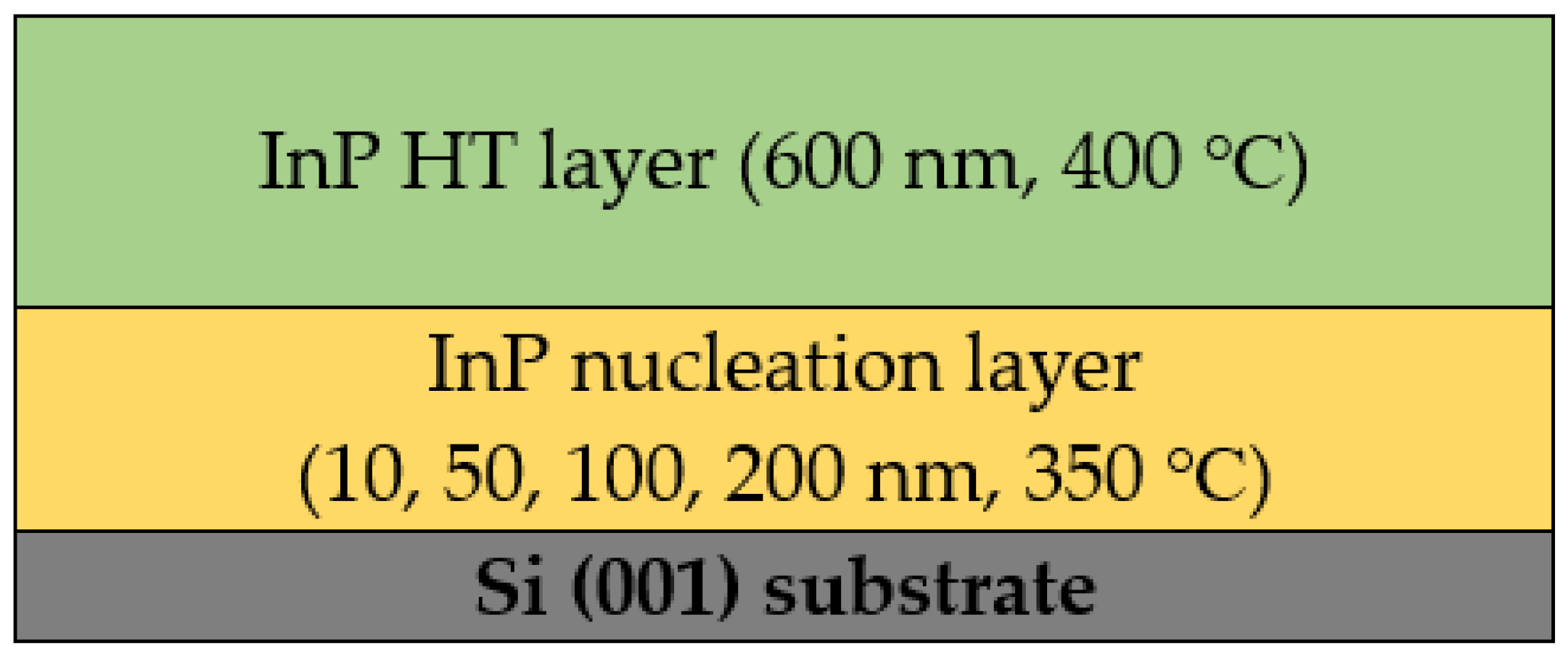
2. Experimental Section

All the samples in this study were grown on 2-inch (100)-oriented silicon substrates by using a VG Semicon V90H GSMBE system. The experimental processes are as follows: Initially, the Si(001) substrates were chemically cleaned for 30 s with buffered oxide etch (BOE) solution in which the ratio of HF and NH4F is 1:6, whose purpose is to remove the oxide layer before the epitaxial growth. Next, it was rinsed in de-ionized water and then dried with nitrogen, and then, the Si substrates were annealed in the MBE chamber at 625 ℃ for 30 mins to remove the surface residual oxide, which was monitored by a high energy electron diffraction (RHEED) system. After that, the temperature was reduced to 350 ℃ for the growth of the low-temperature nucleation layer, and the group V and III sources are Phosphorus (PH3) cracking cell and indium, respectively. Then, InP nucleation layers with different thicknesses were grown on Si(001) substrates whose thickness was controlled by the growth time: 1 min 9 s (10 nm), 5 min 47 s (50 nm),11 min 34 s (100 nm) and 21 min 9 s (200 nm). The growth time was calculated by the growth rate of InP, which is approximately 1.44 Å/s. After these steps, the substrate temperature was increased up to 400 ℃ at a rate of 0.5 ℃/s to growth high temperature (HT) InP layer with the thickness of 600 nm (69 min 26 s). Finally, in order to evaluate the effect of different nucleation layer thickness on the quality of heteroepitaxial layer, we used HR-XRD to investigate the crystal quality, used AFM to examine the microstructure of InP-Si surface, and adopted TEM to study the distribution of dislocations caused by large lattice mismatch. Figure 1 shows the schematic diagram of InP direct heterogeneous epitaxial growth on Si(001) substrates.

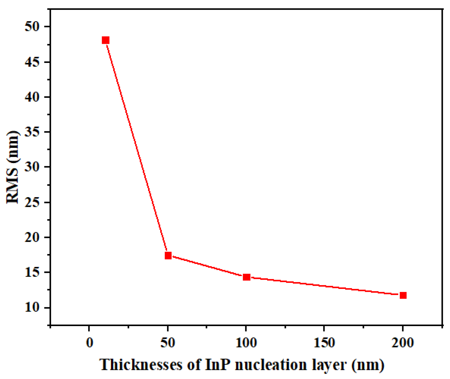
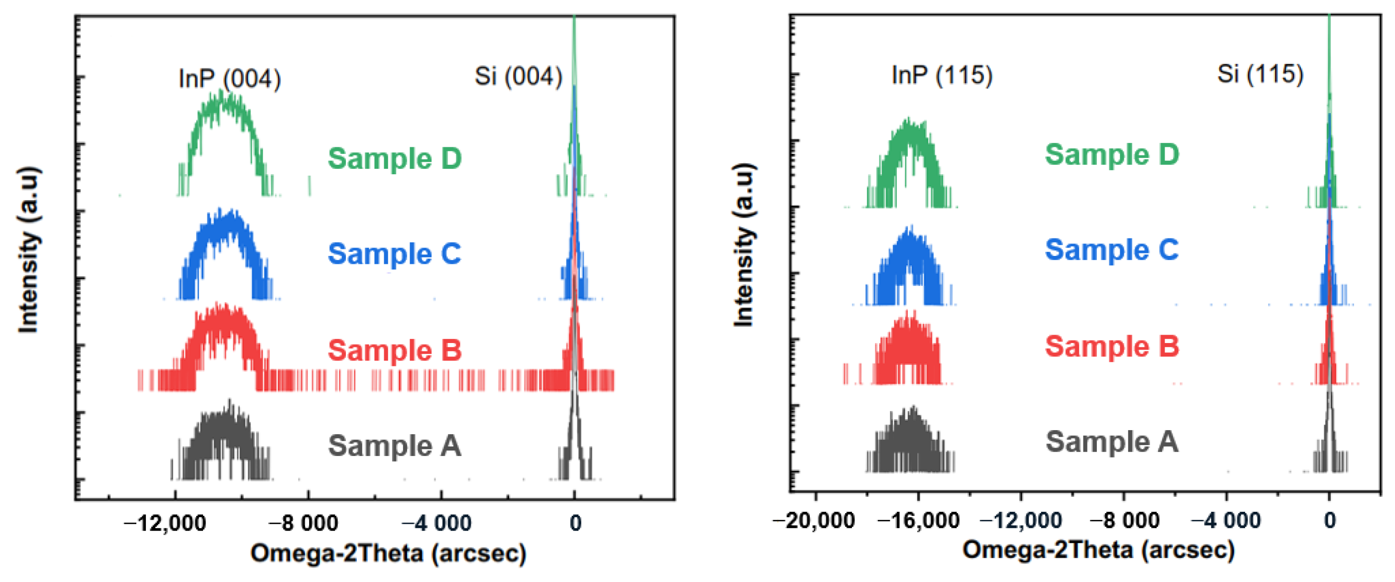
3. Results and Discussion

Figure 2 shows the surface morphology images of InP epilayers with different thicknesses of InP nucleation layer grown on Si substrates received from AFM in a 10 × 10 μm2 scanning area. The InP nucleation layer thickness of four samples was 10 nm, 50 nm, 100 nm, and 200 nm, corresponding to samples A, B, C, and D, respectively. The root-mean-square (RMS) values of the surface roughness are 48.2, 17.5, 14.4, and 11.8 nm for samples A, B, C, and D, respectively, which means that the thickness of the InP nucleation layer is a critical factor determining surface morphology. The RMS results measured by AFM are plotted as a function of the thickness of the InP nucleation layer, which is shown in Figure 3. It can be found that with the InP nucleation layer thicknesses increase, the surface roughness of epitaxial layers decreases, which reveals that the InP nucleation layer grown with 200 nm has the best crystalline quality compared with other samples.
TEM was used to investigate the microstructure of InP epilayers with 200 nm InP nucleation layer thickness. Because of the large lattice mismatch between the InP nucleation layer and Si substrate, it can be found that the InP nucleation layers tend to release the strain energy by an island growth: at the initial growth stage, the morphology of InP epilayers was changed from near-amorphous morphology to large islands with different sizes, and the phenomenon of island merging is obvious in Figure 4a. Meanwhile, many mismatched dislocations were generated in these islands during growth, which propagated to the surface of the material with the growth of the high-temperature InP layer, reducing the material quality of the crystal (Figure 4b).
The main reason for this phenomenon is that the migration power of the surface atoms is greatly reduced by the excessively low growth temperature, particularly for the indium atoms, which possess a bigger atomic radius and mass. Therefore, a too-thin thickness of the InP nucleation layer will cause an uneven distribution of atoms on the surface, resulting in a large number of island structures. However, as the thickness of the low-temperature nucleation layer increases, the island structure becomes larger and merges, decreasing the number of defects, and the surface morphology gradually becomes smooth. Therefore, the thicker the low-temperature nucleation layer is, the better the crystallization quality of the InP high-temperature layer will be. Moreover, after growing the low-temperature nucleation layer, it is usually annealed at a high temperature, which is similar to the principle of increasing the growth thickness. Both approaches can decrease the number of defects and make the surface smoother. Therefore, considering the growth time and cost, we believe that it is unnecessary to grow the nucleation layer too thick. After the growth of the nucleating layer, annealing at a high temperature for a period of time can not only improve the crystallization quality by achieving the same effect as increasing the growth thickness but also reduce the growth time and improve the experimental efficiency.
HR-XRD scan curves of different thicknesses of the InP nucleation layer on Si(001) are shown in Figure 5. It is observed that with the InP nucleation layer thickness increased from 10 nm to 200 nm, the peak intensity increased, and the FWHM values decreased, which indicates the crystal quality became better. Furthermore, according to the HR-XRD measurements, the extracted peak intensity and full width at half maximum (FWHM) of four samples are listed in Table 1, and the following formula can be used to describe the relationship between the FWHM and the thread dislocation density (TDD) [30].
N dis = ( FWHM ) 2 9 b 2
where Ndis is dislocation density, FWHM is in radians whose value is summarized in Table 1, b is Burgers vector of materials. Compared to the other samples, sample D with 200 nm InP nucleation layer shows the smallest FWHM and the minimum TDD value, which provides the best crystalline quality, indicating that the quality of the overall InP film has been significantly influenced by the thickness of the nucleation layer, and as the thickness of nucleation layer increases, the quality of epitaxial layer becomes better.

4. Conclusions

The InP epilayers with different nucleation layer thicknesses were grown on Si(001) substrates, which were fabricated by using the two-step growth technique. In our experiment, we find that a too thin nucleation layer will lead to an uneven distribution of atoms on the surface, resulting in a poor crystalline quality of the InP epitaxial layer and surface roughness of InP epilayer decreased by increasing the thickness of the InP nucleation layer. The best results are achieved with the nucleation layer thickness of 200 nm, which has the smoothest surface morphology, the biggest intensity, and the minimum FWHM of (004) and (115) Bragg peaks. Meanwhile, the results of the XRD and AFM analysis all illustrate that: the thicker the low-temperature nucleation layer is, the better the crystallization quality of the InP high-temperature layer will be.

Author Contributions

Conceptualization, S.Y. (Silu Yan); Methodology, S.Y. (Silu Yan); Validation, S.Y. (Silu Yan) and S.Y. (Shizheng Yang); Formal analysis, S.Y. (Silu Yan) and S.Y. (Shizheng Yang); Investigation, S.Y. (Silu Yan) and S.Y. (Shizheng Yang); Resources, H.L. and Y.Z.; Data curation, S.Y. (Silu Yan) and S.Y. (Shizheng Yang); Visualization, S.Y. (Silu Yan) and S.Y. (Shizheng Yang); Supervision, H.L. and Y.Z.; Project administration, H.L.; Funding acquisition, H.L. and Y.Z.; Writing—original draft, S.Y. (Silu Yan); Writing—review and editing, H.L. and S.Y. (Shizheng Yang). All authors have read and agreed to the published version of the manuscript.

Funding

This research was supported by the Key Research Development Program of Shaanxi (Program No. 2021GY-010) and the 111 Project of National 111 Center.

Institutional Review Board Statement

Not applicable.

Informed Consent Statement

Not applicable.

Data Availability Statement

All data included in this study are available upon request by contact with the corresponding author. The data are not publicly available due to no available online server in the research group temporarily.

Conflicts of Interest

The authors declare no conflict of interest.

References

  1. Hiraki, T.; Aihara, T.; Hasebe, K.; Fujiia, T.; Takedaa, K.; Nishia, H.; Kakitsukaa, T.; Fukudaa, H.; Tsuchizawaa, T.; Matsuoa, S. Heterogeneous Integration of III-V Semiconductors on Si Photonics Platform. ECS Trans. 2018, 86, 11–16. [Google Scholar] [CrossRef]
  2. Hancock, T.M.; Demmin, J.C. Heterogeneous and 3D Integration at DARPA. In Proceedings of the 2019 International 3D Systems Integration Conference (3DIC), Sendai, Japan, 8–10 October 2019; pp. 1–4. [Google Scholar]
  3. Dallesasse, J.M.; Carlson, J.A.; Ganjoo, M.; Espenhahn, L. Heterogeneous Integration for Silicon Photonic Systems: Challenges and Approaches. In Proceedings of the 2021 5th IEEE Electron Devices Technology & Manufacturing Conference (EDTM), Chengdu, China, 8–11 April 2021; pp. 1–3. [Google Scholar]
  4. Green, D.S.; Dohrman, C.L.; Demmin, J.; Zheng, Y.; Chang, T.H. A Revolution on the Horizon from DARPA: Heterogeneous Integration for Revolutionary Microwave/Millimeter-Wave Circuits at DARPA: Progress and Future Directions. IEEE Microw. Mag. 2017, 18, 44–59. [Google Scholar] [CrossRef]
  5. Park, J.S.; Tang, M.; Chen, S.; Liu, H. Heteroepitaxial Growth of III-V Semiconductors on Silicon. Crystals 2020, 10, 1163. [Google Scholar] [CrossRef]
  6. Kazior, T.E. Beyond CMOS: Heterogeneous integration of III-V devices, RF MEMS and other dissimilar materials/devices with Si CMOS to create intelligent microsystems. Philos. Trans. R. Soc. A-Math. Phys. Eng. Sci. 2014, 372, 20130105. [Google Scholar] [CrossRef] [Green Version]
  7. Weimann, N.G.; Johansen, T.K.; Stoppel, D.; Matalla, M.; Brahem, M.; Nosaeva, K.; Boppel, S.; Volkmer, N.; Ostermay, I.; Krozer, V.; et al. Transferred-Substrate InP/GaAsSb heterojunction bipolar transistor technology with fmax~0.53 THz. IEEE Trans. Electron Devices 2018, 65, 3704–3710. [Google Scholar] [CrossRef] [Green Version]
  8. Weimann, N. InP HBT technology for THz applications. In Proceedings of the 2020 IEEE International Symposium on Radio-Frequency Integration Technology (RFIT), Hiroshima, Japan, 2–4 September 2020; pp. 190–192. [Google Scholar]
  9. Hossain, M.; Shivan, T.; Hrobak, M.; Al-Sawaf, T.; Stoppel, D.; Yacoub, H.; Weimann, N.; Heinrich, W.; Krozer, V. A W-Band Transceiver Chip for Future 5G Communications in InP-DHBT Technology. In Proceedings of the 2020 15th European Microwave Integrated Circuits Conference (EuMIC), Utrecht, The Netherlands, 10–15 January 2021; pp. 193–196. [Google Scholar]
  10. Liu, W.K.; Lubyshev, D.; Fastenau, J.M.; Wu, Y.; Bulsara, M.T.; Fitzgerald, E.A.; Urteaga, M.; Ha, W.; Bergman, J.; Brar, B.; et al. Monolithic integration of InP-based transistors on Si substrates using MBE. J. Cryst. Growth 2009, 311, 1979–1983. [Google Scholar] [CrossRef]
  11. Kraemer, T.; Ostermay, I.; Jensen, T.; Johansen, T.K.; Schmueckle, F.; Thies, A.; Krozer, V.; Heinrich, W.; Krueger, O.; Traenkle, G.; et al. lnP-DHBT-on-BiCMOS Technology with fT/fmax of 400/3S0 GHz for heterogeneous integrated millimeter wave sources. IEEE Trans. Electron. Devices 2013, 60, 2209–2222. [Google Scholar] [CrossRef]
  12. Gutierrez-Aitken, A.; Chang-Chien, P.; Scott, D.; Hennig, K.; Kaneshiro, E.; Nam, P.; Cohen, N.; Ching, D.; Thai, K.; Oyama, B.; et al. Advanced Heterogeneous Integration of InP HBT and CMOS Si Technologies. In Proceedings of the 2010 IEEE Compound Semiconductor Integrated Circuit Symposium, Monterey, CA, USA, 3–6 October 2010. [Google Scholar]
  13. Li, Q.; Lau, K.M. Epitaxial growth of highly mismatched III-V materials on (001) silicon for electronics and optoelectronics. Prog. Cryst. Growth Charact. Mater. 2017, 63, 105–120. [Google Scholar] [CrossRef] [Green Version]
  14. Li, J.; Miao, G.; Zhang, Z.; Zeng, Y. Experiments and analysis of the two-step growth of InGaAs on GaAs substrate. Crystengcomm 2015, 17, 5808–5813. [Google Scholar] [CrossRef]
  15. Okumura, S.; Suzuki, R.; Tsunoda, K.; Nishino, H.; Sugiyama, M. Suppression of Three-Dimensional Pit Formation of InAs on GaSb (001) by Two-Step MBE. In Proceedings of the 2019 Compound Semiconductor Week (CSW), Nara, Japan, 19–23 May 2019. [Google Scholar]
  16. Nakamura, S.; Harada, Y.; Seno, M. Novel metalorganic chemical vapor deposition system for GaN growth. Appl. Phys. Lett. 1991, 58, 2021. [Google Scholar] [CrossRef]
  17. Nakamura, S. GaN growth using GaN buffer layer. Jpn. J. Appl. Phys. 1991, 30, L1705. [Google Scholar] [CrossRef]
  18. Waltereit, P.; Poblenz, C.; Rajan, S.; Wu, F.; Mishra, U.K.; Speck, J.S. Structural properties of GaN buffer layers on 4H-SiC (0001) grown by plasma-assisted molecular beam epitaxy for high electron mobility transistors. Jpn. J. Appl. Phys. 2004, 43, L1520. [Google Scholar] [CrossRef]
  19. Kim, Y.H.; Lee, J.Y.; Noh, Y.G.; Kim, M.D.; Kwon, Y.J.; Oh, J.E.; Gronsky, R. Effect of two-step growth on the heteroepitaxial growth of InSb thin film on Si (001) substrate: A transmission electron microscopy study. Appl. Phys. Lett. 2006, 89, 031919. [Google Scholar] [CrossRef]
  20. Cho, Y.-D.; Lee, I.-G.; Kim, S.-W.; Jun, D.-H.; Choi, I.-H.; Kwon, H.-M.; Shin, C.-S.; Park, K.-H.; Park, W.-K.; Kim, D.-H.; et al. Two-Step Growth of Epitaxial InP Layers by Metal Organic Chemical Vapor Deposition. J. Nanosci. Nanotechnol. 2016, 16, 5168–5172. [Google Scholar] [CrossRef] [PubMed]
  21. Shin, K.W.; Kim, H.; Kim, J.; Yang, C.; Lee, S.; Yoon, E. The effects of low temperature buffer layer on the growth of pure Ge on Si(001). Thin Solid Films 2010, 518, 6496–6499. [Google Scholar] [CrossRef]
  22. Barrett, C.S.C.; Martin, T.P.; Bao, X.Y.; Kennon, E.L.; Gutierrez, L.; Martin, P.; Sanchez, E.; Jones, K.S. Effect of bulk growth temperature on antiphase domain boundary annihilation rate in MOCVD-grown GaAs on Si(001). J. Cryst. Growth 2016, 450, 39–44. [Google Scholar] [CrossRef]
  23. Li, J.; Guo, Z.; Zhao, L.; Jia, Z.; Zhang, M.; Zhao, L. Effect of thicknesses of InP epilayers on InP/GaAs heterostructure. Surf. Interface Anal. 2018, 50, 27–31. [Google Scholar] [CrossRef]
  24. Kim, T.W.; Jung, M.; Park, T.H.; Cho, J.W.; Park, H.L. Structural and optical properties of InP/GaAs strained heterostructures grown by metal-organic chemical vapor deposition. Thin Solid Films. 1995, 257, 36–39. [Google Scholar] [CrossRef]
  25. Lee, S.; Cho, Y.J.; Park, J.; Shin, K.W.; Hwang, E.; Lee, S.; Lee, M.; Cho, S.; Su Shin, D.; Park, J.; et al. Effects of growth temperature on surface morphology of InP grown on patterned Si(001) substrates. J. Cryst. Growth 2015, 416, 113–117. [Google Scholar] [CrossRef]
  26. Kwoen, J.; Jang, B.; Lee, J.; Kageyama, T.; Watanabe, K.; Arakawa, Y. All MBE grown InAs/GaAs quantum dot lasers on on-axis Si (001). Opt. Express 2018, 26, 11568. [Google Scholar] [CrossRef]
  27. Liu, A.Y.; Peters, J.; Huang, X.; Jung, D.; Norman, J.; Lee, M.L.; Gossard, A.C.; Bowers, J.E. Electrically pumped continuous-wave 1.3 μm quantum-dot lasers epitaxially grown on on-axis (001) GaP/Si. Opt. Lett. 2017, 42, 338–341. [Google Scholar] [CrossRef] [PubMed]
  28. Jung, D.; Callahan, P.G.; Shin, B.; Mukherjee, K.; Gossard, A.C.; Bowers, J.E. Low threading dislocation density GaAs growth on on-axis GaP/Si (001). J. Appl. Phys. 2017, 122, 225703. [Google Scholar] [CrossRef] [Green Version]
  29. Yang, S.; Lv, H.; Ai, L.; Tian, F.; Yan, S.; Zhang, Y. Influence of Growth Temperature of the Nucleation Layer on the Growth of InP on Si (001). Coatings 2019, 9, 823. [Google Scholar] [CrossRef] [Green Version]
  30. Liu, X.; Song, H.; Miao, G.Q.; Jiang, H.; Cao, L.; Li, D.; Sun, X.; Chen, Y. Influence of thermal annealing duration of buffer layer on the crystalline quality of In 0.82 Ga 0.18 As grown on InP substrate by LP-MOCVD. Appl. Surf. Sci. 2011, 257, 1996. [Google Scholar] [CrossRef]
Figure 1. Schematic of InP epitaxial structures on Si(001) substrate.
Crystals 12 00462 g001
Figure 2. AFM images of the different thickness of InP epilayer grown at 350 °C: (A) 10 nm, (B) 50 nm, (C) 100 nm, and (D) 200 nm.
Crystals 12 00462 g002
Figure 3. Plot of the RMS roughness of InP films versus different thicknesses of InP nucleation layer.
Crystals 12 00462 g003
Figure 4. (a,b) Cross-sectional TEM images of the InP nucleation layers grown on Si(001).
Crystals 12 00462 g004
Figure 5. (004) and (115) omega-2theta HR-XRD scan curves for all Samples.
Crystals 12 00462 g005
Table 1. Intensity and FWHM of (004) and (115) Bragg peaks for all samples.
SampleIntensity of 004 (a.u)FWHM of 004 (arcsec)Intensity of 115 (a.u)FWHM of 115 (arcsec)
A751400.766821,619.11
B1381353.6861806.8
C1551178.281251639.5
D394901.442211464.3
Publisher’s Note: MDPI stays neutral with regard to jurisdictional claims in published maps and institutional affiliations.

