
ZnO Films from Thermal Oxidation of Zn Films: Effect of the Thickness of the Precursor Films on the Structural, Morphological, and Optical Properties of the Products

 ,
,
Abstract
:1. Introduction
2. Materials and Methods
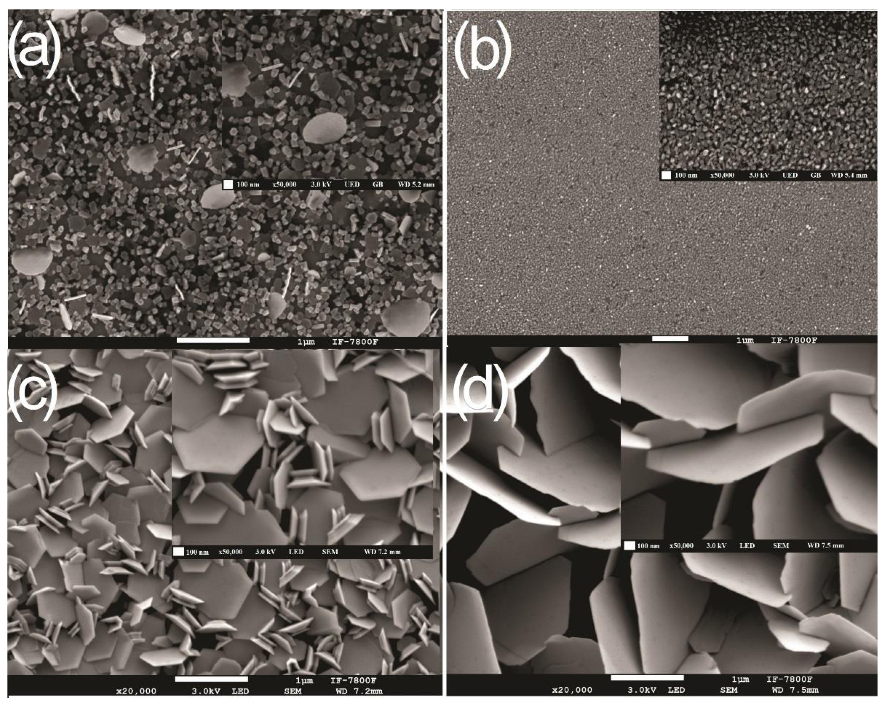
3. Results and Discussion
4. Conclusions
Author Contributions
Funding
Institutional Review Board Statement
Informed Consent Statement
Data Availability Statement
Acknowledgments
Conflicts of Interest
Appendix A
References
- Kazmierczak-Balata, A.; Grzadziel, L.; Guziewicz, M.; Venkatachalapathy, V.; Kutznetsov, A.; Krzywiecki, M. Correlations of thermal properties with grain structure, morphology, and defect balance in nanoscale polycrystalline ZnO films. Appl. Surf. Sci. 2021, 546, 149095. [Google Scholar] [CrossRef]
- Samavati, A.; Awang, A.; Samavati, Z.; Ismail, A.F.; Othman, M.H.D.; Velashjerdi, M.; Eisaabadi, B.G.; Rostami, A. Influence of ZnO nanostructure configuration on tailoring the optical bandgap: Theory and experiment. Mater. Sci. Eng. B 2021, 263, 114811. [Google Scholar] [CrossRef]
- Okada, T.; Tateyama, C.; Hoshino, K.; Kawashima, T.; Washio, K. Aluminum and vanadium co-doping effects on the optical and electrical properties of oriented ZnO films. Mater. Res. Exp. 2021, 8, 016402. [Google Scholar] [CrossRef]
- Hoffmann, R.C.; Sanctis, S.; Liedke, M.O.; Butterling, M.; Wagner, A.; Njel, C.; Schneider, J.J. Zinc Oxide Defect Microstructure and Surface Chemistry Derived from Oxidation of Metallic Zinc: Thin-Film Transistor and Sensor Behavior of ZnO Films and Rods. Chem. Eur. J. 2021, 27, 5422–5431. [Google Scholar] [CrossRef]
- Johar, M.A.; Afzal, R.A.; Alazba, A.A.; Manzoor, U. Photocatalysis and Bandgap Engineering Using ZnO Nanocomposites. Adv. Mater. Sci. Eng. 2015, 2015, 934587. [Google Scholar] [CrossRef] [Green Version]
- Khanlary, M.R.; Vahedi, V.; Reyhani, A. Synthesis and Characterization of ZnO Nanowires by Thermal Oxidation of Zn Thin Films at Various Temperatures. Molecules 2012, 17, 5021–5029. [Google Scholar] [CrossRef] [Green Version]
- Kajikawa, Y. Texture development of non-epitaxial polycrystalline ZnO films. J. Cryst. Growth 2006, 289, 387–394. [Google Scholar] [CrossRef]
- Czyzowska, A.; Barbasz, A. A review: Zinc oxide nanoparticles –friends or enemies? Int. J. Environ. Health Res. 2020, 2020, 1805415. [Google Scholar] [CrossRef]
- Perez Espitia, P.J.; Ferreira Soares, N.F.; dos Reis Coimbra, J.S.; de Andrade, N.J.; Souza Cruz, R.; Alves Medeiros, E.A. Zinc oxide nanoparticles: Synthesis, antimicrobial activity and food packaging applications. Food Bioprocess Technol. 2012, 5, 1447–1464. [Google Scholar] [CrossRef]
- Singh, T.A.; Sharma, A.; Tejwan, N.; Ghosh, N.; Das, J.; Sil, P.C. A state of the art review on the synthesis, antibacterial, antioxidant, antidiabetic and tissue regeneration activities of zinc oxide nanoparticles. Adv. Colloid Interface Sci. 2021, 295, 102495. [Google Scholar] [CrossRef]
- Jin, S.-E.; Jin, H.-E. Antimicrobial Activity of Zinc Oxide Nano/Microparticles and Their Combinations against Pathogenic Microorganisms for Biomedical Applications: From Physicochemical Characteristics to Pharmacological Aspects. Nanomaterials 2021, 11, 263. [Google Scholar] [CrossRef] [PubMed]
- Mishra, P.K.; Mishra, H.; Ekielski, A.; Talegaonkar, S.; Vaidya, B. Zinc oxide nanoparticles: A promising nanomaterial for biomedical applications. Drug Discov. Today 2017, 22, 1825–1834. [Google Scholar] [CrossRef] [PubMed]
- Wang, Z.L. Nanostructures of zinc oxide. Mater. Today 2004, 7, 26–33. [Google Scholar] [CrossRef]
- Joraid, A.A.; Soleiman, A.S.; Al-Maghrabi, M.A.; Almutairy, M.H. Studies of crystallization kinetics and optical properties of ZnO films prepared by sol-gel technique. J. Sol-Gel Sci. Technol. 2021, 97, 523–539. [Google Scholar] [CrossRef]
- Ul Haq, A.N.; Nadhman, A.; Ullah, I.; Mustafa, G.; Yasinzai, M.; Khan, I.J. Synthesis Approaches of Zinc Oxide Nanoparticles: The Dilemma of Ecotoxicity. J. Nanomater. 2017, 2017, 8510342. [Google Scholar] [CrossRef]
- Kolodziejczak-Radzimska, A.; Jesionowski, T. Zinc Oxide—From Synthesis to Application: A Review. Materials 2014, 7, 2833–2881. [Google Scholar] [CrossRef] [Green Version]
- Balela, M.D.L.; Pelicano, C.M.O.; Ty, J.D.; Yanagi, H. Formation of zinc oxide nanostructures by wet oxidation of vacuum deposited Zn thin film. Opt. Quant. Electron. 2017, 49, 3. [Google Scholar] [CrossRef]
- Acuña-Avila, P.E.; López, R.; Vigueras-Santiago, E.; Hernández-López, S.; Camacho-López, M.; Ornelas-Gutierrez, C.; Antunez, W. Effect of thermal treatment on Zn nanodisks. AIP Adv. 2015, 5, 067109. [Google Scholar] [CrossRef] [Green Version]
- Singh, S.; Chakrabarti, P. Optical Chracterization of ZnO Thin Films Grown by Thermal Oxidation of Metallic Zinc. Adv. Sci. Eng. Med. 2013, 5, 677–682. [Google Scholar] [CrossRef]
- Zhang, D.; Wang, C.; Liu, Y.; Shi, Q.; Wang, W. High c-axis preferred orientation ZnO thin films prepared by oxidation of metallic zinc. Opt. Laser Technol. 2012, 44, 1136–1140. [Google Scholar] [CrossRef]
- Dhananjay; Nagaraju, J.; Krupanidhi, S.B. Investigations on zinc oxide thin films grown on Si (1 0 0) by thermal oxidation. Mater. Sci. Eng. B 2007, 137, 126–130. [Google Scholar] [CrossRef]
- Rusu, G.G.; Girtan, M.; Rusu, M. Preparation and characterization of ZnO thin films prepared by thermal oxidation of evaporated Zn thin films. Superlattices Microstruct. 2007, 42, 116–122. [Google Scholar] [CrossRef]
- Li, Z.W.; Gao, W.; Reeves, R.J. Zinc oxide films by thermal oxidation of zinc thin films. Surf. Coat. Technol. 2005, 198, 319–323. [Google Scholar] [CrossRef]
- Zhao, J.; Hu, L.; Wang, Z.; Zhao, Y.; Liang, X.; Wang, M. High-quality ZnO films prepared by low temperature oxidation of metallic zinc. Appl. Surf. Sci. 2004, 229, 311–315. [Google Scholar] [CrossRef]
- Wang, Y.G.; Lau, S.P.; Lee, H.W.; Yu, S.F.; Tay, B.K.; Zhang, X.H.; Hng, H.H. Photoluminiscence study of ZnO films prepared by thermal oxidation of Zn metallic films in air. J. Appl. Phys. 2003, 94, 354–358. [Google Scholar] [CrossRef]
- Cho, S.; Ma, J.; Kim, Y.; Sun, Y.; Wong, G.K.L.; Ketterson, J.B. Photoluminiscence and ultraviolet lasing of polycrystalline ZnO thin films prepared by the oxidation of the metallic Zn. Appl. Phys. Lett. 1999, 75, 2761–2763. [Google Scholar] [CrossRef]
- Fanni, L.; Abersold, B.A.; Alexander, D.T.L.; Ding, L.; Morales Masis, M.; Nicolay, S.; Ballif, C. c-texture versus a-texture low pressure metalorganic chemical vapor deposition ZnO films: Lower resistivity despite smaller grain size. Thin Solid Film. 2014, 565, 1–6. [Google Scholar] [CrossRef]
- Lin, S.-S.; Huang, J.-L. Effect of thickness on the structural and optical properties of ZnO films by r.f. magnetron sputtering. Surf. Coat. Technol. 2004, 185, 222–227. [Google Scholar] [CrossRef] [Green Version]
- Morkoc, H.; Özgür, Ü. Zinc Oxide: Fundamentals, Materials and Device Technology; John Wiley and Sons: Danves, MA, USA, 2009. [Google Scholar]
- Fujimura, N.; Nishihara, T.; Goto, S.; Xu, J.; Ito, T. Control of preferred orientation for ZnOx films: Control of self-texture. J. Cryst. Growth 1993, 130, 269–279. [Google Scholar] [CrossRef]
- Goto, S.; Fujimura, N.; Nishihara, T.; Ito, T. Heteroepitaxy of zinc oxide films, considering non-epitaxial preferential orientation. J. Cryst. Growth 1991, 115, 816–820. [Google Scholar] [CrossRef]
- Mekhnache, M.; Drici, A.; Hamideche, L.S.; Benzarouk, H.; Amara, A.; Cattin, L.; Bernede, J.C.; Guerioune, M. Properties of ZnO thin films deposited on (glass, ITO and ZnO:Al) substrates. Superlattices Microstruct. 2011, 49, 510–518. [Google Scholar] [CrossRef]
- Prepelita, P.; Medianu, R.; Sbarcea, B.; Garoi, F.; Filipescu, M. The influence of using different substrates on the structural and optical characteristics of ZnO thin films. Appl. Surf. Sci. 2010, 256, 1807–1811. [Google Scholar] [CrossRef]
- Triboulet, R.; Perriere, J. Epitaxial growth of ZnO films. Prog. Cryst. Growth Charact. Mater. 2003, 47, 65–138. [Google Scholar] [CrossRef]
- Moutinho, H.R.; Hasoon, F.S.; Abulfotuh, F.; Kazmerski, L.L. Investigation of polycrystalline CdTe thin films deposited by physical vapor deposition, close spaced sublimation, and sputtering. J. Vac. Sci. Technol. A 1995, 13, 2877–2883. [Google Scholar] [CrossRef]
- Harris, G.B. X. Quantitative measurement of preferred orientation in rolled uranium bars. Lond. Edinb. Dublin Philos. Mag. J. Sci. 1952, 43, 113–123. [Google Scholar] [CrossRef]
- Percharsky, V.K.; Zavalij, P.Y. Fundamentals of Powder Diffraction and Structural Characterization of Materials, 2nd ed.; Springer: New York, NY, USA, 2009. [Google Scholar] [CrossRef]
- Klug, H.P.; Alexander, L.E. X-Ray Diffraction Procedures: For Polycrystalline and Amorphous Materials, 2nd ed.; John Wiley and Sons: Danves, MA, USA, 1974; ISBN 978-0-471-49369-3. [Google Scholar]
- Solís-Palomar, F.; Martínez, E.; Meléndrez, M.F.; Pérez-Tijerina, E. Growth of vertically aligned ZnO nanorods using textured ZnO films. Nanoscale Res. Lett. 2011, 6, 524. [Google Scholar] [CrossRef] [PubMed] [Green Version]
- Lee, H.S.; Lee, J.Y.; Kim, T.W.; Kim, D.W.; Cho, W.J. Formation mechanism of preferential c-axis oriented ZnO thin films grown on pi-Si substrates. J. Mater. Sci. 2004, 39, 3525–3528. [Google Scholar] [CrossRef]
- Deng, H.; Russell, J.J.; Lamb, R.M.; Jiang, B.; Li, Y.; Zhou, X.Y. Microstructure control of ZnO thin films prepared by single source chemical vapor deposition. Thin Solid Film. 2004, 458, 43–46. [Google Scholar] [CrossRef]
- Choi, J.H.; Tabata, H.; Kawai, T. Initial preferred growth in zinc oxide thin films on Si and amorphous substrates by a pulsed laser deposition. J. Cryst. Growth 2001, 226, 493–500. [Google Scholar] [CrossRef]
- Devan, R.S.; Lin, J.-H.; Huang, Y.-J.; Yang, C.-C.; Wun, S.Y.; Liou, Y.; Ma, Y.-R. Two-dimensional single-crystalline Zn hexagonal nanoplates: Size-controllable synthesis and X-ray diffraction study. Nanoscale 2011, 3, 4339–4345. [Google Scholar] [CrossRef]
- Jaber, B.; Laanab, L. One step synthesis of ZnO nanoparticles in free organic medium: Structural and optical characterizations. Mater. Sci. Semicond. Process. 2014, 27, 446–451. [Google Scholar] [CrossRef]
- Wiersma, D.S. The physics and applications of random lasers. Nat. Phys. 2008, 4, 359–367. [Google Scholar] [CrossRef]
- Torres-Torres, C.; Trejo-Valdez, M.; Sobral, H.; Santiago-Jacinto, P.; Reyes-Esqueda, J.A. Stimulated Emission and Optical Third-Order Nonlinearity in Li-Doped ZnO Nanorods. J. Phys. Chem. C 2009, 113, 13515–13521. [Google Scholar] [CrossRef]
- Luan, F.; Gu, B.; Gomez, A.S.L.; Yong, K.-T.; Wen, S.; Prasad, P.N. Lasing in nanocomposite random media. Nano Today 2015, 10, 168–192. [Google Scholar] [CrossRef]
- Yu, S.F.; Yuen, C.; Lau, S.P.; Lee, H.W. Zinc oxide thin-film random lasers on silicon substrate. Appl. Phys. Lett. 2004, 84, 3244–3246. [Google Scholar] [CrossRef]
- Fallert, J.; Dietz, R.J.B.; Hauser, M.; Stelzl, F.; Klingshirn, C.; Kalt, H. Random lasing in ZnO nanocrystals. J. Lumin. 2009, 129, 1685–1688. [Google Scholar] [CrossRef]
- Nakamura, T.; Firdaus, K.; Adachi, S. Electron-hole plasma lasing in a ZnO random laser. Phys. Rev. B 2012, 86, 205103. [Google Scholar] [CrossRef]
- John, S. Localization of Light. Phys. Today 1991, 44, 32–40. [Google Scholar] [CrossRef]
- Andreasen, J.; Asatryan, A.A.; Botten, L.C.; Byrne, M.A.; Cao, H.; Ge, L.; Labonté, L.; Sebbah, P.; Stone, A.D.; Türeci, H.E.; et al. Modes of random lasers. Adv. Opt. Photon. 2011, 3, 88–127. [Google Scholar] [CrossRef]
- Segev, M.; Silberberg, Y.; Christodoulides, D.N. Anderson localization of light. Nat. Photon 2013, 7, 197–204. [Google Scholar] [CrossRef]
- Meulenkamp, E.A. Synthesis and Growth of ZnO Nanoparticles. J. Phys. Chem. B 1998, 102, 5566–5572. [Google Scholar] [CrossRef]
- Meulenkamp, E.A. Size Dependence of the Dissolution of ZnO Nanoparticles. J. Phys. Chem. B 1998, 102, 7764–7769. [Google Scholar] [CrossRef]
- McCluskey, M.D.; Jokela, S.J. Defects in ZnO. J. Appl. Phys. 2009, 106, 071101. [Google Scholar] [CrossRef] [Green Version]
- Janotti, A.; Van de Walle, C.G. Oxygen vacancies in ZnO. Appl. Phys. Lett. 2005, 87, 122102. [Google Scholar] [CrossRef]
- Srikant, V.; Clarke, D.R. On the optical band gap of zinc oxide. J. App. Phys. 1998, 83, 5447–5451. [Google Scholar] [CrossRef]


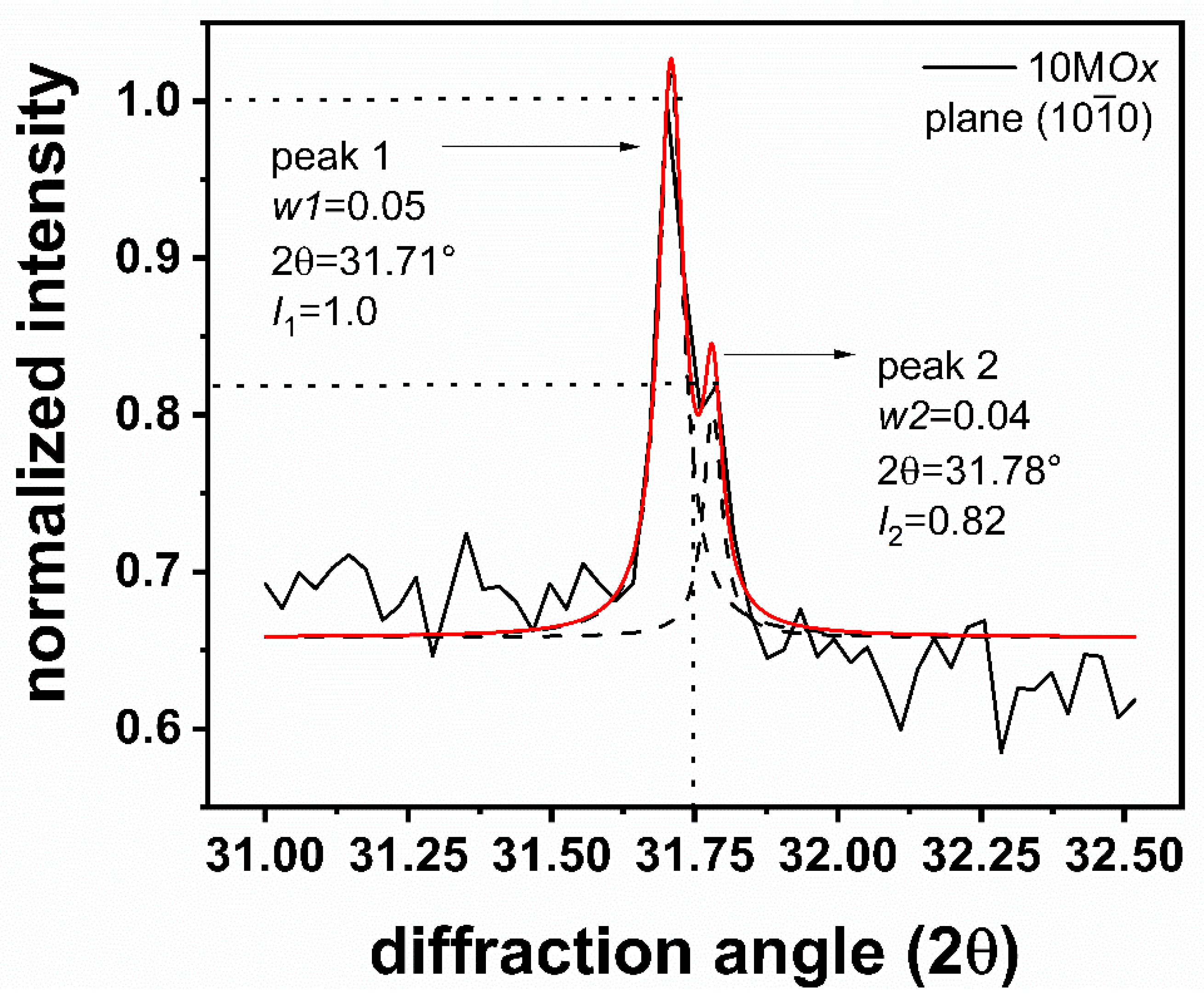
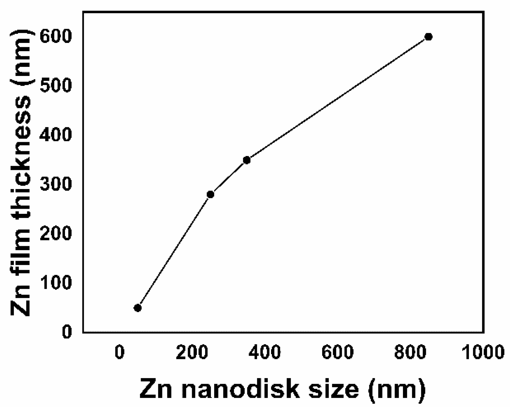
| Sample | Zn Film Thickness (nm) | ZnO Film Thickness (nm) | TC (abcd) | D (nm) |
|---|---|---|---|---|
| A1Ox | 50 | 50 | (0001):2.0 | 27 |
| 3MOx | 280 | 420 | (100):1.6 | 68 |
| 6MOx | 350 | 480 | (100):1.5 | 58 |
| 10MOx | 600 | 610 | (100):3.0 | 413 |
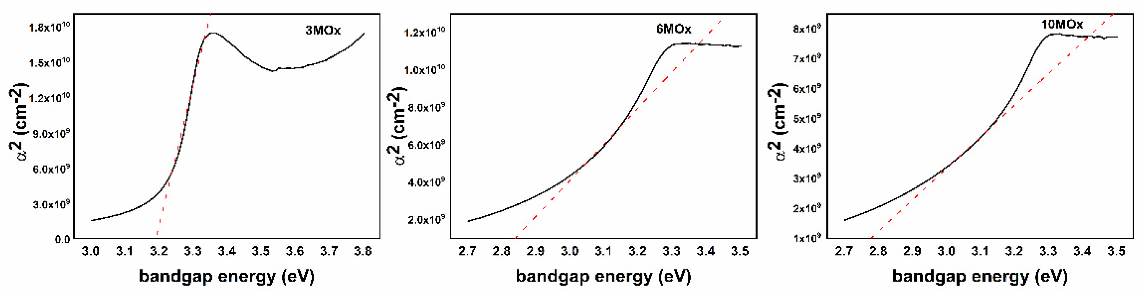
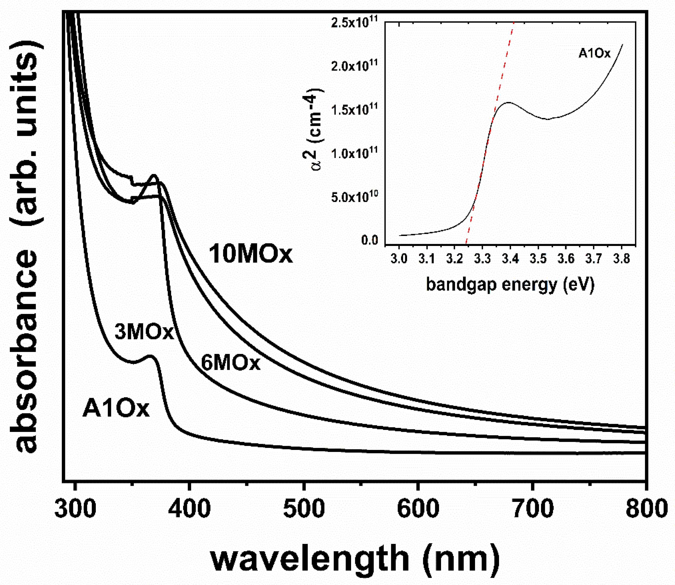
| Sample | Tauc Plot Method (eV) | λ1/2 Method (eV) |
|---|---|---|
| A1Ox | 3.24 | 3.26 |
| 3MOx | 3.18 | 3.21 |
| 6MOx | 2.84 | 2.85 |
| 10MOx | 2.78 | 2.78 |
Publisher’s Note: MDPI stays neutral with regard to jurisdictional claims in published maps and institutional affiliations. |
© 2022 by the authors. Licensee MDPI, Basel, Switzerland. This article is an open access article distributed under the terms and conditions of the Creative Commons Attribution (CC BY) license (https://creativecommons.org/licenses/by/4.0/).
Share and Cite
Sánchez-Dena, O.; Hernández-López, S.; Camacho-López, M.A.; Acuña-Ávila, P.E.; Reyes-Esqueda, J.A.; Vigueras-Santiago, E. ZnO Films from Thermal Oxidation of Zn Films: Effect of the Thickness of the Precursor Films on the Structural, Morphological, and Optical Properties of the Products. Crystals 2022, 12, 528. https://doi.org/10.3390/cryst12040528
Sánchez-Dena O, Hernández-López S, Camacho-López MA, Acuña-Ávila PE, Reyes-Esqueda JA, Vigueras-Santiago E. ZnO Films from Thermal Oxidation of Zn Films: Effect of the Thickness of the Precursor Films on the Structural, Morphological, and Optical Properties of the Products. Crystals. 2022; 12(4):528. https://doi.org/10.3390/cryst12040528
Chicago/Turabian StyleSánchez-Dena, Oswaldo, Susana Hernández-López, Marco Antonio Camacho-López, Pedro Estanislao Acuña-Ávila, Jorge Alejandro Reyes-Esqueda, and Enrique Vigueras-Santiago. 2022. "ZnO Films from Thermal Oxidation of Zn Films: Effect of the Thickness of the Precursor Films on the Structural, Morphological, and Optical Properties of the Products" Crystals 12, no. 4: 528. https://doi.org/10.3390/cryst12040528