Abstract
The results of an experimental study of the abnormal domain structure kinetics in lithium niobate single crystals with a surface layer modified by soft proton exchange are presented. Domain switching in a wide field range allowed two qualitatively different types of domain structure evolution to be revealed: (1) the traditional growth of hexagonal domains in fields higher than 21.5 kV/mm and (2) the abnormal growth of stripe domains oriented along the Y crystallographic directions in the field range from 3.8 to 21.5 kV/mm. The stripe domains had a width up to 4 µm and depth up to 30 µm. It was shown that the time dependence of the total length of stripe domains could be analyzed in terms of the modified Kolmogorov–Avrami approach, taking into account the transition from the one-dimensional β-model to the one-dimensional α-model. The possibility of the controllable creation of a quasi-periodic structure of stripe domains with an average period of 5 µm by a two-stage polarization switching process was demonstrated. The formation and growth of stripe domains were considered in terms of the kinetic approach to the evolution of the domain structure as a result of the domain walls’ motion under inefficient screening conditions caused by the presence of a modified surface layer. The abnormally low threshold fields were attributed to a presence of a “built-in” field facilitating switching, created by a composition gradient induced by soft proton exchange.
1. Introduction
Crystals of uniaxial ferroelectric lithium niobate (LiNbO3, LN) are used in nonlinear and integral optics due to the large values of optical, electro-optical, and acousto-optic coefficients. The formation of periodical domain structures (PDS) in LN makes it possible to realize the quasi-phasematching conditions for nonlinear optical transformations, such as second harmonic generation and parametric light generation with record efficiency [1,2,3,4]. The creation of integrated optics devices based on LN requires the formation of PDS in optical waveguides [5,6]. Proton exchange (PE) is a widely used technique for creating optical waveguides by replacing Li+ ions with H+ protons [7], which utilize benzoic acid as a proton source. This process leads to an increase in the refractive index for an extraordinary wave and to a decrease in it for an ordinary wave in LN [8]. Changing the composition of the proton source makes it possible to obtain different dependencies of the refractive index on the depth: (a) a “step profile” with “hard” proton exchange in pure benzoic acid [7] and a “gradient profile” with “soft” proton exchange in benzoic acid with the addition of more than 2.7% lithium benzoate (soft proton exchange, SPE) [9,10]. It should be noted that among the considered PE methods only SPE conserves the ferroelectric properties in the waveguide [11].
It was previously shown that the evolution of the domain structure in PE LN depended significantly on the used PE procedure [12]. For hard PE, an increase in the thickness of the modified layer led to an increase in the threshold field, as well as to the formation of isolated nanodomains in front of the moving domain wall, thus forming a “broad domain boundary” [13]. For SPE, an abnormal decrease in the threshold field was observed, as well as the formation and growth of stripe domains. It has been noted that the discovered features of the domain kinetics in SPE LN are of considerable interest for the development of domain engineering; however, no systematic study of the domain structure evolution and geometric parameters of stripe domains in SPE LN has been carried out.
This paper presents the results of an experimental study of the abnormal kinetics of the domain structure in congruent LN single crystals with a surface layer modified by SPE (SPE CLN) in a wide field range. It is shown that the growth of stripe domains is observed up to the coercive (threshold) field in CLN. The possibility of the controllable formation of parallel quasi-regular structures of stripe domains from a “flat” domain wall by a change in the switching mode is demonstrated. The obtained results are explained in terms of the kinetic approach.
2. Materials and Methods
The studied samples represented 0.5 mm thick CLN plates cut perpendicular to the polar axis and polished to optical quality (Gooch & Housego, USA). The surface of the plates was modified by SPE at INPHINI, Nice, France. Annealing was carried out in benzoic acid with 3.0% lithium benzoate at 300 °C for 48 h.
The depth dependence of the concentration of H+ (C(h)) in the sample was measured by confocal Raman microscopy (CRM) with submicron spatial resolution using a confocal Raman microscope Alpha 300 AR (WITec, Germany) with excitation laser on wavelength 488 nm. The measured maximum intensity of the Raman spectrum line 3492 cm−1 corresponding to the oscillations of the OH group was proportional to the concentration of H+ ions [14] (Figure 1a,b). Based on the experimentally measured dependence C(h), the depth of the modified layer in our samples was about 2 microns (Figure 1c).
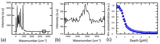
Figure 1.
(a) Raman spectrum of SPE CLN. (b) Spectral region with the 3492 cm−1 line. (c) Depth dependence of the amplitude of the 3492 cm−1 line (relative concentration of H+ ions) near the Z+ polar surface.
For domain switching, the sample was placed in a cell (Figure 2). Transparent electrodes based on saturated LiCl aqueous solution were used. Switching was carried out in the field range from 1 to 25 kV/mm by applying a single rectangular or triangular pulse with a duration from 100 ms to 300 s. The pulses were generated by an ADC/DAC board PCI-6251 (National Instruments, Austin, TX, USA) and amplified using a Trek 20/20c high-voltage amplifier (Trek Inc., Lockport, NY, USA) (Figure 2). The domain structure was in situ imaged using an LMA10 optical microscope (Carl Zeiss, Oberkochen, Germany) with a FASTCAM Mini UX100 high-speed video camera (Tech Imaging, Saugus, MA, USA) with a recording rate of up to 2500 frames/s.
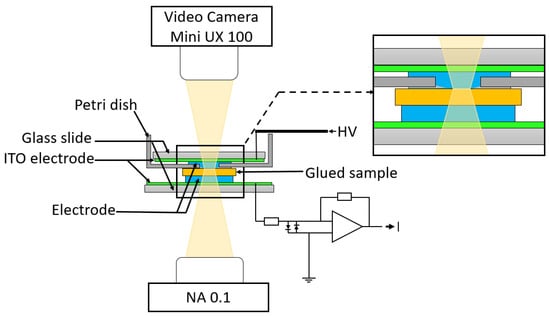
Figure 2.
Scheme of the setup for domain switching with in situ optical domain imaging.
The imaging of the static domain structure on the surface and in the bulk was carried out by the CRM based on the measurement of the spatial distribution of the shifts of the 581 cm−1 E(TO8) and 872 cm−1 A1(LO4) lines in the Raman spectrum during 2D scanning [15]. The spatial resolution of the method was about 500 nm.
3. Results
Switching of polarization in a wide range of fields allowed two qualitatively different types of domain structure evolution to be revealed: (1) the growth of oriented stripe domains in the field range from 3.8 to 21.5 kV/mm and (2) the growth of hexagonal domains for fields above 21.5 kV/mm.
The first type of domain structure evolution represents the formation of stripe domains and their growth in three Y crystallographic directions (Figure 3). The domain growth terminated when the domain encountered another stripe domain. The similar oriented growth of stripe domains was observed during the formation of a domain structure as a result of pulsed heating by IR laser radiation [16].
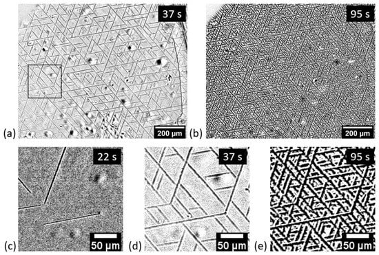
Figure 3.
Instantaneous optical images of the domain structure during polarization switching in increasing field. (a,b) At the time interval from the start of field pulse application: (a) 37 s (E = 8 kV/mm), (b) 95 s (E = 19 kV/mm). (c–e) Magnified fragment of the images marked in (a), at the time interval: (c) 22 s (E = 4.5 kV/mm), (d) 37 s (E = 8 kV/mm), (e) 95 s (E = 19 kV/mm). The field growth rate is 0.2 kV/(mm s).
Imaging of the domain structure after partial polarization reversal under the field of 5 kV/mm by the CRM method has shown that the stripe domains have a width of about 4 µm and a depth up to 30 µm (Figure 4).
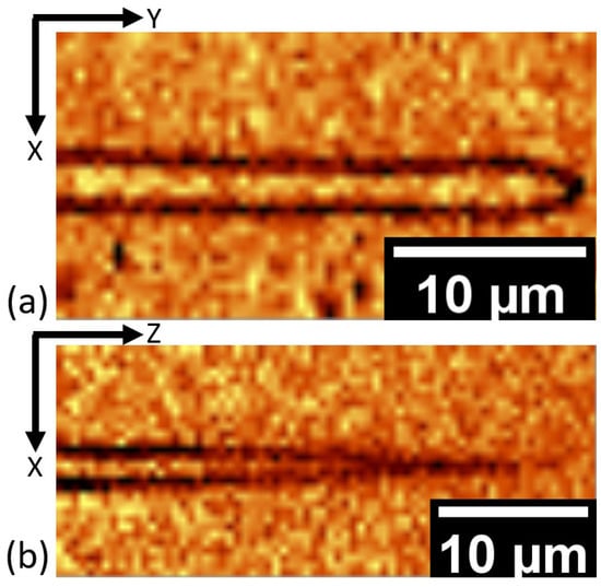
Figure 4.
CRM images of the stripe domains after partial polarization reversal: (a) view on the polar surface, (b) view at the XZ section.
To analyze the orientation distribution of the stripe domains, the results of in situ optical imaging of the domain structure evolution were processed by the following algorithm (Figure 5):
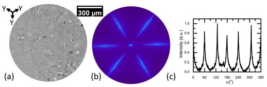
Figure 5.
(a) Instantaneous optical image of the domain structure after background subtraction. (b) The Fourier transform of the image. (c) The angular convolution of the Fourier transform. Applied field 8 kV/mm.
The algorithm for processing video recording frames and presenting the results was implemented using the OpenCV, SciPy, Skimage, and Matplotlib libraries [18,19,20,21].
The analysis demonstrated that the stripe domains are oriented along three equivalent directions, coinciding with the Y crystallographic directions in LN with C3v symmetry.
For switching in an increasing field, the time dependence of the total length of the stripe domains L (Figure 6a) and the average effective period of the structure T = A/L were analyzed, where A is the area of the analyzed region (Figure 6b).
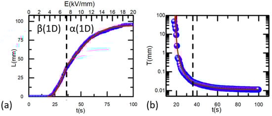
Figure 6.
Time dependencies of the domain structure parameters during switching in increasing field: (a) the total length of the stripe domains and (b) the effective period of the domain structure, fitted by Equation (7) and Equation (8), respectively.
The modified Kolmogorov–Avrami approach was used for the analysis of L(t) dependence [22,23,24]. Such an approach was previously used to analyze the time dependence of the total area of switched domains in ferroelectrics [25]. It was taken into account that, at the initial stage, the increase in L occurred due to the growth of stripe domains that appeared in lower fields on surface defects, which corresponds to the Kolmogorov–Avrami β-model. After that, the formation of new stripe domains and their subsequent growth prevail, which corresponds to the Kolmogorov–Avrami α-model (Figure 3). The general equation of L(t) dependence within a Kolmogorov–Avrami approach can be written as follows:
where Lmax is the maximum total length of stripe domains, α is the probability of nucleation per unit area, l(ξ,t) is the length of the stripe domain, which was formed at time ξ, by time t. For α-model α(t) = const; for β-model α(t) = δ(t).
It was assumed that the growth rate of the stripe domain was proportional to the field excess over the threshold value [26]:
where µ is the domain wall mobility and Eth is the threshold field. It is necessary to pay attention to the fact that the used formula is dissimilar to the Rayleigh law, which is used for the vibration of the domain walls as a whole [27].
In this case, it should be taken into account that the external field increases linearly with time:
where R = dE/dt is the field growth rate.
The length of one particular stripe domain l(ξ,t) can be found as follows:
Substituting Equations (2)–(4) into (1) and integrating, we obtain the following formula for the α-model:
where a = αµ, and tst = Eth/R is the start time of the switching process.
Similarly, for the β-model:
where b = µβR/2.
The measured time dependence of the total length of stripe domains (Lexp(t)) was fitted by the following formula:
where Δt is a time constant taking into account that the α-process starts when some part of the total length has been switched by the β-process.
Similarly, the time dependence of the average effective period of the domain structure was fitted by the formula:
The parameters Lmax = 96 mm, R = 0.2 kV/(mm·s), and Eth = 3.8 kV/mm were fixed during fitting. The values of the best fit parameters are as follows: a = (7.1 ± 0.5)·10−5 mm/(kV·s2), Δt = −(30 ± 1) s, and b = (1.8 ± 0.1)·10−3 s−2.
The growth of hexagonal domains was observed in the fields above 21.5 kV/mm, which corresponds to the threshold field for polarization reversal in CLN crystals [28]. In this case, the domain walls are parallel to the Y crystallographic directions (Figure 7).
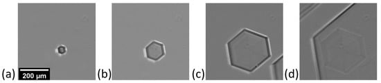
Figure 7.
Growth of hexagonal domains in the fields above 21.5 kV/mm. Instantaneous optical images of the domain structure during polarization reversal under the field of 22 kV/mm. The time intervals from the start of field pulse application: (a) 220 ms, (b) 228 ms, (c) 236 ms, (d) 244 ms. Optical microscopy, transmitted light.
The domain appeared after the merging of two hexagonal domains rapidly restored its hexagonal shape due to the formation and growth of ultrafast short-living walls (shape stability effect) (Figure 4) [29]. Thus, for partial polarization reversal, it is possible to obtain the flat strictly oriented domain walls of millimeter length, which can be used for the growth of stripe domains in fields less than 21.5 kV/mm.
Creation of Quasi-Periodic Domain Structures
The process of the formation of the quasi-periodic structure of stripe domains after a change in the switching mode was investigated. In this case the switching process consisted of two stages. At the first stage, long flat domain walls were created in a field of 22 kV/mm, and at the second stage, a series of short rectangular pulses with an amplitude of 10 kV/mm and duration of 100 ms with 10 s interval between pulses was applied. Such a switching procedure leads to the formation of a quasi-regular structure of oriented stripe domains that appeared on the flat domain wall and grew along the Y crystallographic direction (Figure 8a,b). The domain width was about 2 μm, and the length—up to 100 μm, the average period—was about 5 μm (Figure 8c). The domain depth measured in the crystal volume by the CRM reached 20 μm (Figure 8d).
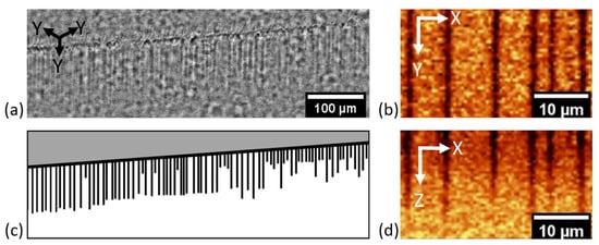
Figure 8.
Quasi-periodic structure of stripe domains growing during polarization reversal by series of short rectangular pulses of low field from a flat domain wall created in high field. (a) Optical image in transmitted light. Images obtained by CRM method: (b) in polar XY plane, (d) in XZ plane. (c) Schematic representation of quasi-periodic structure.
4. Discussion
The observed oriented growth of stripe domains can be explained within the framework of the kinetic approach to the domain structure evolution based on the analogy between the growth of domains and crystals. The driving force of the process in this case is the excess of the polar component of the local field (Eloc.z) over the threshold value [26]. The local field contains the contributions of: (1) a uniform external field (Eex) induced by the applied voltage, (2) a depolarization field (Edep) created by bound charges, depending on domain size and shape, (3) an external screening field (Eex.scr) created by the current in the external circuit, and (4) a bulk screening field (Eb) due to slow bulk screening processes.
where Erd.z (r, t) = Edep.z (r, t) − Eex.scr.z (r, t) is the residual depolarization field.
The motion of the domain wall is caused by the generation of the steps on the wall and the motion of the kinks along the wall [26]. The step generation velocity is determined by the excess of Eloc.z above the threshold value for generating steps Eth.st:
where ns is the concentration of steps, and k is the coefficient.
The kink motion velocity is determined by the excess of Eloc.z above the threshold value for the kinks’ motion Eth.k:
where µk is the mobility of kinks.
In a ferroelectric capacitor with an artificial dielectric layer, Erd.z is proportional to the ratio of the layer thickness Ld to the thickness of the sample d.
where εL and ε0 are dielectric permittivities of the dielectric layer and vacuum.
An increase in the (Erd.z − Eb.z) term in Equation (9) due to a retardation of the bulk screening leads to a spatially inhomogeneous Eloc on the domain wall and, as a result, to various shapes of growing polygonal domains [22]. Previously, it was shown that the calculated angular dependence Erd.z(φ) for a hexagonal domain had its minima at the domain vertices [26]. This result made it possible to explain the experimentally observed effect of “determined nucleation”, which is the generation of steps at the vertices of a polygonal domain [26]. A further increase in Erd due to a thicker dielectric layer leads to an Eloc decrease close to the threshold values. As a result, the steps’ generation and the kinks’ motion occur only at the vertexes of the stripe domains [26], which leads to their elongation without increasing the width.
To explain the process of the formation of the quasi-periodic structure of stripe domains upon changing the switching mode, the distribution of the excess of Eloc.z over Eth.st at the domain wall and the change in the moving wall shape (Figure 9) after the formation of a single ledge on it were numerically calculated [30].
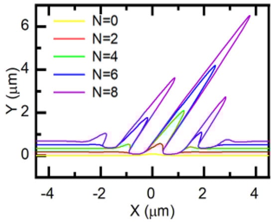
Figure 9.
Computer simulation of shape evolution of a moving domain wall for switching by the series of rectangular field pulses. N is the number of pulses.
The calculation was performed by the finite element method using the COMSOL Multiphysics software package. The effect of incomplete compensation of the bound charge on the surface behind the moving domain wall was taken into account. The local electric field on the domain wall was calculated at a depth of 400 nm. The change in the wall shape as a result of the application of the field pulse was obtained from the field dependence of the wall velocity according to Equation (2). Iterative calculation of the local field distribution and inhomogeneous domain wall shift made it possible to obtain the change in the wall shape during switching by a series of pulses. It is shown that quasi-periodic structures of ledges (stripe domains) are formed at the domain wall (Figure 9). The field decrease in the valleys between the ledges below the threshold ensures the existence of stable concave angles [30].
The orientation of the stripe domains in Y directions is due to the anisotropy of the domain growth velocity. The lower threshold fields for growth in the Y+ directions lead to anisotropic growth.
The abnormally low threshold fields for the stripe domains’ growth can be attributed to the influence of the composition gradient that appeared as a result of the SPE process. The gradient leads to the appearance of a “built-in” (bias) field, which facilitates the switching process and reduces the threshold field.
5. Conclusions
This paper presents the results of an experimental study of the abnormal evolution of the domain structure in lithium niobate single crystals of congruent composition with a surface layer modified by the SPE process. The study of the domain switching in a wide field range allowed two qualitatively different types of domain structure evolution to be revealed: (1) the growth of oriented stripe domains in the field range from 3.8 to 21.5 kV/mm and (2) the growth of hexagonal domains in the fields above 21.5 kV/mm. Imaging of the domain structure in the crystal bulk showed that the stripe domains were 4 µm wide and up to 30 µm deep. It was found that the stripe domains were oriented predominantly along three directions equivalent according to the LN symmetry (C3v) coinciding with the Y crystallographic directions. The time dependence of the total length of the stripe domains and the average effective domain structure period was analyzed for switching in an increasing field. It was shown that both dependencies could be analyzed within the framework of the modified Kolmogorov–Avrami approach, taking into account the transition from a one-dimensional β-model to a one-dimensional α-model. The possibility of creating a quasi-periodic structure of stripe domains by changing the switching mode from traditional to abnormal was demonstrated. In the fields of more than 21.5 kV/mm, extended flat domain walls were created, from which, in the fields of less than 21.5 kV/mm, a quasi-periodic structure of stripe domains grew. The length of the stripe domains was up to 100 µm, the depth was up to 20 µm, and the average period was about 5 µm.
The formation and growth of stripe domains were explained in terms of the kinetic approach to the evolution of the domain structure as a result of the domain wall motion under conditions of inefficient screening of the depolarization field caused by the presence of a modified surface layer in CLN SPE, which reduced the efficiency of fast external screening. The abnormally low threshold fields were attributed to the influence of an additional “built-in” field that facilitated the switching process due to a composition gradient created as a result of SPE.
Author Contributions
Conceptualization, V.S., A.A. and P.B.; formal analysis, E.S. and A.A.; methodology, H.T., F.D. and T.L.; investigation, E.S.; software M.K.; validation, V.S. and A.A.; supervision, V.S.; writing—original draft, E.S.; writing—review and editing, V.S. and A.A.; resources H.T., F.D., T.L. and P.B.; project administration, A.A.; funding acquisition, V.S. All authors have read and agreed to the published version of the manuscript.
Funding
The study was financially supported by the Ministry of Science and Higher Education of the Russian Federation within the Development Program of the Ural Federal University named after the first President of Russia B.N. Yeltsin in accordance with the program of strategic academic leadership “Priority-2030”.
Acknowledgments
The work was performed using the equipment of the Ural Federal University “Modern Nanotechnologies” (reg. No. 2968), supported by the Ministry of Science and Higher Education of the Russian Federation (Project 075-15-2021-677).
Conflicts of Interest
The authors declare no conflict of interest.
References
- Armstrong, J.A.; Bloembergen, N.; Ducuing, J.; Pershan, P.S. Interactions between light waves in a nonlinear dielectric. Phys. Rev. 1962, 127, 1918–1939. [Google Scholar] [CrossRef]
- Hum, D.S.; Fejer, M.M. Quasi-phasematching. Comptes Rendus Phys. 2007, 8, 180–198. [Google Scholar] [CrossRef]
- Shur, V.Y.; Rumyantsev, E.L.; Batchko, R.G.; Miller, G.D.; Fejer, M.M.; Byer, R.L. Domain kinetics in the formation of a periodic domain structure in lithium niobate. Phys. Solid State 1999, 41, 1681–1687. [Google Scholar] [CrossRef]
- Shur, V.Y.; Akhmatkhanov, A.R.; Baturin, I.S. Micro- and nano-domain engineering in lithium niobate. Appl. Phys. Rev. 2015, 2, 040604. [Google Scholar] [CrossRef]
- Yamada, M.; Nada, N.; Saitoh, M.; Watanabe, K. First-order quasi-phase matched LiNbO3 waveguide periodically poled by applying an external field for efficient blue second-harmonic generation. Appl. Phys. Lett. 1993, 62, 435–436. [Google Scholar] [CrossRef]
- Hadi, K.E.; Sundheimer, M.; Aschieri, P.; Baldi, P.; De Micheli, P.M.; Ostrowsky, P.B.; Laurell, F. Quasi-phase-matched parametric interactions in proton-exchanged lithium niobate waveguides. J. Opt. Soc. Am. B 1997, 14, 3197–3203. [Google Scholar] [CrossRef]
- Jackel, J.L.; Rice, C.E.; Veselka, J.J. Proton exchange for high-index waveguides in LiNbO3. Appl. Phys. Lett. 1982, 41, 607–608. [Google Scholar] [CrossRef]
- Korkishko, Y.N.; Fedorov, V.A. Relationship between refractive indices and hydrogen concentration in proton ex/changed LiNbO3 waveguides. J. Appl. Phys. 1997, 82, 1010–1017. [Google Scholar] [CrossRef]
- Korkishko, Y.N.; Fedorov, V.A.; Baranov, E.A.; Proyaeva, M.V.; Morozova, T.V.; Caccavale, F.; Segato, F.; Sada, C.; Kostritskii, S.M. Characterization of α-phase soft proton-exchanged LiNbO3 optical waveguides. J. Opt. Soc. Am. A 2001, 18, 1186–1191. [Google Scholar] [CrossRef]
- Lunghi, T.; Doutre, F.; Legoff, G.; Ayenew, G.; Tronche, H.; Tanzilli, S.; Baldi, P.; De Micheli, M. Soft-proton exchange on magnesium-oxide-doped substrates: A route toward efficient and power-resistant nonlinear converters. J. Appl. Phys. 2017, 122, 013103. [Google Scholar] [CrossRef]
- Chanvillard, L.; Aschiéri, P.; Baldi, P.; Ostrowsky, D.B.; De Micheli, M.; Huang, L.; Bamford, D.J. Soft proton exchange on periodically poled LiNbO3: A simple waveguide fabrication process for highly efficient nonlinear interactions. Appl. Phys. Lett. 2000, 76, 1089–1091. [Google Scholar] [CrossRef]
- Neradovskiy, M.M.; Shur, V.Y.; Mingaliev, E.A.; Zelenovskiy, P.S.; Ushakova, E.S.; Tronche, H.; Baldi, P.; De Micheli, M.P. Investigation of domain kinetics in congruent lithium niobate modified by proton exchange. Ferroelectrics 2016, 496, 110–119. [Google Scholar] [CrossRef]
- Shur, V.Y.; Akhmatkhanov, A.R.; Chuvakova, M.A.; Dolbilov, M.A.; Zelenovskiy, P.S.; Lobov, A.I. Formation of self-organized domain structures with charged domain walls in lithium niobate with surface layer modified by proton exchange. J. App. Phys. 2017, 121, 104101. [Google Scholar] [CrossRef]
- Gustavo, R.P.; David, D.T.; Gabriel, B.; Blanton, T.; Lee, S.T.; Salter, L.M. Characterization of proton exchange lithium niobate waveguides. J. Appl. Phys. 1994, 76, 3981. [Google Scholar] [CrossRef]
- Zelenovskiy, P.S.; Fontana, M.D.; Shur, V.Y.; Bourson, P.; Kuznetsov, D.K. Raman visualization of micro- and nanoscale domain structures in lithium niobate. Appl. Phys. A 2010, 99, 741–744. [Google Scholar] [CrossRef]
- Shur, V.Y.; Kuznetsov, D.K.; Mingaliev, E.A.; Yakunina, E.M.; Lobov, A.I.; Ievlev, A.V. In situ investigation of formation of self-assembled nanodomain structure in lithium niobate after pulse laser irradiation. Appl. Phys. Lett. 2011, 99, 082901. [Google Scholar] [CrossRef]
- Li, C.H.; Lee, C.K. Minimum cross entropy thresholding. Pattern Recognit. 1993, 26, 617–625. [Google Scholar] [CrossRef]
- Bradski, G. The OpenCV library. Dr. Dobb’s. J. Softw. Tools 2000, 120, 122–125. [Google Scholar]
- Virtanen, P.; Gommers, R.; Oliphant, T.E.; Haberland, M.; Reddy, T.; Cournapeau, D.; Burovski, E.; Peterson, P.; Weckesser, W.; Bright, J.; et al. SciPy 1.0: Fundamental algorithms for scientific computing in Python. Nat. Methods 2020, 17, 261–272. [Google Scholar] [CrossRef]
- van der Walt, S.; Schönberger, J.L.; Nunez-Iglesias, J.; Boulogne, F.; Warner, J.D.; Yager, N.; Gouillart, E.; Yu, T. Scikit-image: Image processing in Python. PeerJ 2014, 2, e453. [Google Scholar] [CrossRef]
- Hunter, J.D. Matplotlib: A 2D graphics environment. Comput. Sci. Eng. 2007, 9, 90–95. [Google Scholar] [CrossRef]
- Kolmogorov, A.N. On the Statistical Theory of Crystallization of Metals. Izv. Acad. Nauk USSR Ser. Math. 1937, 3, 355–359. [Google Scholar]
- Avrami, M. Kinetics of phase change. I General theory. J. Chem. Phys. 1939, 7, 1103–1112. [Google Scholar] [CrossRef]
- Shur, V.Y.; Rumyantsev, E.L.; Makarov, S.D. Kinetics of phase transformations in real finite systems: Application to switching in ferroelectrics. J. Appl. Phys. 1998, 84, 445–451. [Google Scholar] [CrossRef]
- Ishibashi, Y.; Takagi, Y. Note on ferroelectric domain switching. J. Phys. Soc. Jpn. 1971, 31, 506–510. [Google Scholar] [CrossRef]
- Shur, V.Y.; Pelegova, E.V.; Kosobokov, M.S. Domain shapes in bulk uniaxial ferroelectrics. Ferroelectrics 2020, 569, 251–265. [Google Scholar] [CrossRef]
- Damjanovic, D.; Demartin, M. The Rayleigh law in piezoelectric ceramics. J. Phys. D Appl. Phys. 1996, 29, 2057. [Google Scholar] [CrossRef]
- Volk, T.; Wöhlecke, M. Lithium Niobate; Springer: Berlin/Heidelberg, Germany, 2008; ISBN 978-3-540-70766-0. [Google Scholar]
- Esin, A.A.; Akhmatkhanov, A.R.; Shur, V.Y. Superfast domain wall motion in lithium niobate single crystals. Analogy with crystal growth. Appl. Phys. Lett. 2019, 114, 192902. [Google Scholar] [CrossRef]
- Shur, V.Y.; Mingaliev, E.A.; Kosobokov, M.S.; Nebogatikov, M.S.; Lobov, A.I.; Makaev, A.V. Self-assembled shape evolution of the domain wall and formation of nanodomain wall traces induced by multiple IR laser pulse irradiation in lithium niobate. J. Appl. Phys. 2020, 127, 094103. [Google Scholar] [CrossRef]


Disclaimer/Publisher’s Note: The statements, opinions and data contained in all publications are solely those of the individual author(s) and contributor(s) and not of MDPI and/or the editor(s). MDPI and/or the editor(s) disclaim responsibility for any injury to people or property resulting from any ideas, methods, instructions or products referred to in the content. |
© 2023 by the authors. Licensee MDPI, Basel, Switzerland. This article is an open access article distributed under the terms and conditions of the Creative Commons Attribution (CC BY) license (https://creativecommons.org/licenses/by/4.0/).