1. Introduction
Quasi-phase matched (QPM) non-linear optical materials are promising candidates for producing tunable and powerful laser sources in the mid-infrared (IR) and terahertz (THz) region, essential for sensing gasses, explosives, and biological agents, and for applications such as military infrared countermeasures, medical imaging, industry, and spectroscopy [
1,
2,
3,
4]. OP-GaP is a potential QPM material with higher thermal conductivity, lower thermal expansion coefficient, and negligible two-photon absorption (2PA) when compared with GaAs. Due to the lower 2PA, OP-GaP enables efficient pumping with high power near IR laser sources at the wavelengths of 1040 nm and 1064 nm to obtain high output power in the mid-IR region [
5,
6]. The OP templates are usually prepared by either epitaxial inversion, a molecular beam epitaxy (MBE) assisted polarity inversion technique, or by the wafer bonding method. To start with, in the former method, a non-polar silicon layer deposited by MBE on a GaP wafer is used to grow, also by MBE, the inverted GaP layer. In contrast, in the latter method, two oppositely oriented GaP wafers are bonded together. In both cases, subsequent lithography and selective etching techniques are used to produce the periodic patterns of alternating crystal domains with nonlinear susceptibility χ
(2) [
7,
8,
9]. However, the commercially available GaP is expensive and, in addition, it has lower structural and surface quality compared to the commercial GaAs substrate [
10]. As a consequence, OP-GaP templates turn out to be a poor starting material for producing good quality thick OP-GaP. Thus, OP-GaAs templates are a better choice for this purpose, despite the relatively large lattice mismatch of −3.57% between GaP and GaAs. In this work, OP-GaP layers have been grown heteroepitaxially on OP-GaAs templates using HVPE [
11]. OP-GaAs templates were prepared using either the MBE-assisted epitaxial inversion [
2] or the wafer bonding method [
12]. It was found that a comparative study on the heteroepitaxial OP-GaP growth on OP-GaAs templates produced using both methods is limited, despite existing growth studies on these individual templates [
2,
13]. We studied the influence of these two types of templates on the crystalline quality of the grown OP-GaP domains in respect to fidelity and growth rate. Domain fidelity denotes the preservation of orientation pattern from the template (OP-GaAs) to the OP-GaP layers with intact boundaries (domain boundaries) between the domains with the opposite orientation. To this end, we adopted high-resolution x-ray diffraction reciprocal space maps. We indicate the potential use of this technique hereby exploited for this purpose for the first time. Because OP-ZnSe is also becoming an attractive material for QPM due to its small lattice mismatch of +0.26% between ZnSe and GaAs, besides its excellent optical properties [
3], we included this material in this study to demonstrate the usefulness of HRXRDRSM in establishing the crystal quality of individual domains and domain fidelity. We propose from this study that once the growth rate is optimized from SEM studies, HRXRDRSM analysis alone can be used to assess the crystalline quality and to infer the domain fidelity of the OP structures.
2. Materials and Methods
OP-GaP epitaxial films were grown using a horizontal low-pressure HVPE reactor on epitaxial inversion and wafer-bonded OP-GaAs templates. GaCl and PH3 were used as the precursor for Ga and P, respectively. GaCl was formed in situ through the reaction between high purity (6N grade) molten gallium in the quartz boat placed in the source zone of the reactor and HCl gas, at around 740 °C. N2 was used as the carrier gas. The precursors were mixed at the gas mixing zone (between source and deposition zones) and the growth took place on the templates/substrates at the deposition zone. The reactor pressure and total gas flow were maintained at 20 mbar and 900 sccm, respectively, for all the growths. An amount of 45 sccm of H2 was used in all growths, which was 5% of the total flow.
OP-GaAs templates were prepared by the MBE polarity inversion technique (at BAE Systems, Inc. and AFRL) and by wafer bonding (at Thales Research and Technology), as the polarity of GaAs was flipped by growing it on a non-polar Ge layer in the former method, and the fabrication process can be found in [
2], whereas two oppositely oriented GaAs wafers were bonded to form OP-GaAs template in the latter method; the template preparation steps are described in [
12]. The schematic of MBE-grown and wafer-bonded OP-GaAs templates with the orientation of substrate domain (+) and inverted domain (-) is depicted in
Figure 1. The width of each domain is about 30 µm on both OP-GaAs templates.
To identify the optimum growth condition to achieve high growth rate and retain domain fidelity in the OP-GaP growth, five runs were conducted by varying the precursor flow and V/III ratio, hereinafter called OG-1, OG-2, OG-3, OG-4, and OG-5. In all five growth runs, four substrates/templates were loaded, which are (i) MBE-grown OP-GaAs template, (ii) wafer-bonded OP-GaAs template, (iii) (001) GaAs substrate, and (iv) (001) GaP substrate. The planar (001) substrates were used as references to monitor the variation of growth rates in each run. For the OG-4 run, 5 sccm of HCl (excess flow) diluted with 250 sccm of N
2 was injected into the reactor chamber to suppress the parasitic reactions and to study its effect on the growth rate of OP-GaP on the templates. All four samples in each run were subjected to temporally resolved growth at the optimized substrate temperature of 710 °C with alternating layers of unintentionally-doped GaP (UID-GaP) (each time for 8 min) and sulfur (S)-doped GaP (GaP:S) (each time for 2 min). This temporally resolved growth was adopted to investigate the emerging domain boundaries in the grown OP-GaP layers. Hydrogen sulfide (H
2S) was used as the precursor for S. The growth time for OG-1 to 4 runs was kept at 40 min. The OG-5 run was targeted to grow a thicker OP-GaP layer for 90 min to probe the effect of a lower V/III ratio of 2 on the growth rate and domain fidelity on both templates. Hereafter, the OP-GaP layer grown on the OP-GaAs template made by MBE is denoted as M, and on the OP-GaAs template made by the wafer bonding method is denoted as W.
Table 1 summarizes the growth parameters of all the five runs.
The samples were characterized by the HRXRDRSM along (004) reflections using the PANalytical Empyrean HRXRD tool. The preparation of OP templates involves MBE or wafer bonding, which makes them expensive, time-consuming, and challenging. In addition, the subsequent growth of thick OP-GaP or other OP materials using HVPE requires several hours of growth to achieve a large enough optical aperture. Considering all these laborious processes involved in the preparation of the OP materials, we tried to analyze these OP-GaP structures using the non-destructive HRXRDRSM technique to assess the crystalline quality of their individual domains and to infer the domain fidelity [
14]. The destructive cross-sectional analysis, however, adds complete information on the domain fidelity and growth rate. The cross-sectional surface of OP-GaP on OP-GaAs samples were stain etched in (1:1) orthophosphoric acid + H
2O
2 mixture before SEM analysis to distinguish the sulfur-doped OP-GaP and undoped OP-GaP as well as to resolve the domain boundaries. We propose from this study that once the growth rate is optimized from SEM studies, HRXRDRSM analysis alone can be used to assess the crystalline quality and to infer the domain fidelity of the OP structures.
In addition to the above OP-GaP samples, an OP zinc selenide (OP-ZnSe) sample grown on an OP-GaAs template made by MBE has also been included in this HRXRDRSM analysis to investigate the applicability of this heteroepitaxial technique on another material system. The OP-ZnSe was grown on an OP-GaAs template by the HVPE technique at AFRL, USA. The detailed growth procedure can be found in [
3,
15].
3. Results
Figure 2a–d depict the (004) HRXRDRSM of OP-GaP grown on samples M1, W1, M2, and W2. It is worth noting that the two peaks exhibited in the HRXRDRSM contour correspond to the substrate-oriented domain (OD) and the inverted domain (ID) of the OP-GaP layer.
Figure 2a shows two tiny contours above the substrate contour (OP-GaAs). These are indicative of the OP-GaAsP transition or intermediate layer that could have formed due to the phosphorus adatoms incorporation during the initial growth stage on the OP-GaAs substrate. However, the presence of such a transition layer was not evident in the rest of the OP-GaP samples grown on either MBE (M) or wafer-bonded (W) OP-GaAs templates. The contour shape of OD and ID for M1 is almost identical in
Figure 2a, with a small enlargement along the Qz direction for the former and in the Qx direction for the latter domain, respectively. The full width at half maximum (FWHM) value reveals the crystalline quality of the OP-GaP layer. The FWHM values for both the OD and ID of OP-GaP have been calculated from the HRXRDRSM and it was found to be 158 and 219 arcsec, respectively, for sample M1. The omega angle separation (Δω) between the domains is 0.21° (756 arcsec).
Figure 2b depicts the well-separated contours of OD and ID of sample W1. The OD contour has been slightly elongated in the Qx and Qz directions when compared to that of ID. The angular separation between the domains in the omega axis, Δω, was found to be 0.3° (1080 arcsec). The FWHM of OD and ID has been extracted from the HRXRDRSM as 212 and 204 arcsec.
Figure 2c shows the (004) HRXRDRSM of the OP-GaP samples grown on an MBE template (M2). The contour of OD and ID are not similar for the sample M2; the OD contour has been elongated in the Qz and that of ID has been broadened along the Qx directions. The FWHM values of OD and ID of OP-GaP are 182 and 362 arcsec, respectively. The Δω between the domains is 0.24° (864 arcsec).
Figure 2d shows the OP-GaP contours of (001) OD and (00-1) ID of the sample W2. The shape of the OD contour has been found more elongated in the Qx direction. The Δω between the domains is found to be wider than the W1 sample, 0.38° (1368 arcsec). The FWHM of OD and ID of sample W2 is 246 and 226 arcsec.
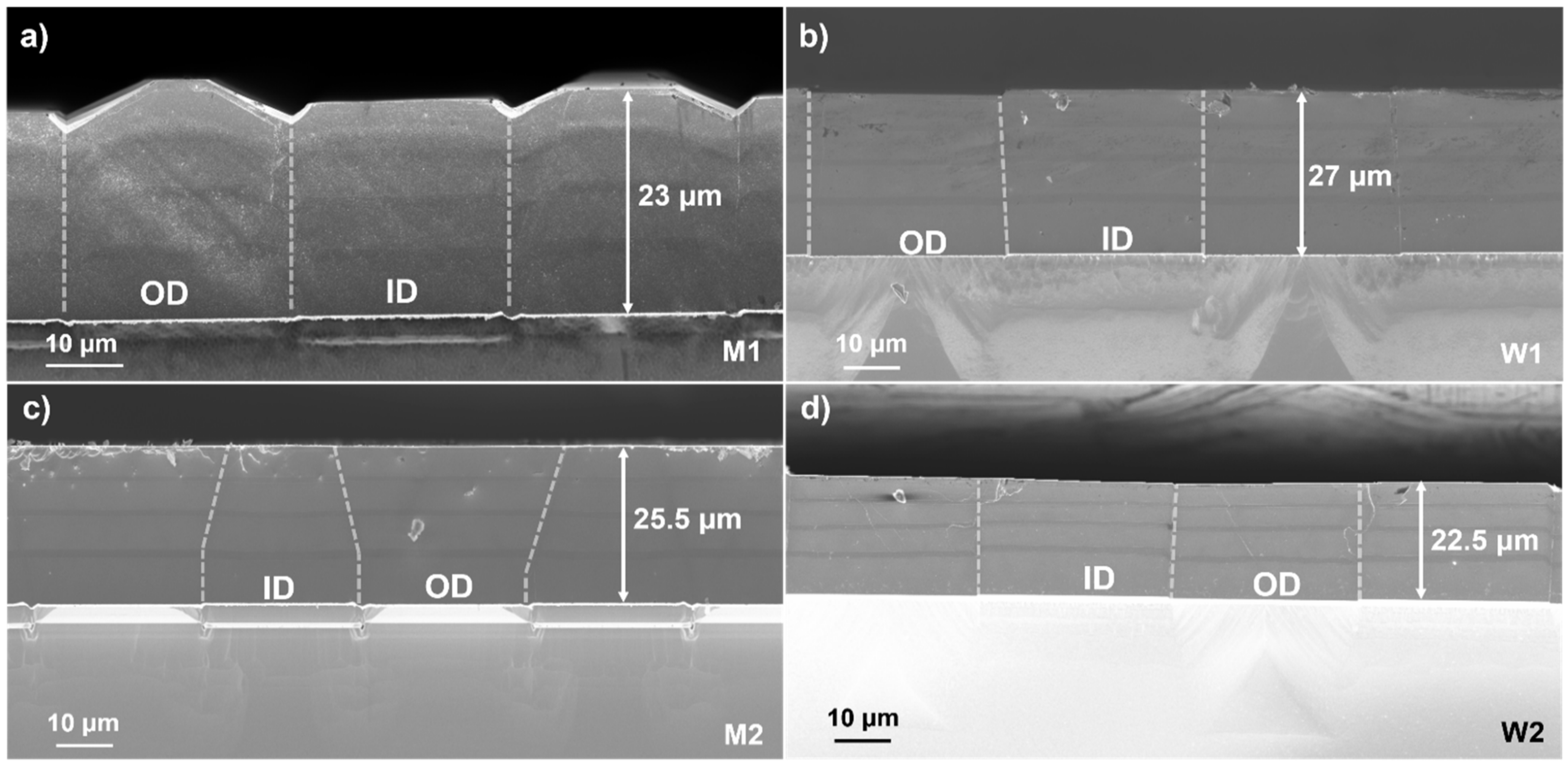
The cross-sectional SEM images of OP-GaP from runs OG-1 and OG-2 in
Figure 3 reveal (along the layer thickness) the four periods of unintentionally-doped GaP and S-doped GaP layers, as expected.
In all the cross-sectional images, the domain boundaries between ODs and IDs are highlighted with the dotted lines as a guide, and the thickness of each sample has been marked. The domain boundaries are intact between OD and ID with excellent domain fidelity in sample M1, as shown in
Figure 3a. The thickness of OP-GaP in sample M1 is 23 µm. In
Figure 3b (sample W1), the domain boundaries are visible and exhibit good domain fidelity with a thickness of 27 µm.
Figure 3c (sample M2) reveals that the width of the IDs is getting narrower with the increasing thickness of the grown OP-GaP layer, whereas that of the ODs is becoming wider. This may lead to the pinch-off of IDs after a certain thickness if the growth continued for a longer duration. The domains maintain their fidelity for the first few minutes of growth, but at the end of the first of the four periods, the IDs start to shrink when compared with the ODs. The thickness of this OP-GaP layer (M2) is 25.5 µm. In contrast, just like sample W1, OP-GaP on sample W2 maintains the domain fidelity with the thickness of 22.5 µm, as seen in
Figure 3d. The growth rate is slightly reduced in this case (W2) concerning M1, W1, and M2.
HRXRDRSM of OP-GaP (sample M3) in
Figure 4a exhibits the difference in the domains contour shape; however, unlike the cases presented in
Figure 2, the separation between the OD and ID is less distinct; in addition, the positions of OD and ID are interchanged with respect to the substrate peak. The OD contour is elongated along the Qz direction like that of sample M2 (see
Figure 2c) and that of ID in the Qx direction.
The separation of the domain peaks in the omega axis, Δω, is 0.18° (648 arcsec). The FWHM of OD and ID is 199 and 315 arcsec, respectively. For sample W3 (
Figure 4b), the positions of the OD and ID contours are also interchanged as for M3. However, the variation in the shape of contours is more pronounced in W3, unlike in the cases of W1 and W2 (see
Figure 2b,d). The OD contour is expanded towards the Qx direction, and the ID contour is expanded towards the Qz direction. The FWHM of the OD and ID is calculated as 196 and 190 arcsec, with an Δω of 0.28° (1008 arcsec) between the domains in the omega direction.
Figure 4c shows that the OD and ID contours of M4 are not like those of sample M3, and the separation between the domains is apparent. However, the position of OD and ID in M4 are interchanged as in M3. As in the other Mx’s samples, the shape of the OD contour is well defined, and it appears to be elongated slightly along the Qz direction, whereas the ID contour is stretched out more in the Qx direction. The shape of the ID contour is not well pronounced, and the separation between the domains in the omega axis, Δω, is 0.182° (655 arcsec). The FWHM of OD and ID is 168 and 413 arcsec, respectively. The HRXRDRSM of OP-GaP of W4 shows a noticeable difference in the shape of the OD and ID contours, with an Δω of 0.38° (1368 arcsec), as noticed in
Figure 4d. Unlike the previous three samples (W1, W2, and W3) the OD contour of W4 is extended in the Qz direction and that of ID is drawn out in the Qx direction. The FWHM of OD and ID is 189 and 210 arcsec, respectively.
The cross-sectional SEM images in
Figure 5 disclose the boundaries between the domains for samples M3, W3, M4, and W4. It is interesting to observe from
Figure 5a that the domains maintain their fidelity after the first or second period of growth of OP-GaP, despite the initial deterioration in sample M3. The thickness of the OP-GaP layer increased to 32 µm compared to sample M2 (25.5 μm).
The domain boundaries between ODs and IDs of OP-GaP in sample W3 and W4 shown in
Figure 5b,d exhibit certain tapering. This phenomenon was there even in the corresponding samples in the growth runs of OG-1 and OG-2. The thickness of the grown layer in the W3 samples has been measured as 31 µm.
Figure 5c shows that in the first few minutes the domains followed the OP-GaAs template pattern, but later, until the completion of the first period of growth, the ODs started to expand, and the IDs begin to shrink in sample M4, and the domain boundaries remain vertical from the second period. Furthermore, it is worth noting that fidelity is preserved from the beginning to the end of the growth between a few of the ODs and IDs. The introduction of excess HCl seems to improve the fidelity, with no reduction in the growth rate of OP-GaP in sample M4. Its thickness is 32 µm. On the other hand, the excess HCl reduced the growth rate of OP-GaP in sample W4. Its thickness is now only 25 µm, which is lower than that of W3 (31 µm).
The HRXRDRSM on samples M5 and W5 from the OG-5 run are shown in
Figure 6.
Figure 6a shows the OP-GaP contour of the M5 sample. We can observe only the OD contour with a slight expansion towards the side of the ID contour, and the ID contour is completely missing. The OD contour has nicely spread over the Qz and Qx directions. Because there was no contour for the ID, most probably it should not have reached the surface (which can be seen in
Figure 7a). The FWHM of OD of M5 is 154 arcsec. In
Figure 6b, for sample W5, the OD can be seen to spread over the Qz direction, whereas a small signal or contour has been obtained for the ID besides that of OD. This is an indication of poor domain fidelity (also indicated in
Figure 7b) and crystalline quality. The FWHM of OD and ID of sample W5 is 180 and 1428 arcsec. The Δω between OD and ID in the omega axis is found to be 0.27° (972 arcsec).
In line with the above HRXRDRSM analyses, the cross-sectional SEM image in
Figure 7a clearly confirms that the ID in the OP-GaP layer of sample M5 is pinched off and only the ODs have grown vertically and laterally at the expense of IDs. Likewise,
Figure 7b exhibits the poor domain fidelity between ODs and IDs; the IDs just managed to reach the surface, and as a result, we can see a small contour for ID in the HRXRDRSM image. Moreover, the thickness of the OP-GaP grown on MBE and wafer-bonded OP-GaAs is 65 and 50 μm, respectively.
Figure 8 shows the HRXRDRSM of OP-ZnSe on the OP-GaAs template. The contours of the GaAs substrate, OD, and ID of OP-ZnSe are obtained from the HRXRDRSM. The thickness of OP-ZnSe is 22 μm. The ZnSe lattice constant is slightly higher than the GaAs lattice constant, hence the substrate GaAs contour is seen above the OP-ZnSe layer. The FWHM of OD and ID of OP-ZnSe is found to be 241 and 520 arcsec, respectively. The Δω between the domains in the omega axis is noted to be 0.29° (1044 arcsec).
As one can see on the next SEM cross-section image of the OP-ZnSe sample (
Figure 9), the domain fidelity is slightly disturbed by the wider and narrower growth of the domains with the opposite orientation. HRXRDRSM in
Figure 8 indicates the fluctuations in the domain fidelity for the OP-ZnSe on the OP-GaAs template clearly, much like that of OP-GaP on the OP-GaAs template.
4. Discussion
The HRXRDRSM of (004) reflection of all the samples, Mx’s and Wx’s (with x = 1 to 5), revealed the contours of the substrate, and two peaks that are originated from OP-GaP. Because the substrate-oriented domain (OD) is epitaxially grown on the substrate, the deviation between the OD and the substrate is expected to be lower than that between the ID and the substrate, which is used to identify OD and ID peaks in HRXRDRSM for all the investigated OP-GaP layers. In addition, the shapes of the contours indicate the changes in the domain boundary. As seen in
Figure 2a the HRXRDRSM of OD and ID of OP-GaP (sample M1) exhibit well-shaped contours with a small stretch along the Qz and Qx directions. A similar spread of the OD contours along the Qz direction and ID contours along the Qx direction has been observed, to a noticeable extent in the samples M2, M3, and M4, as seen in
Figure 2c and
Figure 4a,c. The spread over the Qz and Qx directions indicates strain in the growth direction and deformation along the in-plane of the samples [
16].
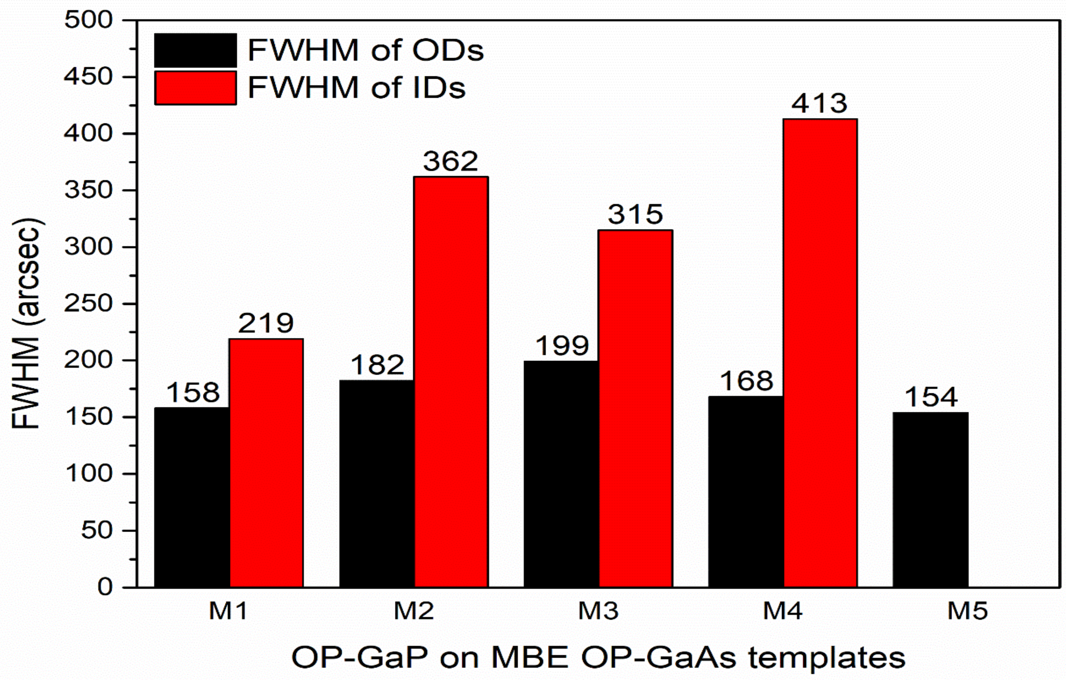
The FWHM of ODs and IDs calculated from the OP-GaP HRXRDRSM of the M1–M5 samples is shown in
Figure 10. The FWHM values of ODs and IDs indicate that the crystal quality of ODs is better than that of IDs for the OP-GaP layers grown on the MBE OP-GaAs template. Notably, the crystal quality of the domains is reflected in the contour shapes with the spread of the ODs and IDs contour along the Qz and Qx directions. Because only the ODs have been grown predominantly by suppressing the IDs growth in M5, we obtained only the OD contour in M5. How the ODs overgrow the IDs is also shown in
Figure 7a.
The FWHM of ODs and IDs calculated from the OP-GaP HRXRDRSM of W1–W5 samples is shown in
Figure 11. The FWHM of OD and ID is comparable in W1–W4, unlike that of the Mx’s and W5 samples.
From the HRXRDRSM of all the samples, it is confirmed that the contours of the domains that spread over the Qx direction have wider FWHM, which can be ascribed to the in-plane deformations; likewise, if they spread over the Qz direction, the FWHM of the domains are narrow, which is ascribed to strain along the growth direction. In all the OP-GaP layers grown on the MBE OP-GaAs template (M1–M4), the crystalline quality of the IDs is lower than that of the ODs, which is ascribed to the imbalance in the growth of IDs for M2, M3, and M4. However, the ID quality is relatively lower in the M1 sample than that of OD, wherein the domain fidelity is predominant throughout the growth. The possibility of the lower crystal quality of the original inverted GaAs layer grown on a non-polar Ge layer in Mx’s when compared with the GaAs substrate used for the template preparation may contribute to the reduction in the quality of IDs in Mx’s. On the contrary, mostly in the OP-GaP layers of Wx’s sample, the crystalline quality of the ODs is comparable to that of the IDs. This may be attributed to the better quality of the inverted GaAs layer in the wafer-bonded template. In the case of W5, OD is better than the ID in crystal quality. The ID peak was very weak due to the unbalanced growth and poor crystal quality. These observations lead us to understand the importance of fine tuning the HVPE growth parameters to obtain domain fidelity and crystal quality in the OP-GaP layers, regardless of OP-GaAs template quality.
The cross-sectional SEM images (
Figure 3,
Figure 5 and
Figure 7) depict the domain boundaries and thickness of the samples in OG-1 to 5. The variations in the growth rate of the GaP layers grown on the two types of OP-GaAs templates and on the planar GaAs and GaP substrates are shown in
Figure 12.
To explain the drawings in
Figure 12 let us return to the cross-section images shown before. For example,
Figure 3a clearly shows the fidelity of domains in M1, which confirms the findings from their HRXRDRSM contours, shown in
Figure 2a. Moreover, it is noted that the ODs are bounded by the {111}A planes laterally and with the {100} planes on the surface. Here the growth rates of both the domains are equal (35 μm/h), although there is some faceting of ODs. As regards Wx’s, the original patterns are replicated substantially in the ODs and IDs, with almost no faceting. In W1 (
Figure 3b), the growth rate was 41 μm/h, higher than its counterpart, M1. The increase in the growth rate can be explained either by the availability of additional bonding sites due to the high density of atomic terraces in the wafer-bonded template [
9], because 2° off (001) GaAs substrates were used for this purpose, or it might be due to the effective de-chlorination of the template surface by the atomic hydrogen released at the thermal decomposition of the PH
3 atoms [
17]. The latter seems to be more effective in determining the growth rate than the former because the MBE-made GaAs templates were also prepared using (100) GaAs wafers with 4° miscut towards the (111)B direction. To increase the rate of desorption of chlorine from the growing layer surface and thereby increase the growth rate of OP-GaP layers, the PH
3 flow was increased. Thus, the V/III ratio was increased from 5 in OG-1 to 10 in OG-2. This resulted in an increase in the growth rate of 38 µm/h in M2 from 35 µm/h in M1, and concomitantly, the ID was shrunk and OD became wider due to the difference in the growth rate along the lateral and vertical directions, respectively; see
Figure 3c. This figure also reveals that while increasing the V/III ratio the IDs became bounded by the lower growth rate {111}B planes [
18]; furthermore, the faceting of the domains seen in
Figure 3a almost disappeared, and the fidelity of the domains deteriorated. On the other hand, as seen in
Figure 3d, the growth rate of W2 dropped to 34 μm/h from 41 µm/h for W1, which was not anticipated. It is possible that, during the pyrolysis of PH
3, the formation of molecular P
2 reduces the growth rate as it would not efficiently react with Ga adatoms such as the atomic P [
19], or the Ga precursor might be insufficient. However, the growth rate increased in M2 and decreased in W2, the former could be partly attributed to the 4° off (100) GaAs substrate, which has more bonding sites than the latter. The reaction mechanism between the precursors adatom is noted to differ with the type of the OP-GaAs templates.
Further to increasing the growth rate of the OP-GaP layer to achieve a thickness of a few hundred microns required for frequency conversion devices (FCD), the GaCl flow was increased from 10 sccm in OG-2 to 20 sccm in OG-3, although this might cause certain parasitic deposition on the reactor wall. In this case, by increasing the III-group element flow the V/III ratio was brought down to 5. As a result, the growth rate jumped to 48 and 47 μm/h for M3 and W3, respectively. This indicates that an increase in supersaturation increases the growth rate [
19]. Further,
Figure 5a shows that the domain fidelity is revived after the first or second period. The appearance of {111}A planes prevented the IDs from pinching off, which is elucidative at the surface of IDs. The IDs bounded by the {111}A planes are preserved from further narrowing down.
Figure 5b also reveals the presence of a higher growth rate of {111}A planes bounding the IDs, which can be seen clearly at the surface of the IDs. The balance between the chemisorption of Ga and P adatoms and the desorption of chlorine and hydrogen in the form of HCl eventually increases the growth rate [
20]. The introduction of the excess flow of HCl into the reactor in the run OG-4 did not change the growth rate of M4 from M3 but reduced it to 38 μm/h in W4 when compared to 47 μm/h for W3. The excess HCl seems to improve the domain fidelity a little in the M4 with respect to M3, by balancing the absorption of Ga and P adatoms over both domains; in addition, the {111}A planes also surround the IDs, as seen in
Figure 5c. In the case of W4, the excess of HCl should have reduced the de-chlorination process, and as a result growth rate is reduced. In M5 and W5, the growth rate of GaP is found to be 43 μm/h and 33 μm/h, respectively. Compared to the growth rate of the M1 and M2 samples, the growth rate of the GaP layer on the M5 is higher, and it is lower than that of M3 and M4. On the other hand, W5 records the lowest growth rate when compared with the W1–4 samples. This observation indicates that an optimal V/III ratio with the balance between III and V group precursors is essential to increase the growth rate and preserve domain fidelity. Otherwise, the reduction in the de-chlorination, generation of molecular P
2, and parasitic deposition reduce the growth rate. The disparity in the growth rate between the ODs and IDs aggravates the domain fidelity. It is interesting to note that the conversion efficiency of GaCl into GaP is calculated to be ~8% for the growth rate of 40µm/hour on a 50 mm diameter wafer using the average flow of 15 sccm of GaCl.
As shown in
Figure 12, larger differences in layer thickness are observed between W1 and W2 when the V/III ratio is increased and between W3 and W4 when excess HCl is introduced, as compared to the corresponding growths on MBE-assisted epitaxial inversion templates. The wafer-bonded templates have been prepared using 2° off (001) GaAs substrates and the MBE-made OP GaAs templates using (100) GaAs wafers with 4° miscut towards the (111)B direction. It appears that, in the latter case, the existence of more bonding sites for the Ga and P adatoms (local surface kinetics) eventually determines the growth rate. Hence, growth rates of M1 and M2, as well as M3 and M4, are not largely affected by the gas input ratios. In the case of wafer-bonded templates, these bonding sites are less than those in the MBE-assisted templates. Here the local surface kinetics appear to be less dominant, and the gas input ratios influence the growth rate somewhat to a larger extent. The difference between OG-1 and OG-2 is the increase in the V/III ratio twice, which results in a decrease in the growth rate of W2 with respect to W1 because GaCl is largely the rate growth rendering species. The difference between OG-3 and OG-4 is the presence of excess HCl in the latter, which decreases the supersaturation, resulting in lower growth rate in W4 with respect to W3.
The growth rate of GaP on the planar GaAs and GaP substrates varies with runs. It varies from 0 to 30% when compared with the growth rate of GaP on OP-GaAs templates. Notably, the GaP layer growth rate is higher on the GaAs substrate than on the homoepitaxial GaP substrates in all five runs. This could be attributed to higher threading dislocations in heteroepitaxy enhancing the growth rate in the former as per the BCF model of crystal growth [
21]. The M5, W5, and OP-ZnSe samples have been used to test the potential of HRXRDRSM. The ID contour in the OP-ZnSe on OP-GaAs template is not pronounced as well as that of OD. Both the domains’ contours have been spread predominantly along the Qx direction. The OD contour is slightly stretched out in the Qz direction compared with that of ID. The HRXRDRSM (
Figure 8) and the SEM cross-section image (
Figure 9) of the grown OP-ZnSe reveals that both the domains reached the surface but not with the best domain fidelity.
Figure 13 shows the schematic of the possible arrangement of OP-GaP or OP-ZnSe domains on the template and the Δω. As per the model of the mosaic crystal, the epilayer is composed of mosaic blocks. If the block size is more than a few microns, individual mosaic blocks may be isolated and imaged in the RSM [
16]. Here, each domain (OD and ID) is considered as a mosaic block, and they are about 30 μm wide, and there is some misorientation between them, which is obtained as angular separation (Δω) in the omega axis of HRXRDRSM. Because the tilts and strains are naturally separated in RSM, we could observe the OD and ID of the OP-GaP layer and the OP-ZnSe layer if they reach the surface.

 ,
, 


