1. Introduction
The concept of photonic crystals was proposed in 1987 by both Eli Yablonovitch [
1] and Sajeev. John [
2] when they studied periodic dielectric materials. Photonic crystal is a structure composed of alternating stacks of layers with different refractive indices [
3,
4,
5,
6]. The most important characteristic of photonic crystal is the existence of a photonic band gap in certain frequency regimes. Light or electromagnetic waves of any frequency located in the band gap region are unable to propagate [
7,
8]. Photons can be controlled and manipulated effectively by using the photonic band gap. Similar to the semiconductor band structure, when a defective layer is inserted into a photonic crystal, corresponding defective levels will be generated in the photonic band gap, which will significantly change the optical properties of the photonic crystal. In photonic crystals with a defective layer, owing to the destruction of the original periodicity or symmetry, a defect state with a very narrow frequency range may appear in the photonic crystal band gap, which is the so-called defect mode. The defect mode will lead to the localization of the photon and the photon is localized at the defect where the energy of the electromagnetic field is highly concentrated. The defect mode is a resonance mode with high transmittance and low reflectance. Photonic crystals have a wide range of applications in integrated optics, microwave communication and other fields due to these characteristics [
9,
10,
11,
12,
13,
14,
15,
16,
17,
18,
19,
20,
21,
22,
23].
The geometry of the structure and the dielectric indices of the component materials affect the photonic band gaps. If the geometry is determined, the photonic band gaps can only be changed by changing the component materials. A lot of work has been done to calculate photonic band gaps with different components. Photonic crystals composed of ordinary media [
18,
19,
20,
21,
22,
23,
24], semiconductors [
17,
25], and metals [
26,
27] have been carried out extensively and deeply. These conventional materials will have some shortcomings; for example, they will inevitably encounter the inherent loss caused by metallic extinction coefficient in the application of a metallic photonic crystal. To overcome this loss problem, a variety of non-conventional materials have also been used to construct photonic crystals. A photonic crystal which is composed by these materials usually presents some special properties in the photonic band gap due to the special optical properties of these materials. Photonic crystals composed of superconductors [
28] have started to attract widespread interest in recent years. Compared with metal photonic crystals, superconductivity has the advantages of low loss and adjustable permittivity. The electromagnetic wave in a superconductor is dependent on the London penetration depth, which is a function of temperature and external magnetic field in which the permittivity of the photonic crystal is tunable. Many researchers use superconductors and materials with different refractive indices to compose various superconductor photonic crystals to prepare new photonic crystal application devices. Pei et al. [
29] designed a tunable Mach–Zehnder interferometer with a two-dimensional photonic crystal structure using the superconductor. They have shown that different temperature distributions can lead to a significant change in the light transmission. Aly et al. [
30] found a cutoff frequency by calculating the transmittance spectra at THz of a one-dimensional superconducting nanomaterial-dielectric superlattice. Lee and Wu [
31] numerically analyzed the influence of temperature on the transmission spectrum in the visible light range in the one-dimensional low-temperature superconductor-dielectric photonic crystal. Ordinary liquid thermometers no longer work properly when the temperature drops to near absolute zero. Therefore, special temperature sensors with high sensitivity are required to measure the extremely low temperature in cryogenic environments. When the temperature is below the temperature threshold, the resistivity of the superconducting material is zero. Importantly, at extremely low temperatures, the dielectric constant of superconducting materials is also extremely sensitive to temperature. Cheng et al. [
32] demonstrated temperature-dependent complex photonic band gaps in two-dimensional photonic crystals composed of high-temperature superconductors for E-polarized electromagnetic waves propagating in triangular lattices. Takeda et al. [
33] theoretically demonstrate the tunability of two-dimensional photonic crystals composed of copper oxide high-temperature superconductors. They found that those photonic crystals exhibit high tunability by temperature and magnetic field.
In order to make effective use of the defect mode, researchers have studied the band structure characteristics of many photonic crystal structures with defect layers. For example, Dadoenkova et al. [
34] theoretically investigated the influence of the variation in the incidence angle on the photonic band gap spectra of a one-dimensional dielectric photonic crystal with a complex defect layer, consisting of ultrathin superconducting and dielectric sublayers. They found that the position of the defect mode and the transmittivity at the defect mode frequency strongly depend on the thickness of the superconducting sublayer as well as on the temperature. The TE- and TM-polarized modes show pronounced different behavior as the incidence angle changes. The intensity of the TE-polarized defect mode decreases with increasing incidence angle. Wu and Gao [
35] theoretically investigated the temperature dependence of the defect mode in a one-dimensional dielectric photonic crystal with a dielectric-superconductor pair defect by simultaneously considering the thermal expansion effect and thermal–optical effect. They found a pronounced difference in the defect properties of the photonic crystals with right-handed (RH) and left-handed (LH) positions of the superconducting defect sublayer with respect to the dielectric defect sublayer. For the LH superconducting defect structure, the central wavelength of the defect mode is observed in a nonlinear relation with temperature but for the RH superconducting defect structure, the central wavelength of defect modes changes linearly with temperature. A. Soltani et al. [
36] presented a theoretical study dealing with sensitivity to physical parameters such as defect nature and thickness, and temperature. They found that the superconducting defect nature on a one-dimensional photonic crystal heterostructure using a few layers can play a fundamental role in a very-low-temperature sensor.
Since the permittivities of semiconductor and superconductor are extremely sensitive to the temperature, the photonic band gap will change, utilizing the temperature-dependence effect. The two materials can be combined to design a temperature-sensitive composite structure and realize a tunable photonic crystal to measure the temperature in cryogenic environments. In this work, we consider the superconducting material
HgBa2Ca2Cu3O8+δ and the semiconductor material
GaAs to form a one-dimensional superconductor-semiconductor defective photonic crystal. We use the semiconductor throughout the photonic crystal not only as a defect, but also to study its spectral range. Characteristics of the defect mode are investigated at different values of temperature by simultaneously considering the periodic number of photonic crystals. By adjusting the external temperature to change the dielectric functions of the two materials, the reflectance and transmittance of the two materials are calculated by using the transfer-matrix method [
37]. We hope the numerical results can provide a technical reference for the development of a highly sensitive cryogenic sensor based on the one-dimensional photonic crystal with the defect layer. The work is organized as follows.
Section 2 describes the theoretical model and numerical method.
Section 3 includes the numerical results and discussions; further, the summary is presented in
Section 4.
2. Theoretical Model and Numerical Method
Figure 1 shows the photonic multilayers. Two dielectric materials
A and
B with different refractive indices arrange alternately to form the one-dimensional structure. The one-dimensional defective photonic crystal can be formed by inserting a defective layer
B into the middle of the configuration. The structure can also be expressed as
SN = (
AB)
N, where
N (
N = 1,2,3…) is the number of periods. As the value of
N approaches infinity, the structure is a one-dimensional photonic crystal. When
N takes a finite value, it is called a truncated photonic crystal. Two truncated photonic crystals (
AB)
N and (
BA)
N are combined to form a one-dimensional symmetrical structure (
AB)
N(
BA)
N, which can be expressed as
ABABABBABABA for
N = 3. As the incident light illuminates on the structure from the left,
Ii,
Ir, and
It are defined as the incident, reflected, and transmitted lights, respectively.
We assume that the superconducting photonic crystal is placed in air and the transverse magnetic (TM) [
38] light is the incident light beam, that is, there is an electric field component but no magnetic field component in the propagation direction of light. We calculate the transmittance and reflectance based on the transfer-matrix method, which is one of the most effective methods to analyze the transmission and reflection properties of the photonic crystal. Assume that the system contains
n layers of materials. For a given layer
i, the transmission matrix can be expressed by the following matrix:
Here,
where
λ represents the wavelength of the incident light.
ni is the refractive index,
di is the thickness, and
θi is the angle of incidence. In TM mode,
ηi is admittance of the
i-th layer, which is expressed as
where
η0 is the admittance of the background media.
ε0 and
μ0 are vacuum permittivity and vacuum permeability, respectively.
nA and
nB are the refractive indices of materials,
A and
B, respectively. The number of layers is an integer. Then the transmission matrix of multilayer materials can be obtained by multiplying the transmission matrix of each layer, that is
The reflection and transmission coefficients can be expressed, respectively, as
Then, the transmittance and reflectance can be calculated, respectively, as
When the incident light normally illuminates the photonic crystal containing both superconductor and semiconductor layers along the horizontal direction, the corresponding reflectance and transmittance can be obtained for different period numbers and temperatures. The nature and the thicknesses of the defect layer greatly affect the durability of the sensor, in which temperature is the dominant factor. In the structure represented in
Figure 1, we select material
A as the
HgBa2Ca2Cu3O8+δ superconductor, and material
B as the
GaAs semiconductor. In this work, we consider the low-temperature sensor obtained by a one-dimensional photonic crystal doped by a
GaAs semiconductor-defect layer. In addition, the optical response of the superconducting material in our structure can be well described by the two-fluid model [
39]. The superconducting material
HgBa2Ca2Cu3O8+δ is lossless and its dielectric constant is
where
c is the vacuum speed of light,
ω = 2
πf is the angular frequency of the light wave, and
f =
c/λ is the frequency of the light wave.
λ is the wavelength of the light wave, and the temperature-dependent London penetration depth
λL is calculated as follows:
where
λL(0) (=6.1 μm) is the London penetration depth when the temperature
Te = 0 K, and
Tc is the critical temperature of the superconductor. The temperature
Tc depends on the hydrostatic pressure (
P) as follows:
Tc = a + b
P + d
P2, with a = 134, b = 2.009 and d = − 4.194 × 10
−2 [
40]. It is clearly shown that the permittivity of the superconducting material is dependent on the frequency and also the temperature.
The dielectric constant of the
GaAs semiconductor [
41] is a function of both the hydrostatic pressure
P and temperature
Te, which can be expressed as
The refractive indices of HgBa2Ca2Cu3O8+δ and GaAs are nA = 0.9994 and nB = 3.5678 at Te = 0 K and P = 0 pa, respectively. The enter-wavelength is set to be λ0 = 1.55 μm, and the thicknesses of materials A and B are 1/4 optical wavelengths, that is, the physical thicknesses are given by dA = λ0/4/nA = 0.3877 μm and dB = λ0/4/nB = 0.1086 μm.
3. Numerical Results and Discussion
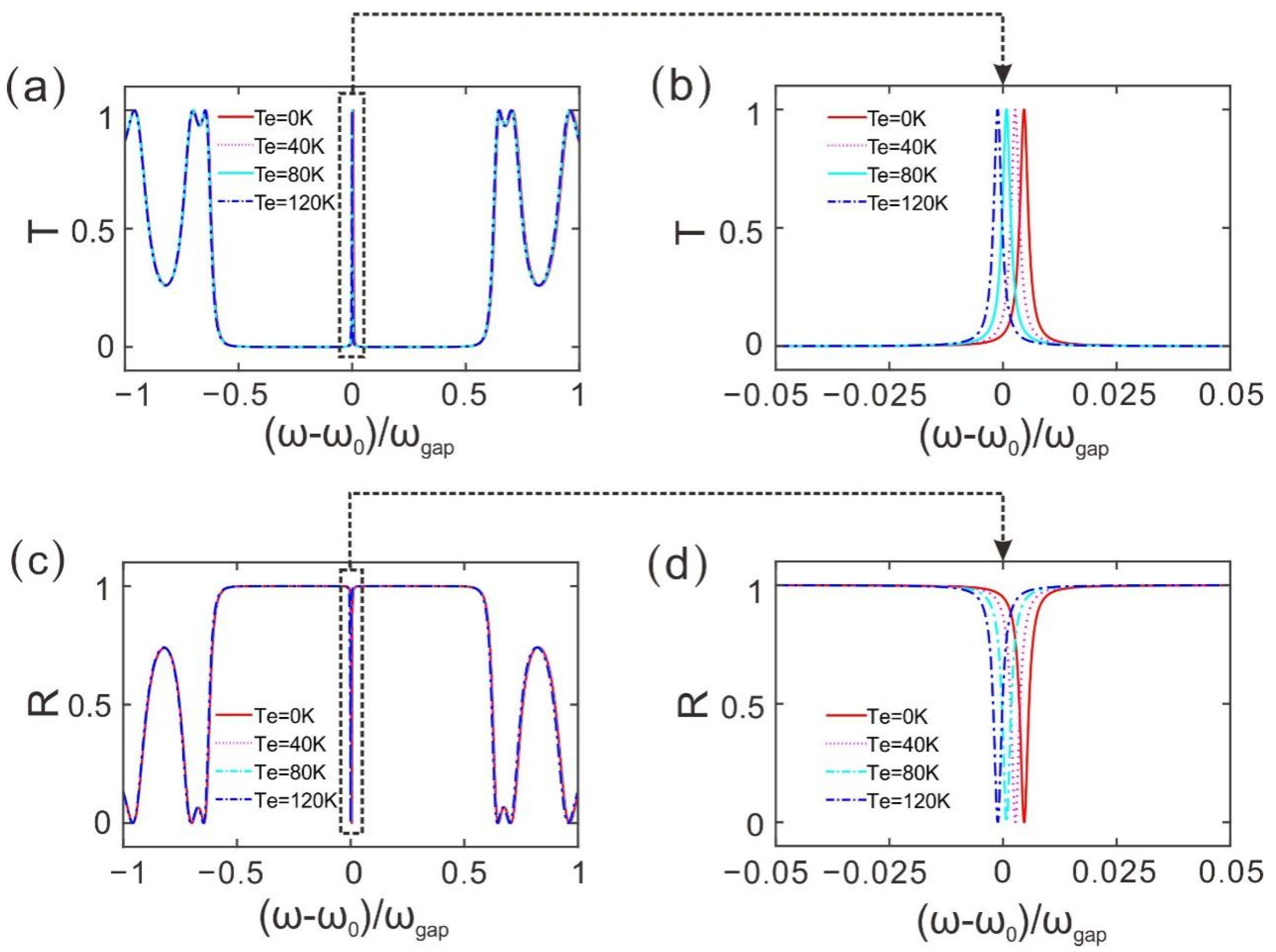
Figure 2a manifests the transmission spectrum of light waves with different temperatures (
Te = 0, 40, 80, 120 K) for
N = 3 (the structure is
ABABABBABABA). The symbol
T represents the transmittance, and the expression of the horizontal coordinate (ω − ω
0)/ω
gap is called the normalized angular frequency, where
ω = 2
πc/λ,
ω0 = 2
πc/λ0 and
ωgap = 4
ω0arcsin|(
nA −
nB)/(
nA +
nB)|
2/
π are, respectively, called the angular frequency of the light, the central angular frequency, and the photonic band gap. It can be seen that different temperatures correspond to a transmission curve. The zero-points of transmittance correspond to the photonic band gap in the range of (ω − ω
0)/ω
gap = [−1, 1]. It is found that a defect mode appears within the photonic band gap, which is also a resonance mode (denoted by the dotted area). There is a peak in the center of each transmittance curve. It is also observed that some concave bands with transmittance less than 1 appear at the edge of the band gap.
Figure 2b represents the local magnification of the defect mode. That is, the transmission spectrum of
Te = 0, 40, 80, and 120 K are respectively close-up. It can be seen that the positions of the defective peaks are not the same for different temperatures. The entire photonic bandgap has a similarly small shift to the lower frequency regions as the temperature increases. The defect mode and the bandgap edges shift to the lower frequency regions as the temperature increases. Different defective peaks correspond to different resonance wavelengths, so the extremely low temperatures can be measured according to different resonance wavelengths.
Figure 2c demonstrates the corresponding reflectance of light waves with different temperatures (
Te = 0, 40, 80, 120 K) for
N = 3 (the structure is
ABABABBABABA). The symbol
R represents the reflectance. It can be seen that different temperatures correspond to a reflection spectrum curve. There is a valley of reflection in each curve in the range of (ω − ω
0)/ω
gap = [−1, 1], denoted by the dotted area. One can find that the maxima of transmission locates at the zero points of reflectance. It is also observed that some convex bands with reflection less than 1 appear at the edge of the reflection valley.
Figure 2d shows the enlarged view of the reflection valley with different temperatures (
Te = 0, 40, 80, 120 K) for
N = 3. It can be seen that the entire reflection spectrum has a similarly small shift to the lower frequency regions as the temperature increases and the central positions of the reflection valley are not the same for different temperatures. The reflection valley also shifts to the lower frequency regions as the temperature increases.
The period number of the photonic crystal is changed when other parameters remain unchanged.
Figure 3a manifests the transmission spectrum with different temperatures (
Te = 0, 40, 80, 120 K) for
N = 4 (the structure is
ABABABABBABABABA). It can be seen that, compared with the case of
N = 3, the similarity is that different temperatures correspond to different transmission spectra. The difference is that the transmission peak at the center of the photonic band gap is narrower, meaning it resonates more strongly. The number of concave bands with low transmittance in the transmission spectrum increases as the number of periods increases.
Figure 3b represents the local magnification of the defect mode with different temperatures (
Te = 0, 40, 80, 120 K) for
N = 4. It can be seen that the defect mode and the bandgap edges shift to the lower frequency regions as the temperature increases. Comparing with the case of
N = 3, the resonance of the defect mode becomes stronger, but the position of the defective peak remains unchanged for the same temperature. Therefore, when the low temperature is measured by the effect of the central wavelength of the defect mode changing with temperature, the value of
N only affects the resonance intensity of the defect mode, but does not affect the response curve and sensitivity of the sensor.
Figure 3c demonstrates the corresponding reflectance of light waves with different temperatures (
Te = 0, 40, 80, 120 K) for
N = 4 (the structure is
ABABABABBABABABA). It can be seen that, compared with the case of
N = 3, the similarity is that different temperatures correspond to different reflection spectra. The difference is that the reflection valley at the center of the reflection curve is narrower. The number of convex bands with low reflection in the reflection spectrum increases as the number of periods increases.
Figure 3d shows the enlarged view of the reflection valley with different temperatures (
Te = 0, 40, 80, 120 K) for
N = 4. It can be seen that the center of the reflection valley and the edges of the reflection valley shift to the lower frequency regions when the temperature increases. Comparing with the case of
N = 3, the central position of the reflection valley remains unchanged for the same temperature, which is also not affected by the value of
N.
Here we demonstrate the electric field distribution of the defect mode with the period numbers
N = 3 and
N = 4, respectively. For the TM-polarized light beams normally incident from the left, the horizontal component of the electric field intensity of the defect mode is shown in
Figure 4a for
N = 3. The intensity of the electric field has been normalized. The horizontal direction is the direction of dielectric arrangement. The electric field intensity distribution of the defect mode is symmetrical. One can see that the electric field is mainly distributed in the middle of the structure, and most of the power in the electric field is restricted to the two two-layer structures
AB and
BA in the middle. The phenomenon manifests in that the defect mode can localize the electric field greatly. The light waves propagate in the dielectric multilayers and are reflected. The central two dielectric layers can be viewed as a defect referring to the periodic structure. The reflected power of the electric field constantly stacks to form the transmission mode, i.e., the defect mode. The localized effect of the electric field could be utilized for optical bistability and lasers.
Figure 4b gives the normalized electric field distribution of the defect mode in the photonic crystal for
N = 4. It also can be seen that the power of the electric field is limited at the center of the structure, specifically at the interfaces at the two layers of AB and BA around the center. Compared with the case for
N = 3, the distribution of the electric field of the defect mode has a similar profile. Therefore, the physical mechanisms of the transmission peak of the defect mode for different periodic numbers
N are the same. The value of
N does not radically affect the distribution of the electric field intensity. At the same time, the reflectance at the defect mode approximates to zero, which can induce abrupt changes in the reflection coefficient. Consequently, a giant lateral shift of reflected beams may be achieved around the defect mode in photonic crystal, especially in systems composed of weak optical loss.
Figure 5a,b show the variation of the central wavelength of the defect mode with the surroundings temperature when the period number is
N = 3 and
N = 4, respectively. The symbol of
λp represents the central wavelength of the defect mode. The red circle represents the central wavelength of the defect mode at different surrounding temperature values, and the blue line represents the fitted line based on the principle of least square method in modulations. It can be seen that the transmission peak of the defect mode at the same temperature corresponds to the same central wavelength for different values of the period number of photonic crystals. The central wavelengths of the defect modes
λp = 1.5445 μm, 1.5468 μm, 1.5491 μm, and 1.5513 μm are obtained, respectively, with the values of temperature
Te = 0, 40, 80, and 120 K. It can be found that the defect mode shifts toward to the longer wavelength when the environment temperature increases and the central wavelengths of the defect mode change approximately linearly with the temperature
Te variation from 0 K to 120 K. We use the least square method to linearly fit the curve of the central wavelength of the defect mode and obtain that the sensitivity coefficient is 5.68 × 10
−5 μm/K. Therefore, the structure is sensitive to the surrounding temperature variation and can be used for low temperature sensors.

 ,
, 


