3.1. Texture Characterization of Sb2Te Thin Films
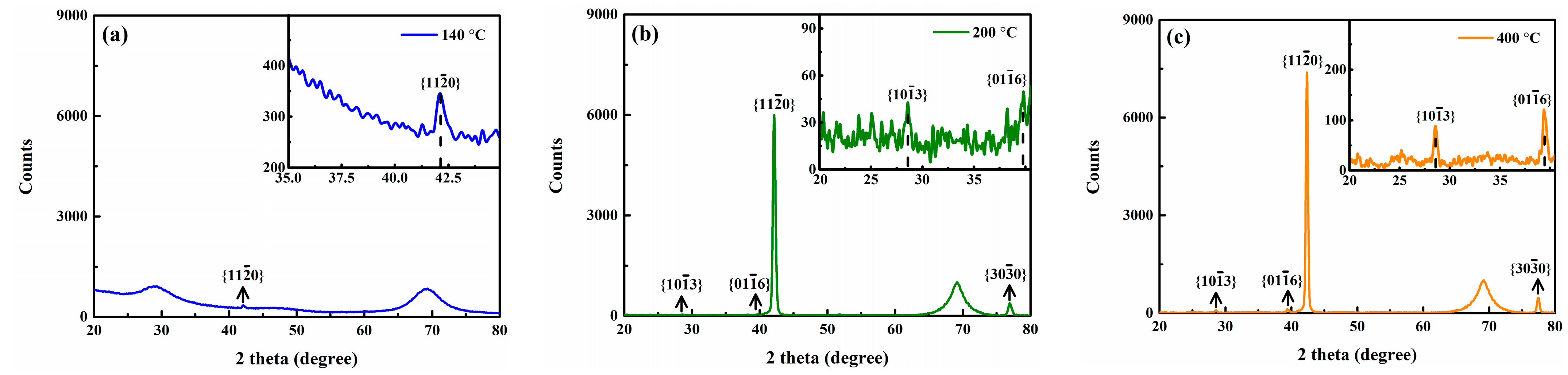
Figure 1 shows XRD patterns of Sb
2Te thin films annealed at various temperatures. After annealing at 140 °C, the amorphous diffraction peak could still be observed at ~29.2°. It suggests that the as-deposited Sb
2Te thin film is in amorphous state. Only one weak crystallographic diffraction peak appears at ~42.1°, which corresponds to the
plane of Sb
2Te thin film, as displayed in
Figure 1a. It indicates that the crystallization temperature of Sb
2Te thin film is ≥140 °C, and the Sb
2Te thin film annealed at 140 °C is not fully crystallized. A broad peak is found at ~69.3°, which is related to Si substrate, consistent with reference [
16]. As shown in
Figure 1b, when the Sb
2Te thin film is annealed at 200 °C, the amorphous diffraction peak vanishes. A sharp
diffraction peak emerges. Meanwhile, another strong peak could be observed that originates from
plane diffraction. Moreover, the weak diffraction peaks appearing at smaller angles (~28.6° and ~39.5°) are associated with
and
crystal planes. It implies that the amorphous Sb
2Te thin film is transformed into a crystalline state, and the
oriented grains exert preferential growth. As the annealing temperature increases to 400 °C (
Figure 1c), the peak intensities of
,
,
, and
planes are strengthened. It indicates the increase of crystallization fraction of Sb
2Te thin film with the increased temperature. No diffraction peaks of other phases are found in the XRD patterns, indicating the stability of Sb
2Te lattice. In addition, the
oriented diffraction peaks with higher intensity may result from the strong
texture.
Figure 2 shows the
PFs of Sb
2Te thin film measured by XRD. As displayed in
Figure 2a, when the annealing temperature is 140 °C, the maximum pole intensity of
PF is 1.2. With the enhanced annealing temperature (see
Figure 2b,c), the maximum pole intensities increase to 3.6 (200 °C) and 4.4 (400 °C), respectively. In the measured
PF, the corresponding pole sites are located near the center of the PF. When the pole density is higher than 1, distribution of pole sites deviates from randomization, indicating the existence of
orientation preference. The higher the pole density, the stronger the texture intensity. The results show that the
pole density increases with the increase of annealing temperature. That is to say, Sb
2Te thin films annealed at various temperatures possess the
texture, being compatible with the results of XRD patterns.
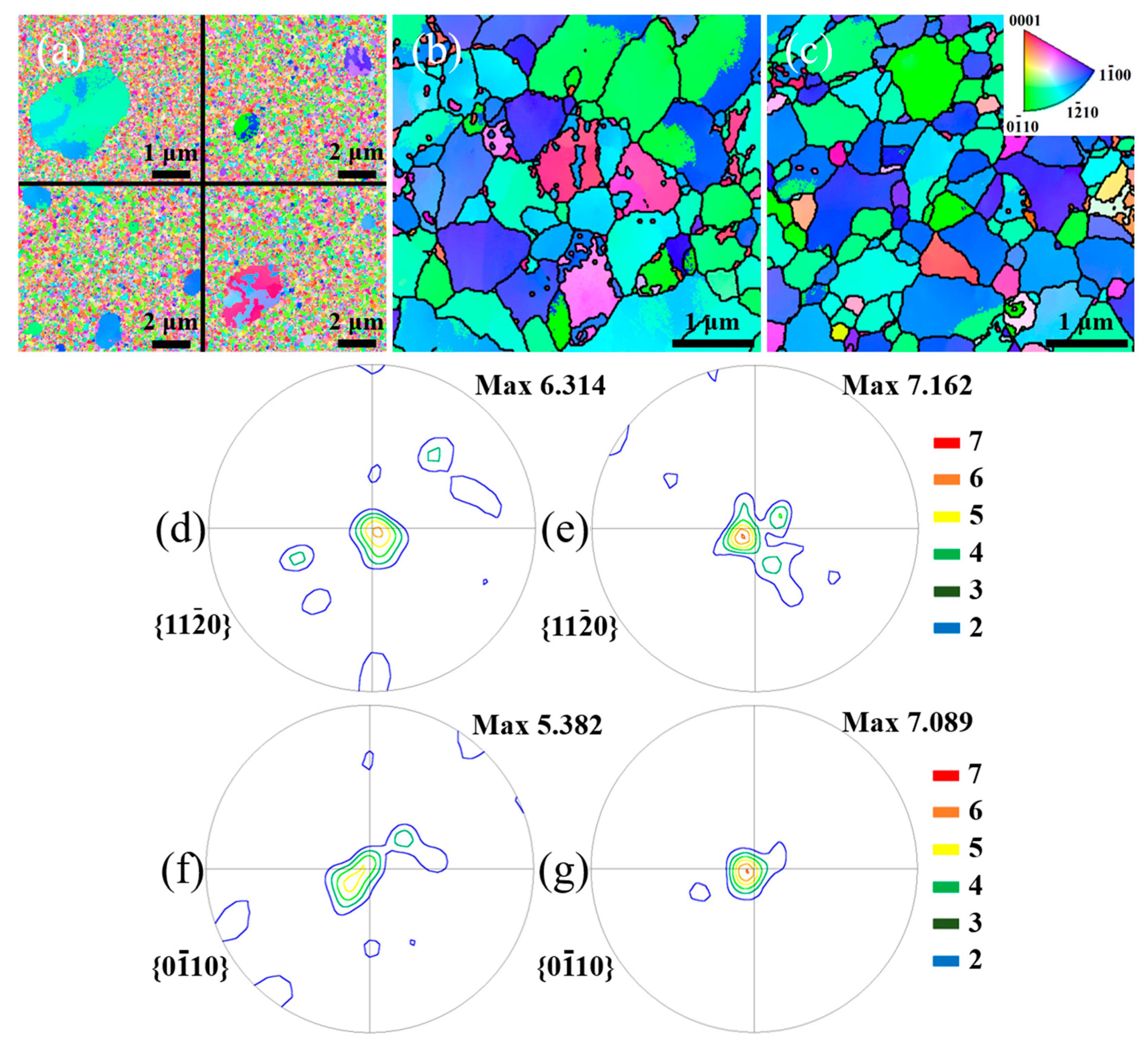
Figure 3 shows the crystallographic orientation mapping images and calculated
and
PFs of Sb
2Te thin films annealed at 140 °C, 200 °C, and 400 °C. In orientation maps (
Figure 3a–c), grains colored by red represent {0001} basal parallel to the thin film surface. The grains are marked in blue and green and possess
and
prismatic orientation. The
and
orientated grains dominate in Sb
2Te thin film, indicating the formation of a sharp prismatic texture.
Figure 3d–g show the calculated
and
PFs. Maximum pole intensities are around the center of the calculated
and
PFs, consistent with PFs measured by XRD. It indicates that the density of other orientation is weaker in Sb
2Te thin film. After annealing at 200 °C, the maximum pole densities in the
and
PFs are 6.314 and 5.382. When the annealing temperature elevates to 400 °C, maximum intensities for
and
PFs increase to 7.162 and 7.089. Therefore, the prismatic texture is formed and maintained in Sb
2Te thin film.
3.2. Formation Mechanism of Prismatic Texture
The previous results show the strong diffraction peaks of
and
planes in XRD patterns, numerous grains with
and
orientation in EBSD mappings, and high
and
pole densities in PFs. These suggest that Sb
2Te thin films exhibit
and
prismatic texture. The orientation preference may be dictated by the phase transformation, surface energy minimization, and strain energy minimization. The inheritance of texture caused by the phase transition in alloys has been confirmed [
17,
18]. Phase separation leads to inhomogeneous composition, which may be the cause of orientation preference. Phase stability of Sb
2Te thin film was considered firstly. XRD and EBSD analyses revealed the phase stability at the relative macro scale. TEM was utilized to observe the microstructure and lattice stability of Sb
2Te thin film at the microscale.
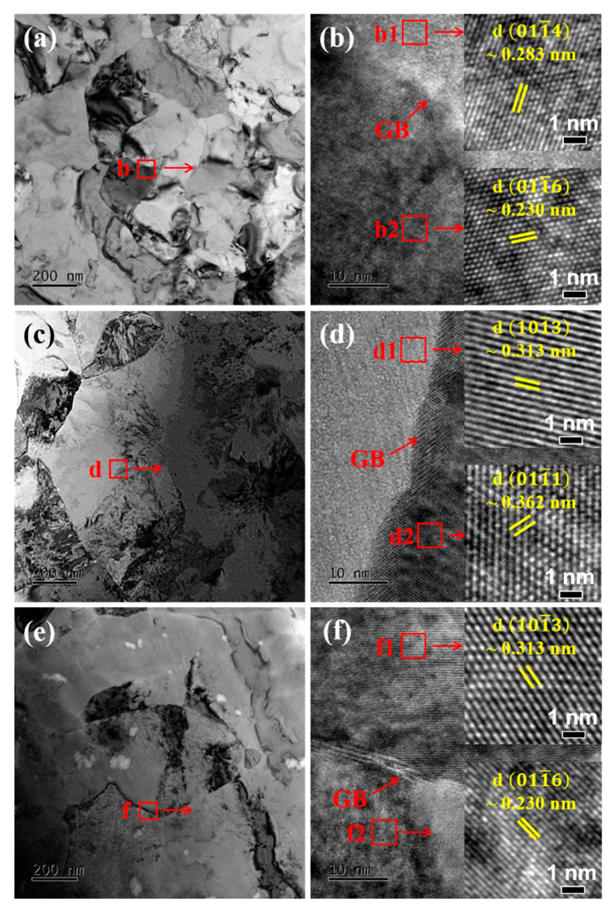
Figure 4a,c,e show the microstructure of Sb
2Te thin films annealed at 140 °C, 200 °C, and 400 °C. The second phase precipitation is not observed. We captured the high-resolution phase contrast (HRTEM) images of lattices and grain boundaries (GBs) in Sb
2Te thin film, and the inverse fast Fourier transform (IFFT) images were calculated. As shown in
Figure 4b,d,f, several crystal planes of Sb
2Te are indexed. It demonstrates the phase stability of Sb
2Te thin films at different temperatures, in agreement with the results of XRD and EBSD.
Surface energy and strain energy are essential factors driving orientation preference. The role of surface energy on the prismatic preference of Sb
2Te thin film is analyzed in this segment.
Table 1 gives the interplanar spacings of
,
,
, and
planes. For the sake of comparison, the (0001) crystal plane that exhibits the maximum interplanar spacing in Sb
2Te lattice is also provided. It knows that a larger interplanar spacing means a lower surface energy [
19]. Therefore, the surface energy of these crystal planes is arranged as follows:
>
>
>
> (0001). It has been suggested that the minimum surface energy supports (000l) orientation formation in Sb
2Te thin film [
20]. This implies that the surface energy is not the most important reason for prismatic preference.
Now we turn to the discussion of the contribution of lattice strain. The as-deposited Sb2Te thin film is in amorphous state, which has disordered atoms with a lower density, whereas annealed Sb2Te thin film is in crystalline state, in which the atoms are arranged in order. Accordingly, crystalline Sb2Te thin film has a larger atomic density and a lower volume. The rearrangement of atoms could lead to strong volume contraction in the process of crystallization. Namely, disordered–ordered phase transition results in an increase in film density, accompanied by the decreased volume. The lattice strain that is induced by volume shrinkage after crystallization is regarded as an elemental origin. The density difference results from the distinct amorphous and crystalline atomic arrangements. Consequently, a thicker Sb2Te film with a higher mass exhibits more pronounced volume shrinkage, which would promote a stronger lattice strain and prismatic preference. Therefore, we designed the thin film with two thicknesses (~200 nm and ~1000 nm) to demonstrate the contribution of the strain for the prismatic texture, and we speculated that the 1000 nm Sb2Te thin film should exhibit a stronger and prismatic texture. Annealing temperature and annealing time affect the crystallization of PCM thin film. Previous results show that the crystallization temperature of Sb2Te thin film is around 140 °C. We employed the annealing processes (170 °C: 10 min, 170 °C: 15 min, 170 °C: 25 min, and 170 °C: 35 min) to reduce the effect of crystallinity on the diffraction intensity in XRD.
Figure 5 shows XRD patterns of 200 nm and 1000 nm Sb
2Te thin films annealed at 10 min, 15 min, 25 min, and 35 min. We focus on the strong
diffraction peak that is located at ~42.2°. In 200 nm Sb
2Te thin film, the peak intensities of
planes are 3038, 6603, 6667, and 6353 when annealed at 10 min, 15 min, 25 min, and 35 min, respectively (
Figure 5a). It also occurs in 1000 nm Sb
2Te thin film, in which the peak intensities are 15,922, 30,646, 30,708, and 30,895, respectively (
Figure 5b). This indicates that Sb
2Te thin film annealed at 10 min is partially crystallized. After annealing at 15 min, both samples are fully crystallized.
Figure 6 shows XRD patterns of 200 nm and 1000 nm Sb
2Te thin films annealed at 15 min and 35 min. All Sb
2Te thin films exhibit four narrow diffraction peaks. Diffraction peaks emerge at ~28.7°, ~39.8°, ~42.2°, and ~76.9°, corresponding to
,
,
, and
planes.
Table 2 gives the diffraction peak intensities. The peak intensities of the
and
diffraction planes in the 1000 nm Sb
2Te thin film are clearly higher than those in the 200 nm thin film. It implies that 1000 nm Sb
2Te thin film has a stronger
and
preference. More importantly, the
and
peak intensities of the two films are a little different. It means that the number of crystals involved in diffraction has a relatively weak effect on peak intensity. That is to say, the impact of film thickness on the diffraction strength is weak in the present result. Therefore, the degree of prismatic preference in 200 nm and 1000 nm Sb
2Te thin films could be discussed by using reasonable annealing processes (170 °C: 15 min and 170 °C: 35 min).
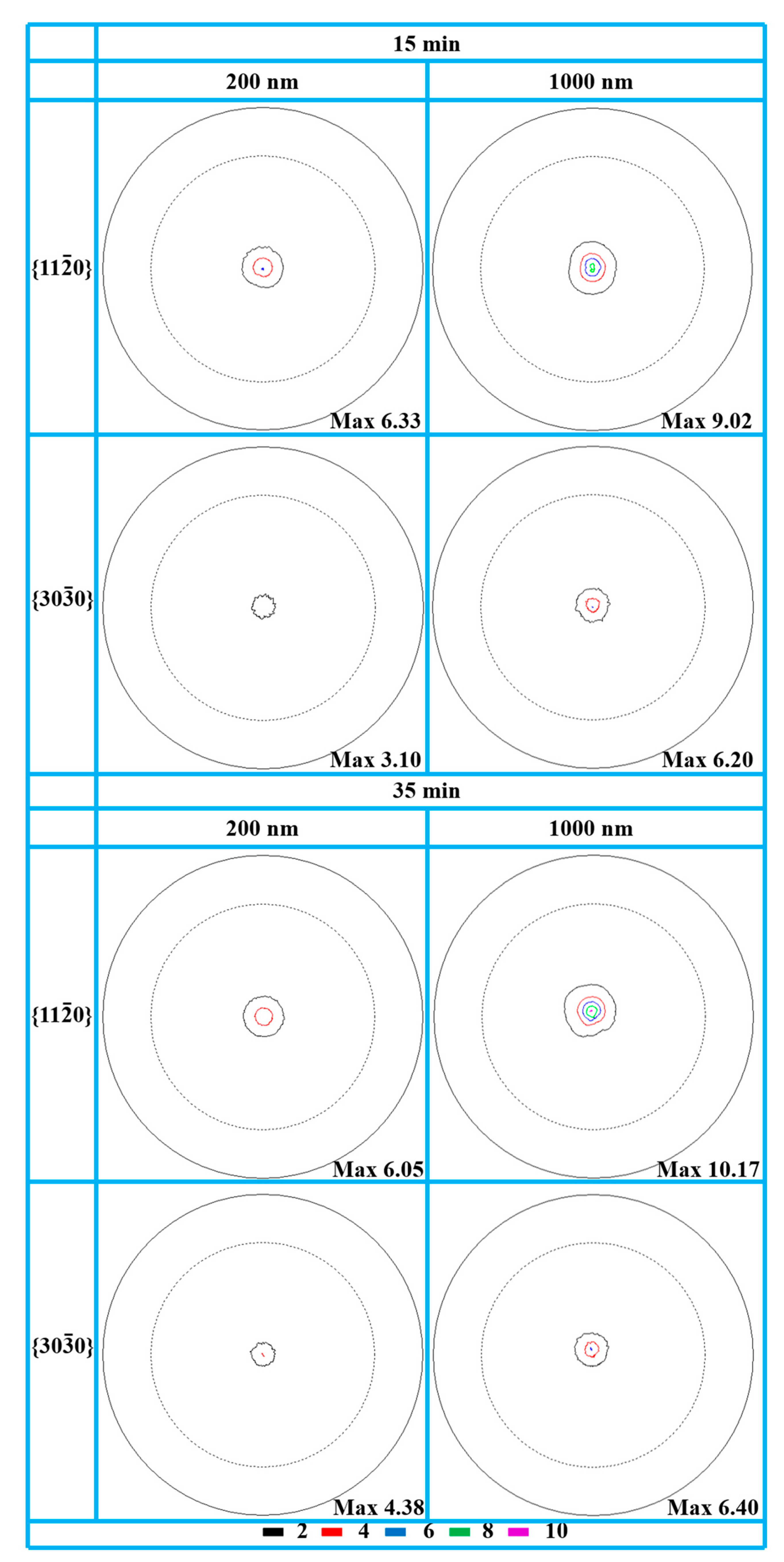
Figure 7 shows the measured
and
PFs of 200 nm and 1000 nm Sb
2Te thin films annealed at 15 min and 35 min. As displayed in the top panel, after annealing for 15 min, the maximum intensity of
PF is 9.02 for 1000 nm Sb
2Te thin film, higher than that in 200 nm Sb
2Te thin film (6.33). Simultaneously, in the 1000 nm Sb
2Te thin film, the maximum intensity of
PF is 6.20, which is twice that of the 200 nm Sb
2Te thin film (3.10). Moreover, maximum densities of
and
PFs are not significantly affected by the prolonged annealing time, as illustrated in the bottom panel. Therefore, 1000 nm (thicker) Sb
2Te thin film exhibits a stronger prismatic texture, consistent with XRD patterns and our predictions.
Mitra et al. [
22] reported that the strain caused by the density difference between crystalline and amorphous states leads to the structural variations of the amorphous phase. It means that the minimization of the strain energy may provide driving force to deform the lattice. Mechanical analysis of a Sb
2Te unit cell offers insight into the strain-driven prismatic texture formation. The anisotropic modulus quantitatively describes the deformation resistance in various crystallographic orientation. Unfortunately, to the best of our knowledge, no experimental information on the anisotropic modulus of the Sb
2Te crystal was available to discuss. The anisotropic modulus originates from the bonding strength in different directions in the lattice. The stronger the bonding in a certain orientation, the greater the anisotropic modulus. The space group of Sb
2Te is P −3 m 1. The Sb
2Te lattice comprises octahedral Sb
2Te
3 and Sb
2Sb
2 structural primitives, which are stacked layer by layer along the c-axis. The atomic layers are bonded by van der Waals (vdW) bonds. Therefore, bonds in the prismatic orientation are weaker than in others, leading to a stronger tendency to deform. As found by Raoux et al. [
23], the Sb
2Te lattice expands along the <0001> axis with the increased annealing temperature. It implies that the prismatic direction more easily deforms.
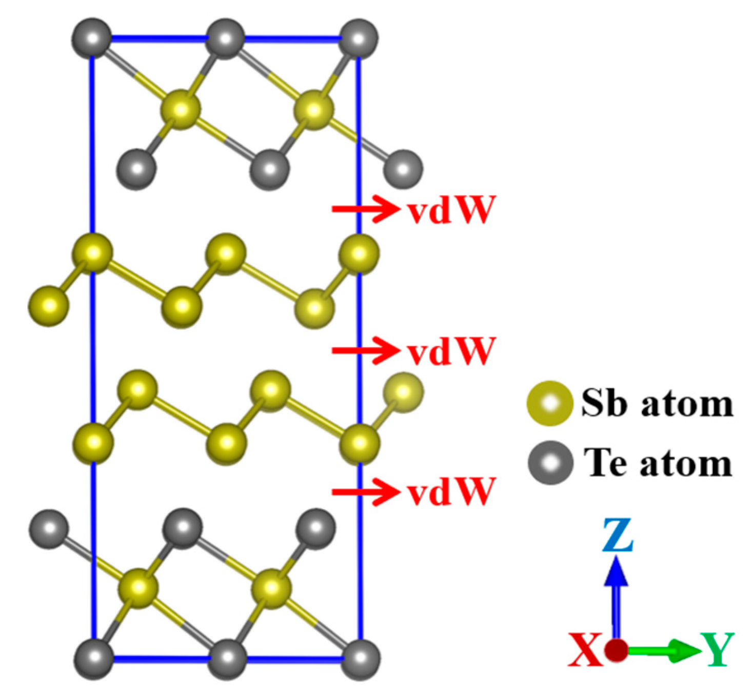
Figure 8 shows the schematic diagram of Sb
2Te lattice, where the weak van der Waals bonds are located between the Sb–Sb and Sb–Te atomic layers.
Table 3 gives the structural parameters of 200 nm and 1000 nm Sb
2Te thin films. After annealing for 15 min, the diffraction angles of
(2
θ = 42.054°) and
(2
θ = 76.757°) in the 1000 nm Sb
2Te thin film are lower than those in the 200 nm Sb
2Te thin film (42.170° for
and 77.010° for
). Consequently, a larger lattice parameter (
a) is shown for 1000 nm Sb
2Te thin film. Similar results are displayed for Sb
2Te thin film annealed at 35 min. The value of (
a) measured by using power XRD is 0.4272 nm for single-crystal Sb
2Te [
21], which is relatively close to the value of 200 nm Sb
2Te thin film (~0.4280 nm) and is clearly smaller than that of 1000 nm Sb
2Te thin film (~0.4290 nm). This could also infer that the degree of lattice distortion is higher in the 1000 nm Sb
2Te thin film. The lattice parameter (
c) was not calculated because the diffraction signals of
and
planes are weak. In 1000 nm Sb
2Te thin film, a stronger volume shrinkage in the crystallization process induces a greater lattice strain. The c-axis with weaker bonding appears to be compressed. The a-axis is extended to maintain the stability of Sb
2Te lattice. Consequently, the 1000 nm Sb
2Te thin film exhibits a larger lattice parameter (
a). This may be an acceptable explanation. Zhou et al. [
20] suggested that Sb
2Te lattice with compressed c-axis is more stable because of the restricted atom free space. Therefore, the lattice strain is an important factor for the prismatic preference, and the prismatic texture could be maintained in Sb
2Te thin film. Note that differing surface energy may be the reason for the difference in the strength of
and
orientation. In addition, Sb
2Te thin film has coarser grains due to the grain-growth-dominated crystallization, which is not conducive to freeing the stress. Therefore, the prismatic texture of single-phase Sb
2Te thin film is caused by the lattice strain, surface energy of the crystal plane, and coarse grain, where the lattice strain is a major contributor.
3.3. Electrical Properties of Prismatic Textured Sb2Te Thin Film
We investigated the electrical properties of prismatic textured Sb
2Te thin film by using PPMS. Sb
2Te thin film exhibits
p-type conductivity, which is consistent with other Sb-rich PCM thin films [
24,
25]. It suggests that the excited holes dominate the electrical transport in Sb
2Te thin film, originating from the structural vacancies. In Sb–Te binary alloys, Sb vacancies and Sb
Te antisite defects are confirmed to be the essential carriers [
26].
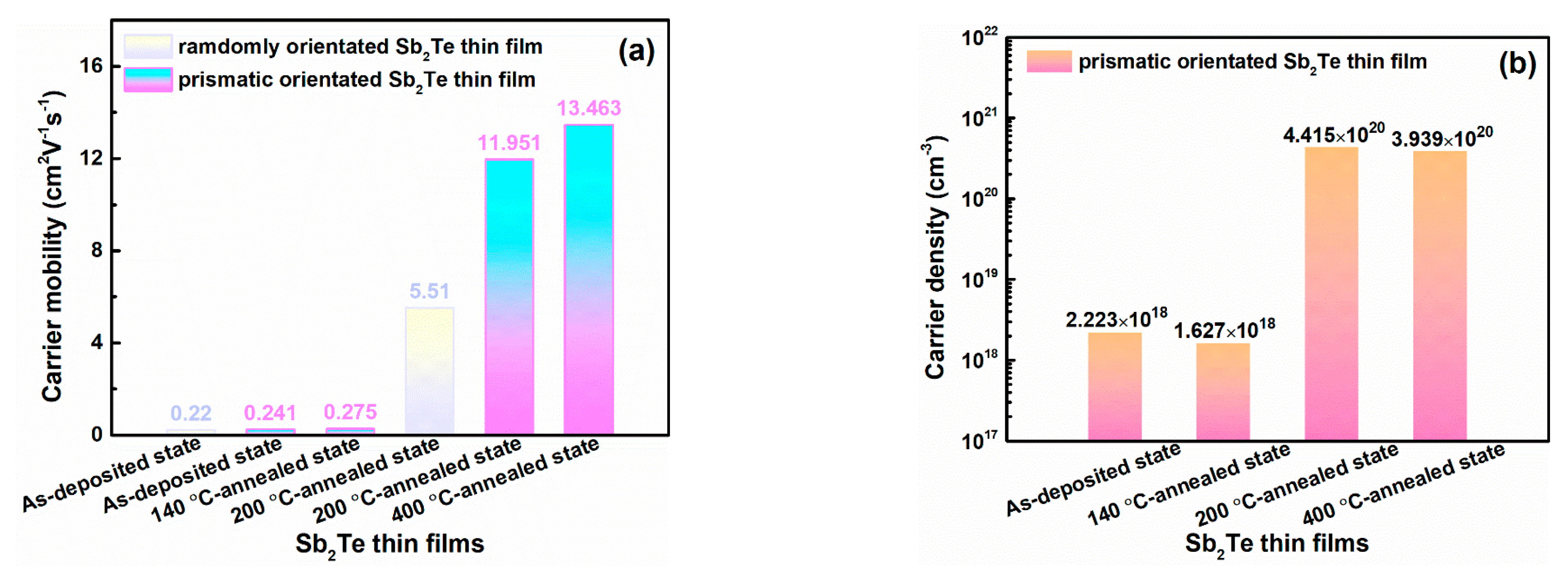
Figure 9a shows the carrier mobility of as-deposited (amorphous) and annealed (crystalline) Sb
2Te thin films. Carrier mobility of as-deposited Sb
2Te thin film is 0.241 cm
2V
−1s
−1, almost equal to the result (0.220 cm
2V
−1s
−1) [
27]. In amorphous thin film, carrier mobility strongly depends on the localized state, which is related to the degree of structural disorder [
28]. When the annealing temperature is 140 °C, carrier mobility is maintained, which results from the weak crystallinity, as shown in XRD and EBSD. Therefore, carrier mobility may be susceptible to the atomic arrangement. In fully crystallized Sb
2Te thin film, carrier exhibits a higher mobility. We compared the carrier mobility of 200 °C annealed Sb
2Te thin films with prismatic texture and with random orientation. It is obvious that textured Sb
2Te thin films have higher carrier mobility, as displayed in
Figure 9a. We have reasons to suppose that prismatic texture promotes carrier migration. Texture formation improves the alignment and connectivity of grains in the thin film, which helps to increase the average free path of the carrier [
29]. PCM thin film with fiber texture possesses more coincidence boundaries [
30]. Grain boundary potential barrier is related to the misorientation of grains. As measured by Tsurekawa et al. [
31], the potential barrier height of coincidence boundaries is lower than twice that of random boundaries. Therefore, in prismatic orientated Sb
2Te thin film, the carrier could encounter less grain scattering and trapping. It thus increases the mean free path and mobility of the carrier. As shown in
Figure 9a, Sb
2Te thin film annealed at 400 °C exhibits a stronger prismatic texture and carrier mobility. The impact of grain growth on the carrier transport should not be overlooked. It is stressed that grain with preferred orientation has greater growth advantage, which further reduces the grain boundary scattering effect. Therefore, there are two points in addressing the role of prismatic texture on carrier mobility in Sb
2Te thin film. On the one hand, prismatic texture improves the degree of atomic ordering and decreases the grain boundary potential barrier to enhance carrier transfer. On the other hand, grain with prismatic preferred orientation is further coarsened to facilitate carrier mobility.
Figure 9b shows the carrier density of as-deposited and annealed Sb
2Te thin films with prismatic texture. At higher annealing temperature (400 °C), Sb
2Te thin film exhibits lower carrier density (3.939 × 10
20 cm
−3) than that annealed at 200 °C (4.415 × 10
20 cm
−3). It implies that the vacancy density decreases at higher temperature. To our knowledge, texture formation may reduce the structural defects at the grain boundary. Nevertheless, dependence of carrier density on the texture needs to be addressed. From the viewpoint of carrier mobility, reducing the intensity of prismatic texture could inhibit carrier transport, thus improving the resistance of Sb
2Te thin film to decline power consumption.


