Article

Vapor Deposition Growth of SiC Crystal on 4H-SiC Substrate by Molecular Dynamics Simulation

1
School of Power and Mechanical Engineering, Wuhan University, Wuhan 430072, China
2
School of Computer Science, Wuhan University, Wuhan 430072, China
3
The Institute of Technological Sciences, Wuhan University, Wuhan 430072, China
*
Authors to whom correspondence should be addressed.
Crystals 2023, 13(5), 715; https://doi.org/10.3390/cryst13050715
Submission received: 16 March 2023 / Revised: 10 April 2023 / Accepted: 17 April 2023 / Published: 23 April 2023
(This article belongs to the Section Industrial Crystallization)

Abstract

:
Due to the lack of appropriate experimental methods for imaging the evolution of the microstructure of materials at the growth conditions, our understanding of the physical behavior of crystal growth and defect formation during the vapor deposition growth of SiC crystals is still rather limited. In the present work, the vapor deposition growth of SiC crystal on a 4H-SiC substrate has been investigated by the molecular dynamics (MD) computer simulation method. Three different lattice planes of 4H-SiC ( ( 0001 ) , ( 11 2 - 0 ) and ( 1 - 100 ) ) were selected as the surface of the substrate, and three different temperatures for substrate (2200 K, 2300 K and 2400 K) were used in growth simulations. The characteristics of the formation of different polytypes of SiC and dislocations in the grown crystals were examined. The results show that the SiC crystals were grown by a subsurface nucleation and growth mode in the vapor deposition process. For substrates with ( 0001 ) plane as the surface, the 3C-SiC single crystal was obtained in the deposited thin film. For substrates with ( 11 2 - 0 ) or ( 1 - 100 ) plane as the surface, the 4H-SiC single crystal was obtained instead. The temperature of the substrate was found to have a significant effect on the dislocation density generated in the grown crystals. The mechanism for the formation of Frank partial dislocations during the growth of SiC crystals has been analyzed, for which the importance of the diffusivity of atoms on the surface layer in growth has been highlighted, and it gives a good explanation of the temperature effect on dislocation formation in the grown crystals. These results can be helpful for experimental vapor deposition growth of SiC single crystals and epitaxial layers of high quality.

1. Introduction

With the rapid development of power management-related engineering applications such as electric vehicles and smart grids, power semiconductor devices are now receiving more and more attention. In these power electronics application scenarios, materials and devices are required to withstand large switching voltages, high switching frequencies and long operation times without failure. For this purpose, traditional semiconductors such as silicon materials are considered inadequate for improved advanced applications. As a wide band gap semiconductor material, silicon carbide, especially the 4H-SiC, is widely recognized to be a better choice due to its excellent physical and chemical properties, such as high breakdown voltage, high electron mobility, high thermal conductivity and excellent chemical resistance. It is now generally considered the optimum solution for next-generation power electronic devices and is much favored in industry practice [1].
Since there is no liquid phase of SiC with stoichiometric concentration under easily achievable process conditions, both the single crystal boules and epitaxial wafers of SiC for power electronic devices are generally grown and prepared by vapor deposition methods. For example, the physical vapor transportation (PVT) method or high-temperature chemical vapor deposition (CVD) method is currently used to obtain single crystals of SiC with a certain size on the SiC seed crystals [2]. For epitaxial wafers, the CVD method is generally used to obtain an epitaxial thin film layer with specific thickness and dopants concentrations on the sliced and polished SiC wafer substrate [3,4]. So far, 4H-SiC boules grown by the PVT method with a diameter of 150 mm have been commercially available, and SiC wafers with a diameter of 200 mm have been reported to be successfully grown and prepared [5,6]. During the vapor deposition growth process, a number of defects, including the various polytypes of SiC, various kinds of dislocations and stacking faults, can be generated in the SiC crystals obtained, depending on a number of thermodynamic factors, such as temperature field and vapor pressure in the chamber. The presence of these defects often has a considerable adverse effect on the performance or is even fatal for the usage of power electronic devices.
Take polytypes as an example. There are more than 200 SiC polytypes known to exist in nature [7]. They can be characterized by their unique stacking sequences of the closest packed Si-C diatomic layers (i.e., {111} of the cubic lattice and {0001} of the hexagonal lattice) along the direction perpendicular to this closest packed plane [8]. The ideal 3C-SiC structure has a stacking order of ABCABC… along the <111> direction, and the ideal 4H-SiC structure has a stacking order of ABCBABCB… along the <0001> direction, where A, B and C represent the three different candidate stacking positions of the closest packed Si-C diatomic layer when stacking it on the other closest packed Si-C diatomic layer. During the vapor deposition growth of SiC, different polytypes may be formed and mixed with each other, bringing adverse effects to the performance of power devices. It has been shown that the temperature of the substrate or seed crystal has a direct effect on the selection of polytypes during vapor deposition growth [9,10]. For example, 3C-SiC tends to form at lower temperatures and 4H-SiC at higher temperatures [11]. In addition, the growth rate and the surface characteristics of the seed crystal or substrate are also important factors that determine whether a certain polytype forms or not during growth [1,12].
The reduction of dislocation density in the SiC crystal grown is also a major concern for the vapor deposition growth and preparation of high-quality SiC boules and epitaxial wafers. It is generally believed that stress-induced plastic deformation is one of the main reasons for the formation of dislocations within the material. Therefore, the thermal stresses in the substrate and epitaxial film or in the boule during growth, especially the distribution of shear stress components in the crystal, should play a key role in the generation of dislocations in SiC crystals [13]. When the stress along the main slip system exceeds the critical stress for activation of the dislocation source (about 1 MPa at 2200–2300 °C [14,15]), slip and dislocation multiplication will occur, resulting in an increase in dislocation density in the crystal. The thermal stress can be introduced by different levels of thermal expansion in different areas of the SiC crystal due to the radial or axial temperature inhomogeneities in the SiC crystal [16]. In addition, dislocations in the surface layer of the substrate will also be inherited and extended into the grown crystal during the epitaxial growth process [17]. Therefore, it is also very important for the preparation of SiC boules with lower dislocation densities in order to obtain epitaxial wafers with reduced dislocation densities.
Due to the very high temperature (1500–2300 °C) required for vapor deposition growth of both SiC boule and epitaxial wafer, and also because of the limitation of experimental methods (e.g., there is a lack of in situ high-resolution microscopy for imaging the evolution of microstructure of materials at such growth conditions), our understanding of the thermodynamic behavior and underlying mechanisms of crystal growth and defect formation and their relationship with the processing conditions during the vapor deposition growth of SiC crystals is still rather limited [18,19]. The molecular dynamics (MD) method, which is an atomic-scale computational materials simulation technique, can give accurate details of the atomic-scale time evolution of the material during the growth process. It can serve as an alternative and valuable way to help analyze the physical and chemical behavior of crystal growth and defect formation during the vapor deposition growth of SiC crystals [18,20].
In the present work, we investigated the vapor deposition growth of SiC crystals on 4H-SiC substrates (or seed crystals) using the computer MD simulation method. Different lattice planes, including basal plane ( 0001 ) , non-basal planes ( 11 2 - 0 ) and ( 1 - 100 ) were selected as the surface of the 4H-SiC substrates, and different substrate temperatures (2200 K, 2300 K and 2400 K) were used for MD simulation of vapor deposition growth of the SiC crystal. The effects of different substrate surfaces and substrate temperatures on the formation of polytypes, dislocation density and dislocation characteristics of the grown crystals were examined. The underlying mechanisms for the formation of Frank partial dislocations during the vapor deposition growth of SiC crystals have been analyzed as well. A brief discussion of all the results is given at the end.

2. Method

2.1. Interatomic Potential of the Atomistic Models

Several interatomic potential functions have been developed up to now for Si-C binary systems, including Vashishta [21], Tersoff [22], environment-dependent interatomic potential (EDIP) [23] and the modified embedded atom method (MEAM) [20]. Although these potential functions have been shown to give a good description of a range of physical properties of SiC materials, such as mechanical properties, crystal defect structure and irradiation behavior, it is, however, unclear whether they can reasonably describe the vapor deposition growth process of SiC crystals. To clarify, we have performed some preliminary tests and checked these interatomic potential functions by MD simulation of the high-temperature vapor phase epitaxial growth of SiC using these different potential functions. It was found that the structure of epitaxial films given by the test simulations are all disordered at a range of thermodynamic conditions when the Vashishta, Tersoff and EDIP potentials were used, while the test simulations using the MEAM potential can give SiC crystals within a certain temperature range. Therefore, the MEAM potential was selected for the computational MD simulation of vapor deposition growth of SiC crystals in the following study.

2.2. Atomistic Models and Simulation Procedure

All the MD simulations in this work were performed by using the LAMMPS [24] code. Figure 1 shows the three atomistic models constructed for the 4H-SiC substrate with different crystal lattice planes as the substrate surface, i.e., ( 0001 ) plane in Figure 1a, ( 11 2 - 0 ) plane in Figure 1b, and ( 1 - 100 ) plane in Figure 1c. The sizes of the models for the substrates in Figure 1a–c are 213 Å × 209 Å × 20 Å, 138 Å × 152 Å × 22 Å and 150 Å × 151 Å × 18 Å, respectively. Periodic boundary conditions were used in the X- and Y- directions of the models, and a free surface boundary condition was applied in the Z- direction with a vacuum region of fixed size above the surface of substrates to facilitate the insertion and deposition of Si and C atoms to the surface of the substrates.
For the initially constructed models of substrates, an optimization of the positions of atoms and the dimensions of the models was first performed by using the conjugate gradient energy minimization method combined with the relaxation of the models at zero stress using the Parrinello–Rahman method for stress control [25]. Initialization of the velocities of all the atoms in the models of the substrates was then given according to the target temperatures of the substrates to be controlled in vapor deposition processes. In the subsequent MD simulations, the temperature of the substrates and the overall size of the models (including the vacuum space) were kept fixed. Three different temperatures for the substrates were adopted in the vapor deposition growth of SiC thin films, i.e., 2200 K, 2300 K and 2400 K. A border zone consisting of a layer about 3 Å in thickness at the bottom of the models of the substrates was designed. The atoms in this border zone remain frozen during the vapor deposition growth simulation to prevent the substrates from moving due to the impingement of atoms deposited on surface of the substrates, while the other atoms in the substrate are free to move according to the Nose–Hoover equation of dynamics [26,27,28] at the desired temperature of the substrate.
The vapor deposition growth of SiC crystals was simulated by insertion of a total number of 60,000 Si atoms and 60,000 C atoms (C/Si ratio equal to 1) at randomly selected points on the cross-section of the vacuum space at a height of about 218 Å above the surface of substrate and with a constant rate of insertion for each of the models. The direction of incidence of the inserted atoms is perpendicular to the substrate surface and downward, as shown in Figure 1. The total time duration of the deposition process is 30 ns. All the atoms, thus inserted, move following the Newtonian dynamics in the process of deposition. After the finish of deposition process, MD simulation of the whole system was kept run for another 2 ns without change of the settings of the dynamics to give thermal equilibration of the thin film deposited. The initial velocity of each atom inserted is vz, which satisfies the following relation [20]
v z = 2 K i M i
where Ki = 1/2κBTE represents the kinetic energy of the inserted atom calculated by one-third of the thermal energy of an atom in evaporation source with the temperature of TE, κB is the Boltzmann constant, and Mi represents the mass of the inserted atom. Here, we set the temperature (TE) of the evaporation source to be 300 K higher than that of the substrate, which is roughly comparable to the setting adopted in the usual vapor deposition growth experiments correspondingly [1].

2.3. Methods for Characterization of Crystal Structure and Defects

We used the open-source visualization tool OVITO [29] to analyze the simulation results and to image the crystal structure, surface topography and dislocations of the atomistic models. The characteristics of stacking and local arrangement of the atoms in the models were analyzed using the “identify diamond structure (IDS)” method [30], which is based on a modified common neighbor analysis (CNA) technique and is incorporated in OVITO. By analyzing the topologies and coordination structure of all the atoms within the nearest and second nearest neighbor shells of each atom, the characteristics of stacking and local arrangement of each atom can be analyzed and classified into seven categories [29,30]: “Cubic diamond”, “Cubic diamond (1st neighbor)”, “Cubic diamond (2nd neighbor)”, “Hexagonal diamond”, “Hexagonal diamond (1st neighbor)”, “Hexagonal diamond (2nd neighbor)” and “Other”. Based on this classification, atoms with a local hexagonal lattice arrangement (i.e., wurtzite structure, denoted as “wz”) or a local cubic lattice arrangement (i.e., zinc blende structure, denoted as “zb”) in SiC crystals can be identified in the atomistic models, and the possible existence and distribution of the various polymorphic structures of SiC crystals as well as the lattice defects within the models can be recognized.
In addition, the method of dislocation extraction algorithm (DXA) [31] included in the OVITO software was used to analyze and identify the dislocation lines and their Burgers vectors in the atomistic models. The DXA method can well identify dislocations in various kinds of lattices and grain boundaries, including partial dislocations and secondary dislocations at grain boundaries. It has been widely used in various atomic-scale computational simulations of materials [32,33,34].

3. Results

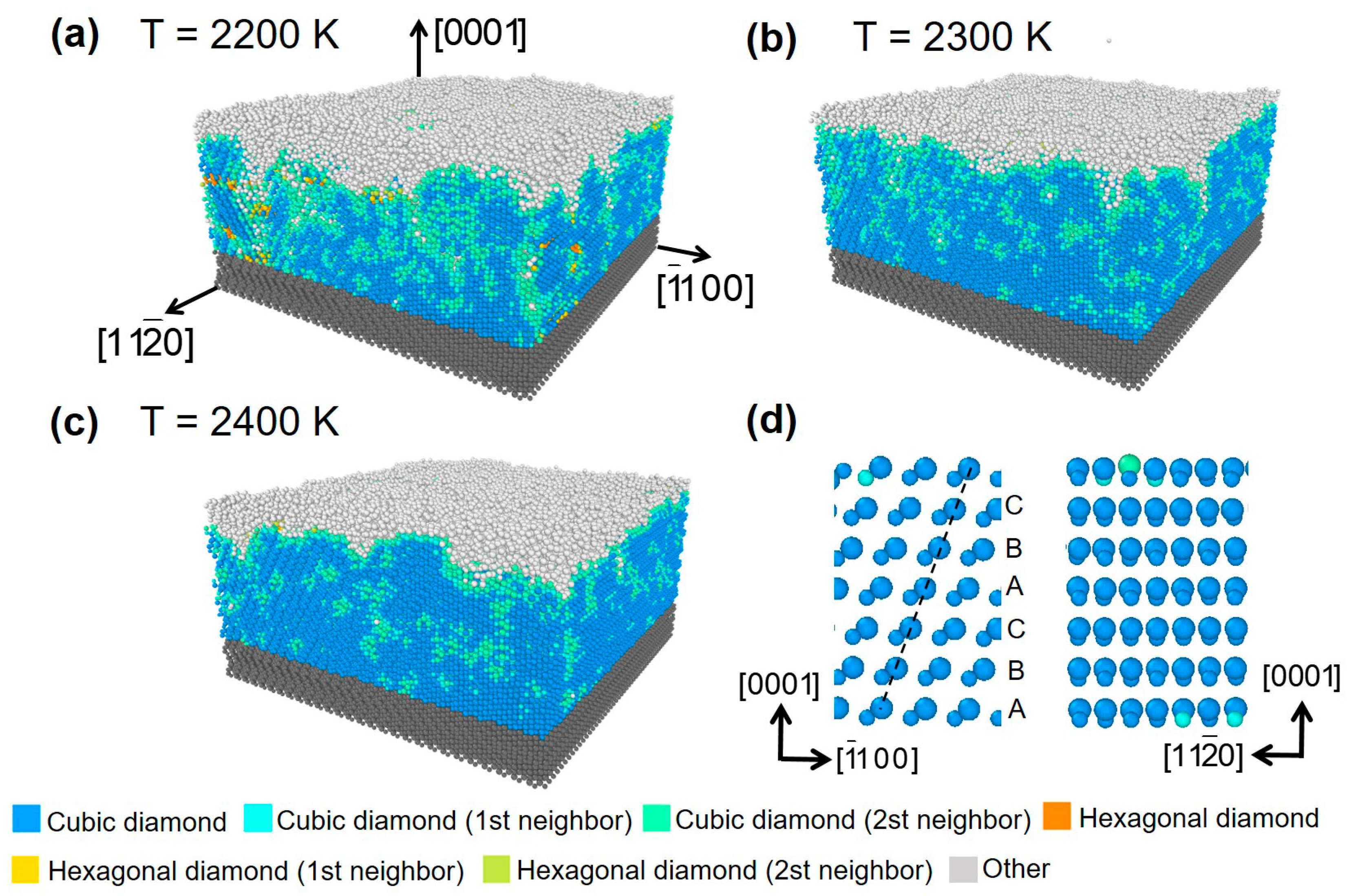
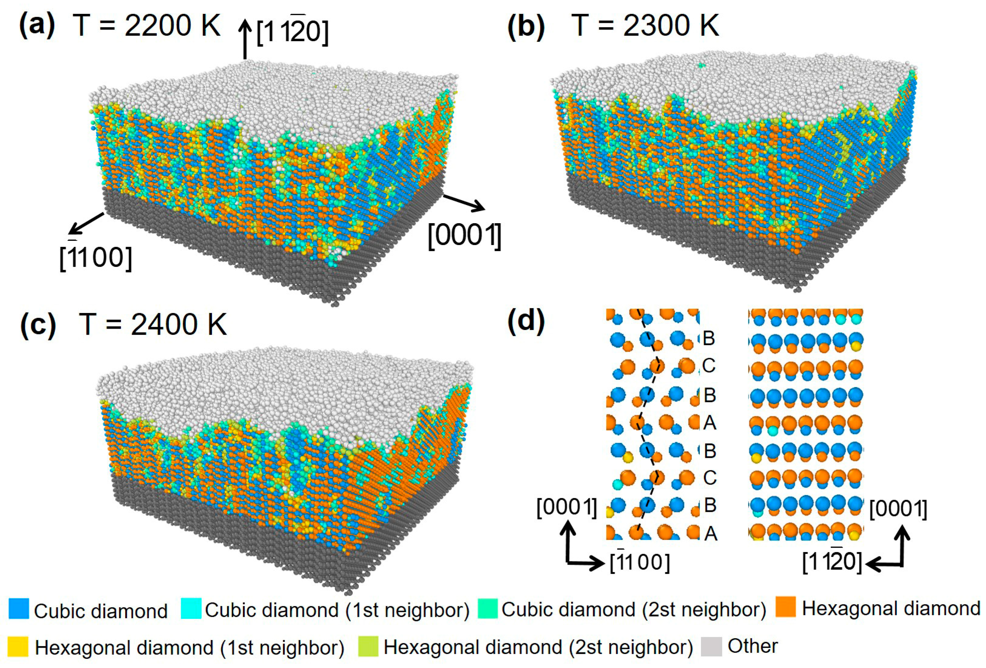
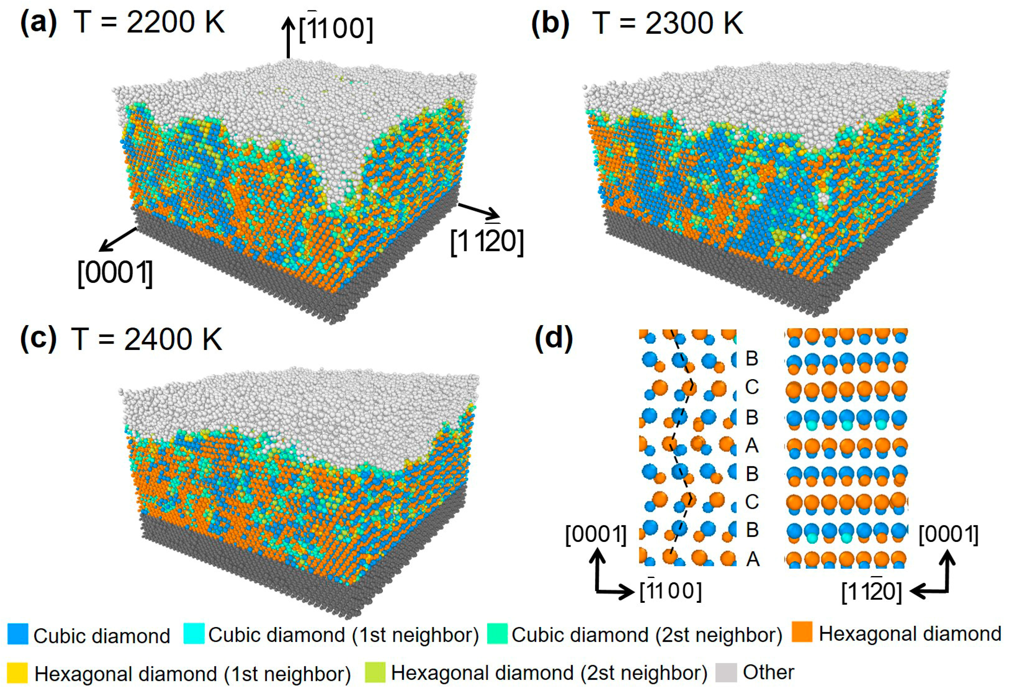
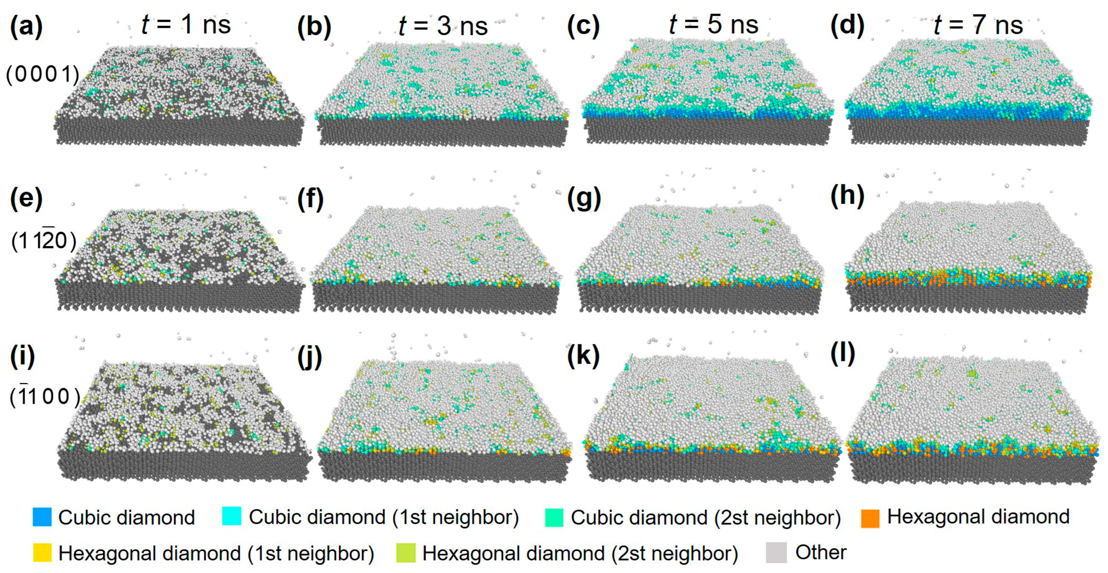
3.1. The Atomistic Structure and Polytypes of SiC Formed in the Deposited Films

The atomistic structure of the SiC thin films deposited on the 4H-SiC substrates with the ( 0001 ) Si-terminated plane as the surface is shown in Figure 2. As can be seen in Figure 2a–c, for all the three selected temperatures of substrate of 2200 K, 2300 K and 2400 K, there is an amorphous layer of about 1–3 nm thick on top of the surface of the thin film deposited, while the atoms in the thin film below the amorphous layer are mostly characterized by the cubic diamond structures according to the analysis using the IDS method. A detailed analysis of the arrangement of atoms in the region below the surface amorphous layer reveals that a stacking order of ABCABC… of the closest packed Si-C bilayer in this region can be recognized, as shown in Figure 2d, which is consistent with the stacking order of the ideal 3C-SiC crystal. Therefore, it can be determined that the atoms in the thin film beneath the surface amorphous layer form a 3C-SiC crystal for vapor deposition growth at all three selected temperatures of the substrate. This is in agreement with the previous experimental report that 3C-SiC single crystal films were obtained by epitaxial growth on the 4H-SiC ( 0001 ) Si-terminated surface [35]. In addition, Figure 2a–c also show that there is a small fraction of atoms of other structural features in the crystals formed on deposition, which are presumed to be various kinds of crystal defects in the grown 3C-SiC crystals, such as point defects and dislocations. It is also worth mentioning that we have performed similar MD simulations of vapor deposition growth processes on a 4H-SiC substrate with the ( 0001 ) C-terminated plane as the surface, and it shows that the crystals in the thin films obtained are also 3C-SiC.
Figure 3 shows the atomistic structure of the SiC thin films deposited on the 4H-SiC substrate with the ( 11 2 - 0 ) plane as the surface. As can be seen in Figure 3a–c, the thin films deposited on the ( 11 2 - 0 ) plane of 4H-SiC at temperatures of substrate of 2200 K, 2300 K and 2400 K also have an amorphous layer about 1–3 nm thick on top of the surface. However, the local arrangement of atoms below the amorphous layer is characterized by an ordered mixture of cubic diamond and hexagonal diamond structures according to the analysis using the IDS method, indicating that a different polytype of SiC crystal has been formed. From Figure 3d, it can be seen that a stacking of the closest packed Si-C bilayers with the order of ABCBABCB… can be identified in this crystalline region, which is consistent with the stacking structure of an ideal 4H-SiC crystal. It can also be found that the ratio of the number of atoms in the cubic diamond structure and that of the hexagonal diamond structure is close to 1:1, which conforms to the properties of an ideal 4H-SiC crystal with 1/2 hexagonality. Therefore, it can be determined that the atoms in the thin film beneath the surface amorphous layer form a 4H-SiC crystal for vapor deposition growth in these cases.
Figure 4 shows the atomistic structure of the SiC thin films deposited on the 4H-SiC substrate with the ( 1 - 100 ) plane as the surface. It can be seen from Figure 4a–c that the atomistic structures of the thin films deposited and grown on the ( 1 - 100 ) plane of 4H-SiC at temperatures of substrate of 2200 K, 2300 K and 2400 K bear close resemblance to those of the thin films grown on the ( 11 2 - 0 ) plane, as shown in Figure 3, which is characterized by the same mixed structure of cubic diamond structure and hexagonal diamond structure beneath a surface amorphous layer according to the analysis using the IDS method. As seen in Figure 4d, a stacking of the closest packed Si-C bilayer with the order of ABCBABCB… can be recognized in the deposited SiC thin film, and the ratio of the number of atoms in cubic diamond structure and that of the hexagonal diamond structure is close to 1:1. Both the features are also consistent with the stacking structure of ideal 4H-SiC crystals. Therefore, it can be determined that the atoms in the thin film beneath the surface amorphous layer also form a 4H-SiC crystal.
The above results indicate that 4H-SiC single crystals can be obtained by vapor deposition on 4H-SiC substrate with ( 1 - 100 ) or ( 11 2 - 0 ) planes as the surface, which is consistent with the experimental report that perfect replication of 4H-SiC polytype can be achieved over a wide range of vapor deposition growth conditions when ( 1 - 100 ) or ( 11 2 - 0 ) is used instead of ( 0001 ) as the surface of the 4H-SiC seed crystals [36]. This phenomenon can be explained and understood by a simple thermodynamic analysis as follows. At all three temperatures considered here, the free energy of 3C-SiC can be somewhat lower than that of the 4H-SiC [20,37,38], so the 3C-SiC crystal should presumably be favored in growth. For vapor deposition growth of SiC thin film on the ( 11 2 - 0 ) or ( 1 - 100 ) planes of 4H-SiC, the formation of a polytype of crystal other than 4H-SiC (e.g., 3C-SiC) will introduce an interface of relatively higher energy, while the arrangement of deposited atoms following the packing order of the lattice of 4H-SiC on the surface of the substrate could be a more favored process instead. On the other hand, on the ( 0001 ) Si-terminated (or C-terminated) surface of 4H-SiC, the interfacial energy caused by the formation of the 3C-SiC structure is rather small since there is only a minor change in the stacking sequence of the closest packed Si-C bilayer for the introduction of the interface region. The 3C-SiC crystal is, therefore, obtained during the vapor deposition process in this case. This is also the reason why a crystal plane with a certain offset angle from the ( 0001 ) Si-face (or C-face) is usually used as the surface of the 4H-SiC seed crystal or substrate for the growth of 4H-SiC crystals in the vapor deposition processes in practice [39].

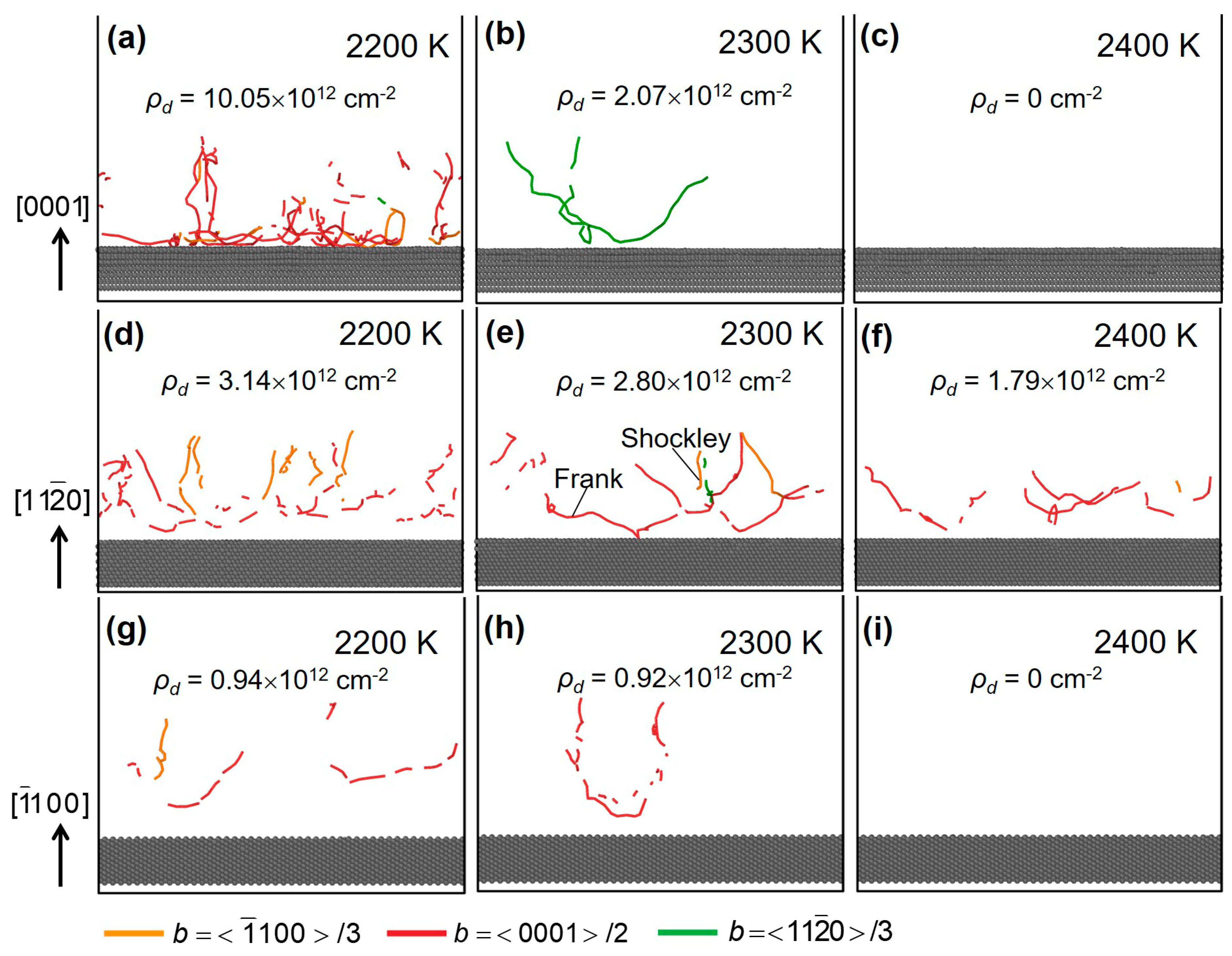
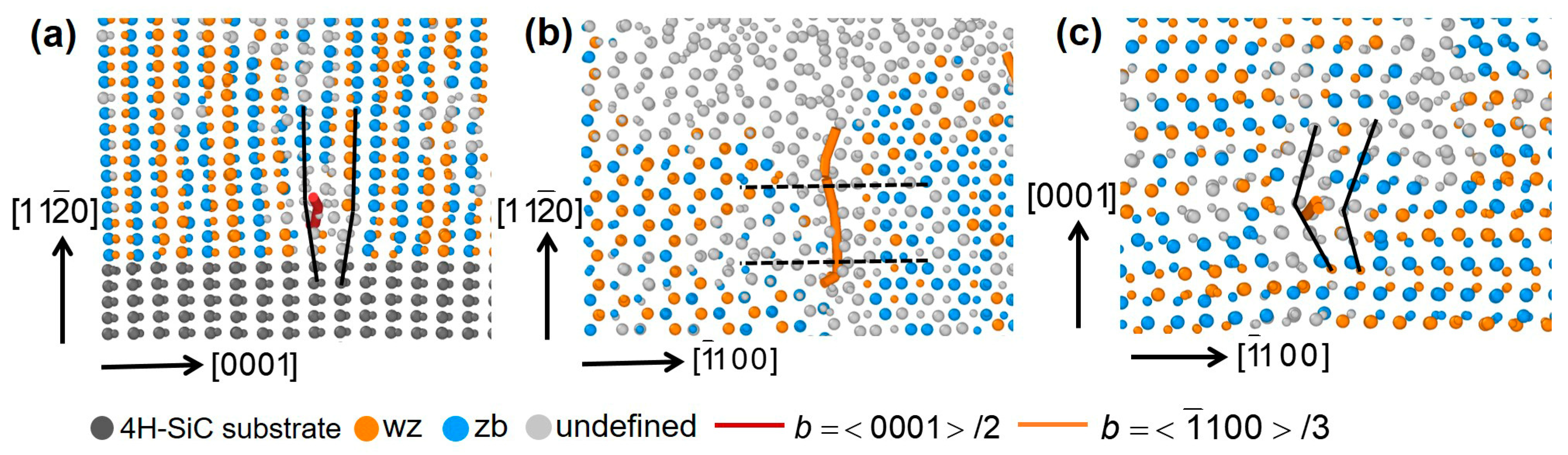
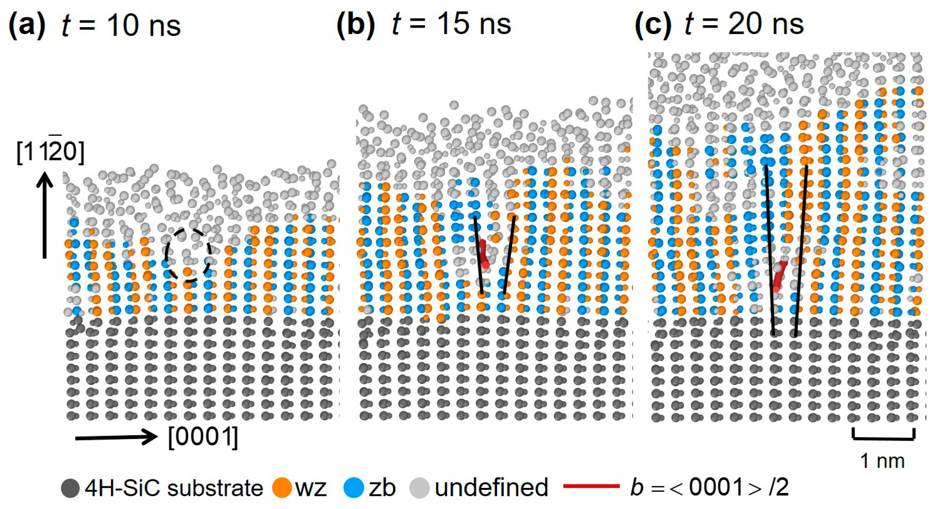
3.2. Dislocation Analysis

By using the DXA method implemented in the OVITO software, the spatial distribution, Burgers’ vector, and density of dislocations in the SiC crystals grown by vapor deposition with ( 0001 ) , ( 11 2 - 0 ) and ( 1 - 100 ) planes as surfaces and at different temperatures of the substrate (2200 K, 2300 K and 2400 K) were obtained and illustrated in Figure 5. It should be mentioned that the dislocation lines shown in Figure 5 display discontinuous features, which is not consistent with the requirement that the dislocation lines should not terminate inside the crystal in the theory of dislocations. This may be attributed to the presence of additional point defects in and around the core region of the dislocations in the crystals of the thin films obtained by MD vapor deposition simulations. The presence of these point defects can interfere with the identification of the dislocation lines by the DXA method.
Figure 5a–i show the distribution of dislocations in the SiC thin films deposited on the ( 0001 ) , ( 11 2 - 0 ) and ( 1 - 100 ) planes of 4H-SiC, respectively. The total length of the lines of dislocations identified for each model can be measured by the OVITO software as well. By dividing the total length of dislocations by the volume of the crystal grown in the film deposited, the density of dislocations ( ρ d ) can be calculated, and the values are indicated in the panels of Figure 5. One needs to pay attention to the density values of dislocations, as shown in Figure 5, which can be several orders higher than those measured in the film or boule obtained in experiments [40,41]. This discrepancy should mainly be attributed to the limited time and space scale of the MD simulations performed here, so an ultra-high deposition rate was adopted, and the thickness and volume of the films grown are much smaller than those obtained in experiments. Nevertheless, it can be found that the dislocation density in the thin films tends to decrease as the temperature of the substrate increases from 2200 K to 2400 K for vapor deposition growth on all three different substrate surfaces, which agrees well with the experimental observation that the density of dislocations in the thin film or boule generally decreases as the temperature of the substrate increases [40,41]. It is noteworthy that, at the same temperature of the substrate (e.g., 2200 K or 2300 K), the dislocation density in the crystal of thin film grown with the ( 1 - 100 ) plane as the substrate surface is lower than that of the cases with the ( 0001 ) and ( 11 2 - 0 ) planes as the substrate surface. Additionally, the results given in Figure 5 indicate that the dislocation lines in the grown crystals can have different Burgers’ vectors, which mainly include b   =   < 0001 > / 2 (thick red line), b   =   < 1 - 100 > / 3 (thick orange line) and b   =   < 11 2 - 0 > / 3 (thick green line).
With a more detailed analysis of the arrangement of atoms in and around the core of the dislocations identified by the DXA analysis, some extra features of the dislocations generated in the grown crystals can be revealed. Figure 6 shows the analysis of two typical dislocation segments in the dislocation network given by the DXA method in a SiC thin film grown by vapor deposition at a substrate with the ( 11 2 - 0 ) plane as the substrate surface and at the substrate temperature of 2300 K (see Figure 5e). Figure 6a illustrates a segment of dislocation with the Burgers’ vector b   =   < 0001 > / 2 (thick red line, as marked in Figure 5e correspondingly) and the distribution of the atoms around it. It can be seen that the line of dislocation is located on a ( 11 2 - 0 ) lattice plane, which is not considered a slip plane of 4H-SiC normally. There is an extra half plane of atoms above the core of the dislocation, as indicated by the thin black lines in Figure 6a. Therefore, this line of dislocation can be categorized as the Frank partial dislocation [33,42], and its formation mechanism will be discussed further in the next section.
Figure 6b,c illustrate another segment of dislocation with the Burgers’ vector b   =   < 1 - 100 > / 3 (the thick orange line, as marked in Figure 5e correspondingly) and the distribution of the atoms around it. The arrangement of atoms in the core region is rather disordered. It can be seen that this segment of dislocation lies exactly on a ( 0001 ) closest packed plane of 4H-SiC, which is a slip plane of 4H-SiC. Figure 6b indicates that the stacking characteristics of the atoms at the two sides of the dislocation line on this slip plane are different, with the left side showing the hexagonal wurtzite structure (wz) of the 4H-SiC lattice, while the right side shows the zinc blende structure (zb) of the 3C-SiC lattice, indicating that there is a relative slip displacement between the atoms on the left and right sides. A projected view of this segment of dislocation along the line of dislocation ( [ 11 2 - 0 ] ) can be obtained by slicing the region marked by the black dashed line in Figure 6b, and it is shown in Figure 6c. One can see that an extra plane of atoms can also be identified above the core of the dislocation line, as indicated by the thin black lines in Figure 6c. Taken together, this segment of dislocation can be identified as a Shockley partial dislocation [33,42].

4. Discussion

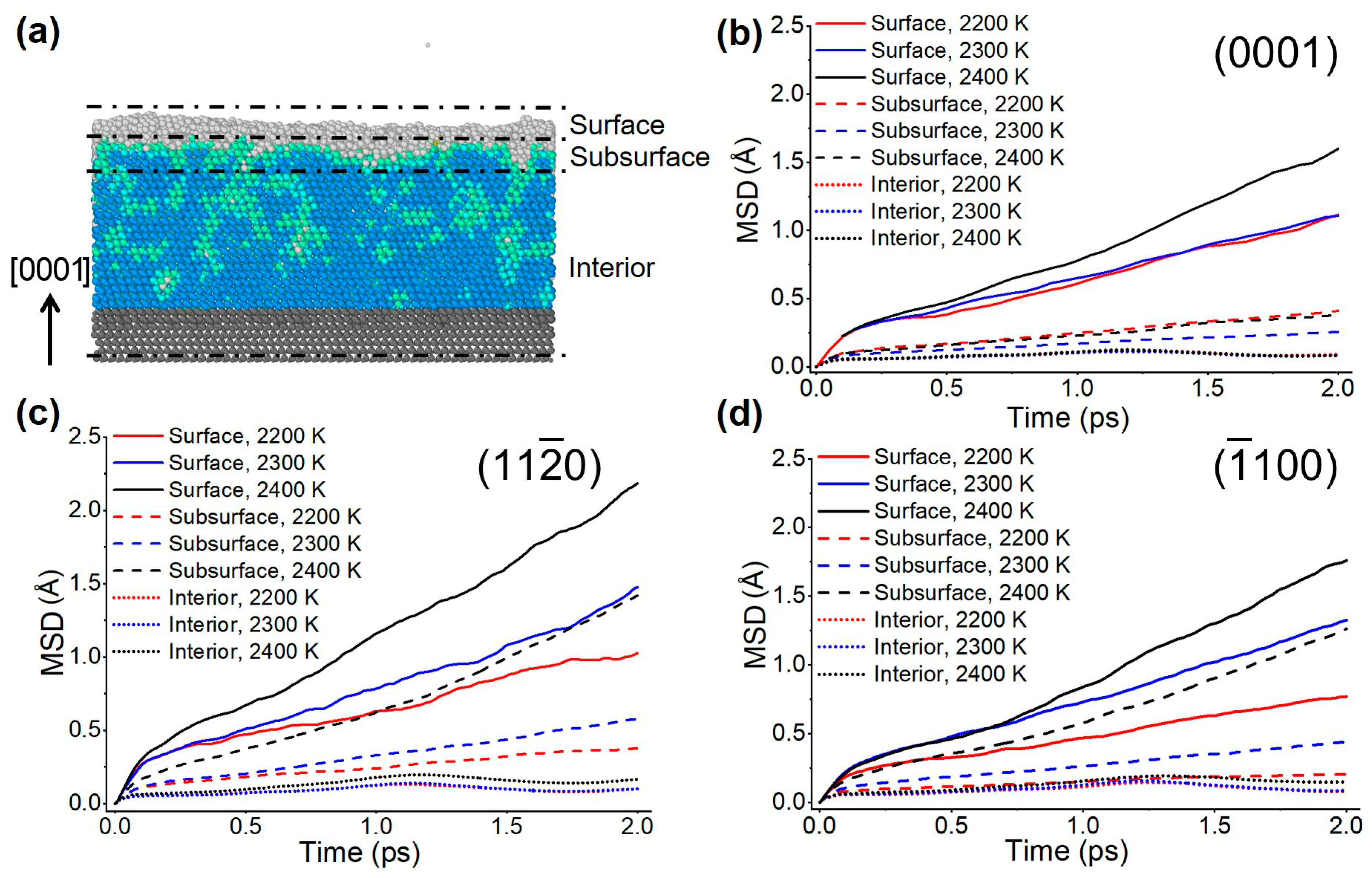
4.1. Kinetic Features of Nucleation and Growth of Crystals in Vapor Deposition Process

Figure 7 shows the snapshots of the atomistic arrangement of the deposited films at four different moments of 1 ns, 3 ns, 5 ns and 7 ns for the MD simulated vapor deposition processes with the temperature of 2300 K for substrate and with all the three selected surfaces of substrates. For the identification of crystals nucleated and grown in the thin film deposited during the vapor deposition processes, the coloring of the spheres corresponding to the atoms by using the IDS method, which is the same as that used in Figure 2, Figure 3 and Figure 4, was adopted in Figure 7. In addition, the detailed processes for the time evolution of the atomistic structure of the thin films in these vapor deposition processes can be further illustrated by the animations made for these vapor deposition processes (see the Supplementary video files S1–S3).
At the time of 1 ns, the adatoms have not yet completely covered the surface on all three substrates, and the nucleation of crystal has not yet occurred at this moment (see Figure 7a,e,i). With the atoms in the gas phase continuing to fall onto the substrates, the surfaces of substrates were completely covered by the adatoms at the time of 3 ns. One can see that a small number of embryos of SiC crystal can be found on the surface of substrates at this moment (see Figure 7b,f,j). At the time of 5–7 ns, as the thickness of the deposited thin film increased uniformly along the surface, the regions of crystals nucleated were extended and connected to cover the entire surface, and the thickness of the crystals increased continuously to give the growth of the crystals on the substrates. It is noteworthy that both the nucleation and growth of the crystals basically happened in the area well below the top surface layer, while the arrangement of atoms on the top surface layer remains to be disordered in the vapor deposition processes. This is particularly true for the vapor deposition processes with the non-closest packed plane of ( 11 2 - 0 ) and ( 1 - 100 ) as substrate surface, as one can see that the thickness of the surface layers with the disordered atomistic structure is relatively large (about 0.5 nm) in these cases (see Figure 7h,l). The growth of the crystals was found to be always realized by rearrangement of the disordered atoms in the subsurface area to form the ordered crystal structure in the subsequent deposition processes (see Figure 2, Figure 3 and Figure 4). The adoption of this kind of subsurface nucleation and growth mode presented here should be closely related to the very high deposition rate used in our MD simulation of the vapor deposition processes. Nevertheless, we would like to suggest that, depending on the thermodynamic factors such as the temperature of the substrate, deposition rate, and surface chemical environment, the subsurface nucleation and growth mode might still be functioning even in the experimental vapor deposition processes for the growth of the SiC crystals or epitaxial films, and is worth further examination and analysis in the future.

4.2. Mechanism of Dislocation Formation

Figure 8 shows the time series images (10 ns, 15 ns and 20 ns) of the arrangement of atoms in a local area of the SiC thin films during the deposition process with the ( 11 2 - 0 ) plane as the substrate surface and at the temperature of 2300 K for substrate (see Figure 3b for the whole view of this thin film in the final state). From Figure 8a, it can be seen that at the time of 10 ns, a crystalline zone of a certain thickness has been formed in the deposited film, and there is no dislocation in this local area of the crystal grown at this moment. One can also find that there is a disordered amorphous layer of about 1 nm thick on top of the crystalline zone, which is consistent with the subsurface nucleation and growth mode given in the above analysis. At the same time, a “V” shaped region can be seen at the boundary between the surface disordered amorphous layer and the crystalline zone. At the time of 15 ns (Figure 8b) and 20 ns (Figure 8c), the atoms within the previously disordered amorphous layer gradually arrange themselves to an orderly crystalline structure, resulting in an outward extension and thickening of the crystalline zone. Meanwhile, an extra half plane of atoms can be found in this extended crystalline zone at the location corresponding to the above “V” shaped region, as shown by the thin black lines in Figure 8b,c), and it can be identified to be a Frank partial dislocation with Burgers vector of b   =   < 0001 > / 2 . Based on this time series analysis, we speculate that the formation of the Frank partial dislocation can be attributed to the following factors. Firstly, the sites for nucleation and the frontier of growth of the SiC crystal mainly locate in the subsurface region at the surface amorphous layer. Secondly, the density of atoms deposited in the “V” shaped region can be relatively higher than that of the surrounding region and the ideal 4H-SiC lattice. Thirdly, it is likely that the atoms in the subsurface region are not able to diffuse outward timely during the crystallization process. Bring together, an extra half plane of atoms inside the crystal can then be formed to give the Frank partial dislocation in the crystal, as shown in Figure 8.
In order to further analyze the influence of the diffusivity of atoms in the deposited thin film on dislocation formation, we have calculated the diffusion behavior of atoms in regions of different depths of the deposited thin film. A schematic illustration of the partitioning of the deposited thin film and substrate along the growth direction is given in Figure 9a. The mean square displacement (MSD) calculations were performed for each region of all the SiC films obtained by vapor deposition growth simulations. The variation of the MSDs of atoms with time for all these regions is shown in Figure 9b–d. It can be seen that, after a short initial period of time (about 0.2 ps), an almost linear variation of MSD with time will be given on all these curves, indicating that a steady state diffusion state is reached for the diffusion of atoms in all of these regions. For the “Surface” and “Subsurface” regions, the higher the substrate temperature, the larger the slope of the MSD curves, i.e., the higher the diffusivity of the atoms in the specific regions. The slopes of the MSD curves for the “Surface” regions are the largest, followed by those of the “Subsurface” regions. For the “Interior” regions, the MSD of the atoms almost does not vary with time, indicating that the atoms in the SiC crystals grown are rather inactive in diffusion.
According to these results, the atoms in the “V” shaped region in Figure 8a are much less active in diffusion than the atoms on the top surface layer of this film in the vapor deposition process. If the atoms deposited in this region happen to have a relatively higher density, they can form an extra half plane of atoms rather easily on crystallization, which in turn forms a Frank partial dislocation, as shown in Figure 8b,c. It suggests that, by changing the temperature of the substrate, the diffusivity of atoms in the “Surface” and “Subsurface” regions will be significantly altered, and the density of dislocations generated in the thin film grown by the vapor deposition method shall be largely changed accordingly. This is consistent with the decrease of dislocation density in the films by the increase of the temperature of the substrate from 2200 K to 2400 K for all the substrates with different lattice planes as the surface of substrates, as given in Figure 5.

5. Conclusions

We investigated the vapor deposition growth of SiC crystal on a 4H-SiC substrate and the relevant physical and chemical characteristics of this growth process by using the computer MD simulation method. By selecting the basal plane ( 0001 ) , non-basal planes of ( 11 2 - 0 ) and ( 1 - 100 ) as the surface of substrates, and applying different temperatures (2200 K, 2300 K and 2400 K) for the substrates, we examined the effects of the lattice plane of the substrate surface and the temperature of the substrate on the characteristics of the formation of polytypes and dislocations in the SiC thin film deposited on 4H-SiC substrate.
The results show that the 3C-SiC single crystal was formed in the deposited thin film grown on substrates with ( 0001 ) plane as the surface, while the 4H-SiC single crystal was obtained in the deposited thin film grown on substrates with non-basal planes of ( 11 2 - 0 ) and ( 1 - 100 ) plane as the surface. There can be a certain density of dislocations with various Burgers’ vectors generated in the crystals obtained by vapor deposition, including Frank partial dislocations and Shockley partial dislocations. An increase in the temperature of the substrate is beneficial for the reduction of the dislocation density in the crystals of deposited thin films, which is in good agreement with the experimental observations. The analysis shows that the growth of crystal on the substrate in the vapor deposition process is accomplished by a subsurface nucleation and growth mode for all the vapor deposition processes studied. In addition, we found that the formation of dislocations in the crystals grown by vapor deposition is closely related to the diffusivity of the atoms in the surface and subsurface layers of the deposited film.
Due to the simplification of models used in this work, the results presented here are rather preliminary. Nevertheless, these results can serve as a reference for the design of processing parameters, such as the temperature of substrate and surface of the substrate, in experimental vapor deposition growth of SiC single crystals with selected polytypes as well as reduced density of dislocations. Moreover, it gives a good illustration that the MD simulation method can be very helpful for gaining a deep understanding of the various aspects of physical and chemical characteristics of the vapor deposition growth process for SiC.

Supplementary Materials

The following supporting information can be downloaded at: https://www.mdpi.com/article/10.3390/cryst13050715/s1, Video S1: Animation of the initial stage (0~7 ns) of the vapor deposition growth of SiC thin film on 4H-SiC substrate with ( 0001 ) plane as surface and at substrate temperature of 2300 K by molecular dynamics simulation (the coloring style is the same as Figure 7); Video S2: Animation of the initial stage (0~7 ns) of the vapor deposition growth of SiC thin film on 4H-SiC substrate with ( 11 2 - 0 ) plane as surface and at substrate temperature of 2300 K by molecular dynamics simulation (the coloring style is the same as Figure 7); Video S3: Animation of the initial stage (0~7 ns) of the vapor deposition growth of SiC thin film on 4H-SiC substrate with ( 1 - 100 ) plane as surface and at substrate temperature of 2300 K by molecular dynamics simulation (the coloring style is the same as Figure 7).

Author Contributions

Methodology, K.W.; software, K.W.; investigation, K.W.; writing—original draft, K.W.; project administration, Q.M. and S.Z.; resources, Q.M. and B.G.; data curation, H.L.; funding acquisition, H.L. and L.W.; writing—review and editing, S.Z., B.G., C.L., S.L. and L.W.; Supervision, C.L., S.L. and L.W. All authors have read and agreed to the published version of the manuscript.

Funding

This research was funded by Fundamental Research Funds for the Central Universities of China, grant numbers 2042019kf0036 and 2042020gf0006.

Data Availability Statement

No new data were created or analyzed in this study. Data sharing is not applicable to this article.

Acknowledgments

This work was supported by the Fundamental Research Funds for the Central Universities of China (2042019kf0036, 2042020gf0006). The numerical calculations in this paper have been done on the supercomputing system in the Supercomputing Centre of Wuhan University.

Conflicts of Interest

The authors declare no conflict of interest.

References

  1. Kimoto, T. Bulk and epitaxial growth of silicon carbide. Prog. Cryst. Growth Charact. Mater. 2016, 62, 329–351. [Google Scholar] [CrossRef]
  2. Chaussende, D.; Wellmann, P.J.; Pons, M. Status of SiC bulk growth processes. J. Phys. D Appl. Phys. 2007, 40, 6150–6158. [Google Scholar] [CrossRef]
  3. Matsunami, H.; Kimoto, T. Step-controlled epitaxial growth of SiC: High quality homoepitaxy. Mater. Sci. Eng. R Rep. 1997, 20, 125–166. [Google Scholar] [CrossRef]
  4. Song, B.; Gao, B.; Han, P.; Yu, Y.; Tang, X. Numerical Simulation of Gas Phase Reaction for Epitaxial Chemical Vapor Deposition of Silicon Carbide by Methyltrichlorosilane in Horizontal Hot-Wall Reactor. Materials 2021, 14, 7532. [Google Scholar] [CrossRef] [PubMed]
  5. Sumakeris, J.J.; Leonard, R.T.; Deyneka, E.; Khlebnikov, Y. Dislocation Characterization in 4H-SiC Crystals. Mater. Sci. Forum 2016, 858, 393–396. [Google Scholar] [CrossRef]
  6. Nakano, T.; Shinagawa, N.; Yabu, M.; Ohtani, N. Formation and multiplication of basal plane dislocations during physical vapor transport growth of 4H-SiC crystals. J. Cryst. Growth 2019, 516, 51–56. [Google Scholar] [CrossRef]
  7. Xu, M.; Girish, Y.R.; Rakesh, K.P. Recent advances and challenges in silicon carbide (SiC) ceramic nanoarchitectures and their applications. Mater. Today Commun. 2021, 28, 102533. [Google Scholar] [CrossRef]
  8. Meng, B.; Qiu, P.; Yuan, D.; Xu, S. Influence of microstructure on the diamond-machinability of hot-pressed silicon carbide: A molecular dynamics study. Ceram. Int. 2019, 45, 22872–22879. [Google Scholar] [CrossRef]
  9. Semmelroth, K.; Krieger, M.; Pensl, G.; Nagasawa, H. Growth of cubic SiC single crystals by the physical vapor transport technique. J. Cryst. Growth 2007, 308, 241–246. [Google Scholar] [CrossRef]
  10. Seki, K.; Alexander, S.; Kozawa, S. Polytype-selective growth of SiC by supersaturation control in solution growth. J. Cryst. Growth 2012, 360, 176–180. [Google Scholar] [CrossRef]
  11. Inomata, Y.; Inoue, Z.; Mitomo, M.; Suzuki, H. Relation Between Growth Temperature and the Structure of SiC Crystals Grown by the Sublimation Method. J. Ceram. Assoc. Jpn. 1968, 76, 313–319. [Google Scholar] [CrossRef]
  12. Chen, X.; Zhao, H.; Ai, W. Study on the competitive growth mechanism of SiC polytypes using Kinetic Monte Carlo method. J. Cryst. Growth 2021, 559, 126042. [Google Scholar] [CrossRef]
  13. Yang, Y.B.; Wang, J.; Wang, Y.M. Thermal stress simulation of optimized SiC single crystal growth crucible structure. J. Cryst. Growth 2018, 504, 31–36. [Google Scholar] [CrossRef]
  14. Samant, A.V.; Pirouz, P. Activation parameters for dislocation glide in α-SiC. Int. J. Refract. Metals Hard Mater. 1998, 16, 277–289. [Google Scholar] [CrossRef]
  15. Selder, M.; Kadinski, L.; Durst, F.; Hofmann, D. Global modeling of the SiC sublimation growth process: Prediction of thermoelastic stress and control of growth conditions. J. Cryst. Growth 2001, 226, 501–510. [Google Scholar] [CrossRef]
  16. Steiner, J.; Arzig, M.; Denisov, A.; Wellmann, P.J. Impact of Varying Parameters on the Temperature Gradients in 100 mm Silicon Carbide Bulk Growth in a Computer Simulation Validated by Experimental Results. Cryst. Res. Technol. 2020, 55, 1900121. [Google Scholar] [CrossRef]
  17. Wellmann, P.J. Review of SiC crystal growth technology. Semicond. Sci. Technol. 2018, 33, 103001. [Google Scholar] [CrossRef]
  18. Xue, L.; Feng, G.; Wu, G.; Wang, S.; Li, R.; Han, X.; Sun, Y.; Liu, S. Study of the deposition of nanopillar-patterned 4H-SiC by molecular dynamics simulation. Appl. Surf. Sci. 2022, 579, 152209. [Google Scholar] [CrossRef]
  19. Liu, B.; Yu, Y.; Tang, X.; Gao, B. Influence of silicon melt convection on interface instability in large-size silicon carbide solution growth. J. Cryst. Growth 2019, 527, 125248. [Google Scholar] [CrossRef]
  20. Kang, K.-H.; Eun, T.; Jun, M.-C.; Lee, B.-J. Governing factors for the formation of 4H or 6H-SiC polytype during SiC crystal growth: An atomistic computational approach. J. Cryst. Growth 2014, 389, 120–133. [Google Scholar] [CrossRef]
  21. Vashishta, P.; Kalia, R.K.; Nakano, A.; Rino, J.P. Interaction potential for silicon carbide: A molecular dynamics study of elastic constants and vibrational density of states for crystalline and amorphous silicon carbide. J. Appl. Phys. 2007, 101, 103515. [Google Scholar] [CrossRef]
  22. Tersoff, J. Modeling solid-state chemistry: Interatomic potentials for multicomponent systems. Phys. Rev. B 1989, 39, 5566–5568. [Google Scholar] [CrossRef]
  23. Jiang, C.; Morgan, D.; Szlufarska, I. Carbon tri-interstitial defect: A model for the DII center. Phys. Rev. B 2012, 86, 144118. [Google Scholar] [CrossRef]
  24. Plimpton, S. Fast Parallel Algorithms for Short-Range Molecular Dynamics. J. Comput. Phys 1995, 117, 1–19. [Google Scholar] [CrossRef]
  25. Parrinello, M.; Rahman, A. Crystal Structure and Pair Potentials: A Molecular-Dynamics Study. Phys. Rev. Lett. 1980, 45, 1196–1199. [Google Scholar] [CrossRef]
  26. Nose, S. A Unified Formulation of the Constant Temperature Molecular-Dynamics Methods. J. Chem. Phys. 1984, 81, 511–519. [Google Scholar] [CrossRef]
  27. Nose, S. A molecular dynamics method for simulations in the canonical ensemble. Mol. Phys. 1984, 52, 255–268. [Google Scholar] [CrossRef]
  28. Hoover, W.G. Canonical dynamics: Equilibrium phase-space distributions. Phys. Rev. A 1985, 31, 1695–1697. [Google Scholar] [CrossRef] [PubMed]
  29. Stukowski, A. Visualization and analysis of atomistic simulation data with OVITO—The Open Visualization Tool. Modell. Simul. Mater. Sci. Eng. 2010, 18, 015012. [Google Scholar] [CrossRef]
  30. Maras, E.; Trushin, O.; Stukowski, A.; Ala-Nissila, T.; Jónsson, H. Global transition path search for dislocation formation in Ge on Si(001). Comput. Phys. Commun. 2016, 205, 13–21. [Google Scholar] [CrossRef]
  31. Stukowski, A.; Albe, K. Extracting dislocations and non-dislocation crystal defects from atomistic simulation data. Modell. Simul. Mater. Sci. Eng. 2010, 18, 085001. [Google Scholar] [CrossRef]
  32. Gruber, J.; Zhou, X.W.; Jones, R.E.; Lee, S.R.; Tucker, G.J. Molecular dynamics studies of defect formation during heteroepitaxial growth of InGaN alloys on (0001) GaN surfaces. J. Appl. Phys. 2017, 121, 195301. [Google Scholar] [CrossRef]
  33. Gruber, K.J.; Zhou, X.W.; Jones, R.E.; Lee, S.R.; Tucker, G.J. Molecular dynamics studies of InGaN growth on nonpolar (11–20) GaN surfaces. Phys. Rev. Mater. 2018, 2, 013402. [Google Scholar] [CrossRef]
  34. Zhang, L.; Li, L.; Wang, Y.; Suo, Y.; Liu, S.; Gan, Z. Atomic simulation of AlGaN film deposition on AlN template. Mol. Phys. 2019, 118, 1702728. [Google Scholar] [CrossRef]
  35. Wang, B.; Yin, J.; Chen, D.; Long, X. Optical and surface properties of 3C–SiC thin epitaxial films grown at different temperatures on 4H–SiC substrates. Superlattices Microstruct. 2021, 156, 106960. [Google Scholar] [CrossRef]
  36. Takahashi, N.O.J. Modified-Lely SiC Crystals Grownin [1-100] and [11-20] Directions. Phys. Status Solidi (b) 1997, 202, 163–175. [Google Scholar] [CrossRef]
  37. Jepps, N.W.; Page, T.F. Polytypic transformations in silicon carbide. Prog. Cryst. Growth Charact. Mater. 1983, 7, 259–307. [Google Scholar] [CrossRef]
  38. Yoo, W.S.; Matsunami, H. Solid-State Phase Transformation in Cubic Silicon Carbide. Jpn. J. Appl. Phys. 1991, 30, 545. [Google Scholar] [CrossRef]
  39. Shi, Y.; Jokubavicius, V.; Höjer, P. A comparative study of high-quality C-face and Si-face 3C-SiC(1 1 1) grown on off-oriented 4H-SiC substrates. J. Phys. D Appl. Phys. 2019, 52, 345103. [Google Scholar] [CrossRef]
  40. Hoshino, N.; Kamata, I.; Kanda, T.; Tokuda, Y.; Kuno, H. Reduction in dislocation densities in 4H-SiC bulk crystal grown at high growth rate by high-temperature gas-source method. Appl. Phys. Express. 2020, 13, 095502. [Google Scholar] [CrossRef]
  41. Sakwe, S.A.; Stockmeier, M.; Hens, P.; Müller, R. Bulk growth of SiC—Review on advances of SiC vapor growth for improved doping and systematic study on dislocation evolution. Phys. Status Solidi (b) 2008, 245, 1239–1256. [Google Scholar] [CrossRef]
  42. Anderson, P.M.; Hirth, J.P.; Lothe, J. Theory of Dislocations, 3rd ed.; Cambridge University Press: New York, NY, USA, 2017; pp. 602–626. [Google Scholar]
Figure 1. Atomistic models for the 4H-SiC substrate: (a) the substrate with ( 0001 ) plane as surface, (b) the substrate with ( 11 2 - 0 ) plane as surface, (c) the substrate with ( 1 - 100 ) plane as surface.
Crystals 13 00715 g001
Figure 2. Atomistic structure of SiC thin films grown by vapor deposition on substrates of 4H-SiC with the ( 0001 ) Si-terminated plane as the surface, while the temperature of substrate was given as 2200 K (a), 2300 K (b) and 2400 K (c), respectively. (d) is the two views of detailed atomistic arrangement of a local area of 1 nm thick sliced from the deposited SiC thin film in (b) parallel to the ( 11 2 - 0 ) and the ( 1 ¯ 100 ) planes of the substrate, respectively. In (d), the stacking sequence (ABCABC) of the closest packed Si-C diatomic layer is indicated, with the dotted line marked to guide the eye. The coloring of the spheres corresponding to the atoms is based on the classification of the seven local structural features of atoms given by the IDS method (see Section 2.3), and the dark gray spheres represent atoms in the substrate.
Crystals 13 00715 g002
Figure 3. Atomistic structure of SiC thin films grown by vapor deposition on 4H-SiC substrate with ( 11 2 - 0 ) plane as the surface, while the temperature of substrate was given as 2200 K (a), 2300 K (b) and 2400 K (c), respectively. (d) is the two views of detailed atomistic arrangement of a local area of 1 nm thick sliced from the SiC thin film parallel to the ( 11 2 - 0 ) and ( 1 - 100 ) planes of the substrate, respectively. In (d), the stacking sequence (ABCBABCB) of the closest packed Si-C diatomic layer is indicated, with the dotted line marked to guide the eye. The coloring of the spheres corresponding to the atoms is based on the classification of the seven local structural features of atoms given by the IDS method (see Section 2.3), and the dark gray spheres represent atoms in the substrate.
Crystals 13 00715 g003
Figure 4. Atomistic structure of SiC thin films grown by vapor deposition on 4H-SiC substrate with ( 1 - 100 ) plane as the surface, while the temperature of substrate was given as 2200 K (a), 2300 K (b) and 2400 K (c), respectively. (d) is the two views of detailed atomistic arrangement of a local area of 1 nm thick sliced from the deposited SiC film in (b) parallel to the ( 11 2 - 0 ) and ( 1 - 100 ) planes of the substrate, respectively. In (d), the stacking sequence (ABCBABCB) of the closest packed Si-C diatomic layer is indicated, with the dotted line marked to guide the eye. The coloring of the spheres corresponding to the atoms is based on the classification of the seven local structural features of atoms given by the IDS method (see Section 2.3), and the dark gray spheres represent atoms in the substrate.
Crystals 13 00715 g004
Figure 5. Spatial distribution, Burgers’ vector and density ( ρ d ) of dislocations in SiC crystals of the thin films grown by vapor deposition with different planes of 4H-SiC as the surface of the substrate and at different temperatures of substrate: (a) ( 0001 ) plane, 2200 K, (b) ( 0001 ) plane, 2300 K, (c) ( 0001 ) plane, 2400 K, (d) ( 11 2 - 0 ) plane, 2200 K, (e) ( 11 2 - 0 ) plane, 2300 K, (f) ( 11 2 - 0 ) plane, 2400 K, (g) ( 1 - 100 ) plane, 2200 K, (h) ( 1 - 100 ) plane, 2300 K, (i) ( 1 - 100 ) plane, 2400 K. The dark gray spheres represent atoms of the substrate. The thick lines indicate the dislocations, which are colored differently to distinguish their Burgers vectors, as shown at the bottom of the figure.
Crystals 13 00715 g005
Figure 6. The arrangement of atoms in and around the core region of the segment of a Frank partial dislocation (a) and the segment of a Shockley partial dislocation (b,c), while both segments are sliced from the SiC thin film grown by vapor deposition with the ( 11 2 - 0 ) plane as the surface of substrate and at a temperature of 2300 K for substrate (marked in Figure 5e). The spheres colored orange (“wz”) or blue (“zb”) represent the atoms that have a local atomistic structure corresponding to the wurtzite structure (hexagonal structure) or the zinc blende structure (cubic structure), respectively. The spheres colored light gray (“undefined”) represent the atoms that have a local atomistic structure that does not belong to the above two structures. The dark gray spheres represent atoms in the substrate.
Crystals 13 00715 g006
Figure 7. Images of SiC thin films grown by vapor deposition on 4H-SiC substrates with different lattice planes as substrate surfaces and at four different times in the vapor deposition processes at 2300 K: (a) ( 0 001 ) plane, 1 ns, (b) ( 0 001 ) plane, 3 ns, (c) ( 0 001 ) plane, 5 ns, (d) ( 0 001 ) plane, 7 ns, (e) ( 11 2 - 0 ) plane, 1 ns, (f) ( 11 2 - 0 ) plane, 3 ns, (g) ( 11 2 - 0 ) plane, 5 ns, (h) ( 11 2 - 0 ) plane, 7 ns, (i) ( 1 - 100 ) plane, 1 ns, (j) ( 1 - 100 ) plane, 3 ns, (k) ( 1 - 100 ) plane, 5 ns, (l) ( 1 - 100 ) plane, 7 ns. The coloring of the spheres corresponding to the atoms is based on the classification of the seven local structural features of atoms given by the IDS method (see Section 2.3), and the dark gray spheres represent atoms in the substrate.
Crystals 13 00715 g007
Figure 8. Time series images of the formation of a Frank partial dislocation with Burgers’ vector b   =   < 0001 > / 2 during the vapor deposition growth process on 4H-SiC substrate with ( 11 2 - 0 ) plane as the surface and at temperature of 2300 K for substrate: (a) t = 10 ns, (b) t = 15 ns, (c) t = 20 ns. The spheres colored orange (“wz”) or blue (“zb”) represent the atoms that have a local atomistic structure corresponding to the wurtzite structure (hexagonal structure) or the zinc blende structure (cubic structure), respectively. The spheres colored light gray (“undefined”) represent the atoms with a local atomistic structure that does not belong to the above two structures. The dark gray spheres represent atoms in the substrate, and dislocations are marked by thick red lines. The dashed circle in (a) marks the “V” shaped region where the dislocation nucleates. In all the images, only a thin slice of 1 nm thickness was intercepted for the projected view.
Crystals 13 00715 g008
Figure 9. Calculation of mean square displacement (MSD) of atoms in three different regions for the SiC thin films grown by vapor deposition on substrate of 4H-SiC with different lattice planes as the surface and at different substrate temperatures. (a) Schematic illustration of partitioning of a SiC thin film to three different regions: “Surface” indicates the amorphous layer on the top of the surface of the thin film deposited, “Interior” indicates the internal region of the SiC crystal, including the substrate and the crystal in the deposited film (excluding the immobile atoms at the bottom of the substrate), and “Subsurface” indicates the interface region between the amorphous layer and the internal crystal. The coloring of spheres which represent atoms in the model of SiC thin film here is the same as that of Figure 2. (bd) MSD curves for each region of the SiC thin films grown by vapor deposition on 4H-SiC substrate with ( 0001 ) , ( 11 2 - 0 ) and ( 1 ¯ 100 ) plane as the surface, respectively.
Crystals 13 00715 g009
Disclaimer/Publisher’s Note: The statements, opinions and data contained in all publications are solely those of the individual author(s) and contributor(s) and not of MDPI and/or the editor(s). MDPI and/or the editor(s) disclaim responsibility for any injury to people or property resulting from any ideas, methods, instructions or products referred to in the content.

