
Deep Ultraviolet Photodetector: Materials and Devices


 ,
,
Abstract
:1. Introduction
2. DUV Photodetectors Based on Boron Nitride Material
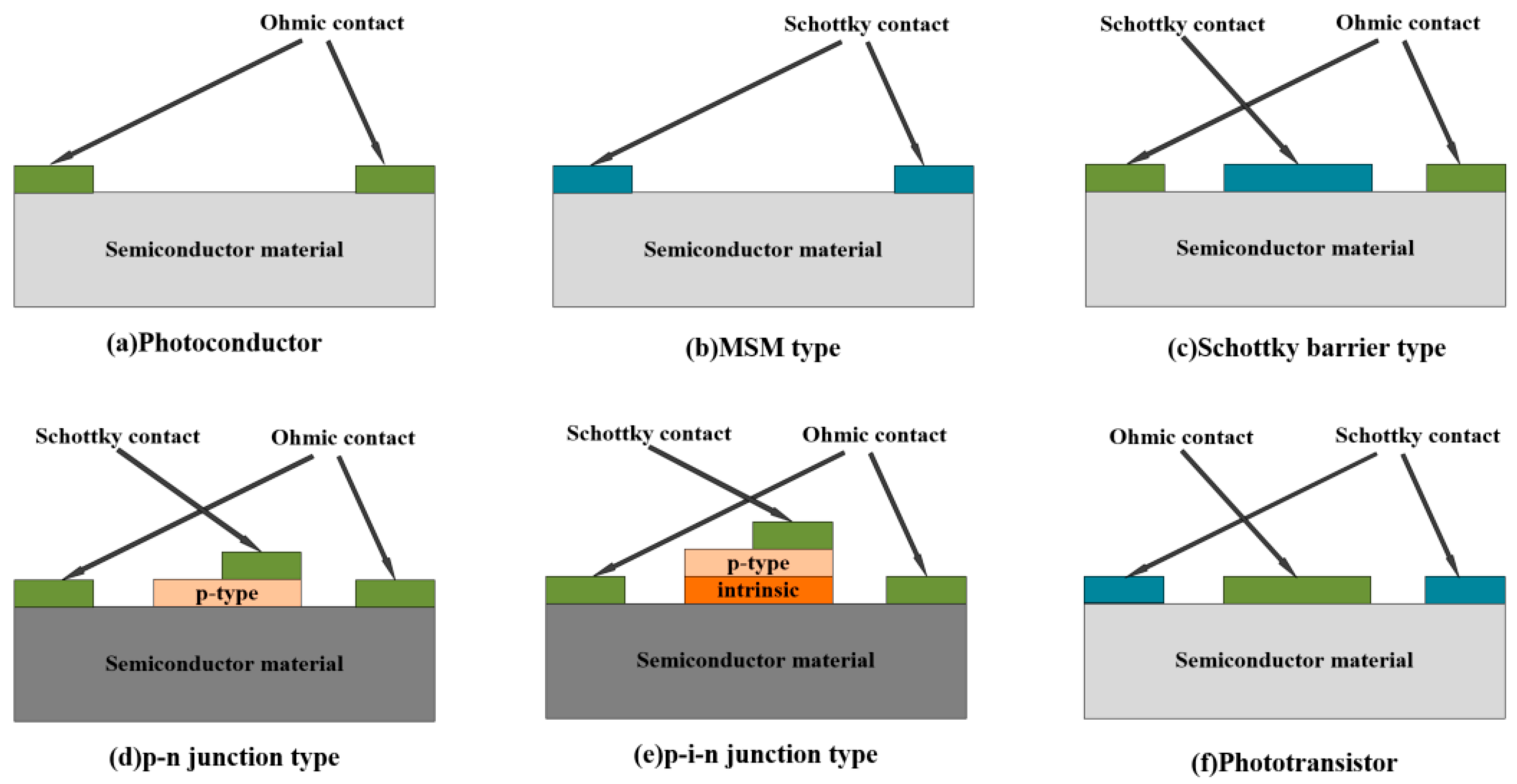
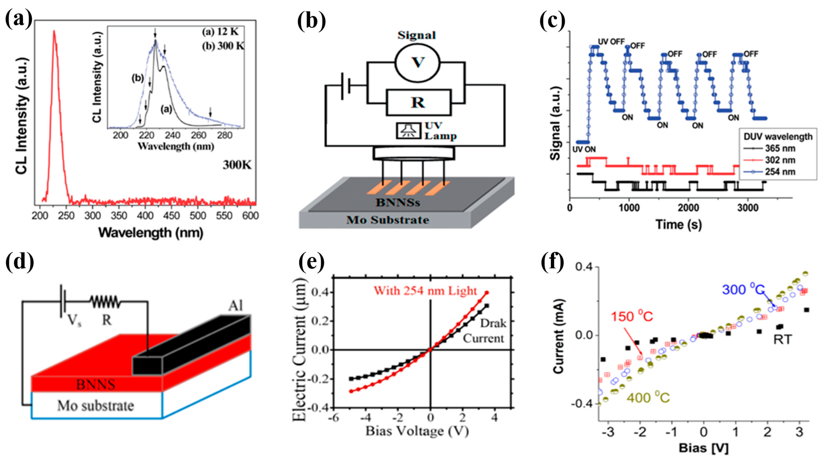
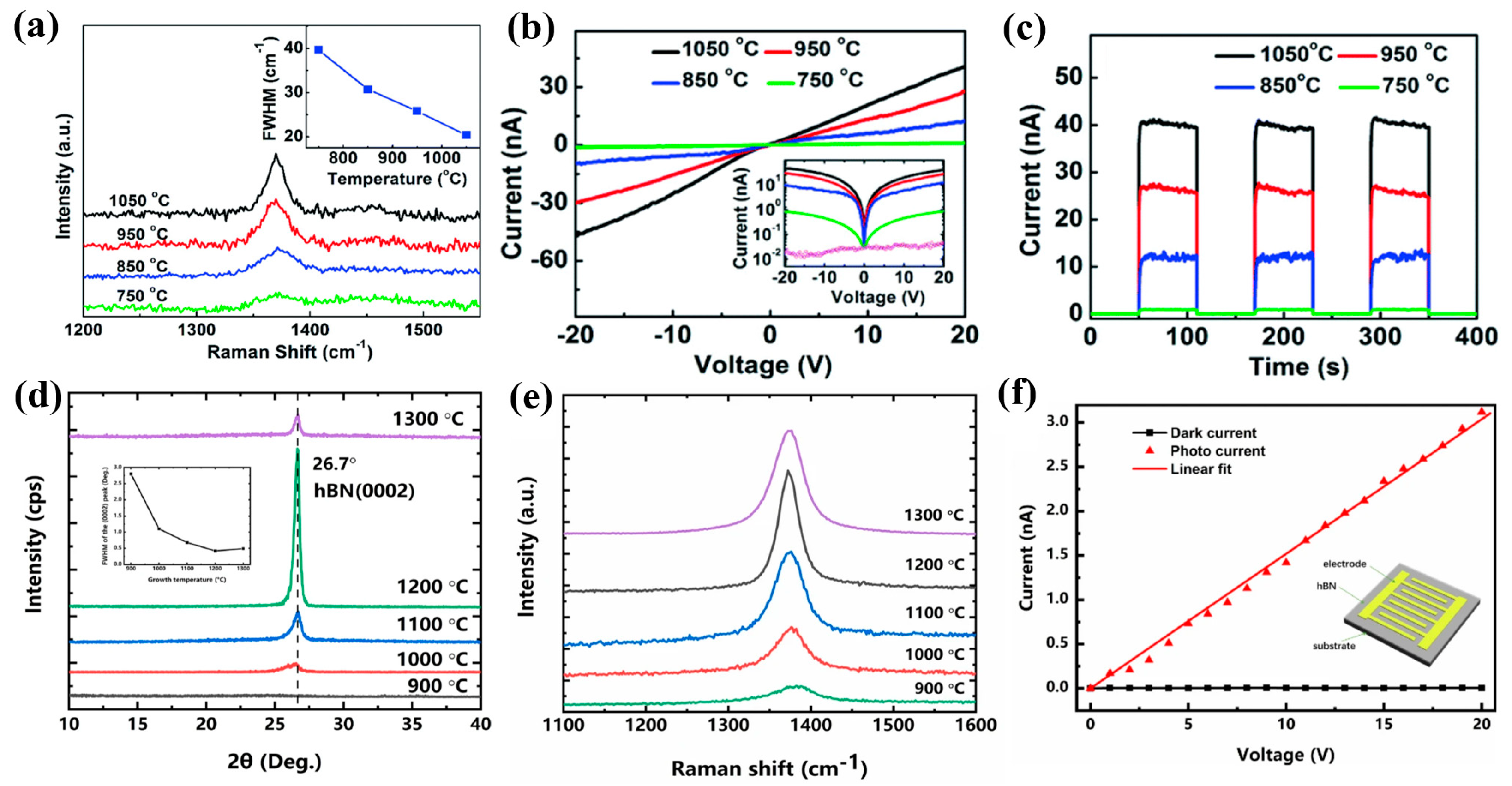
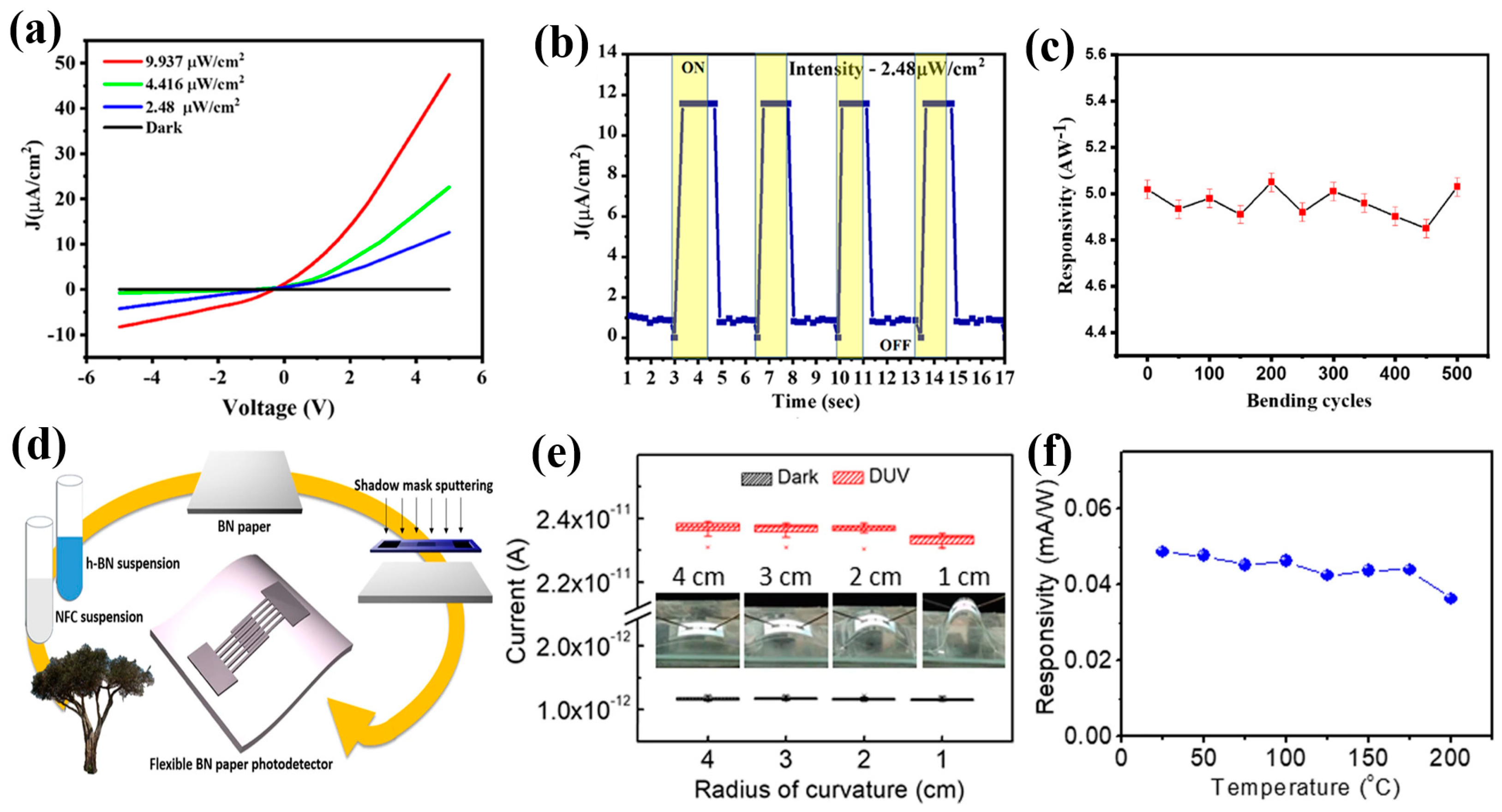
2.1. BN Nanostructures
2.2. BN Thin Films

2.3. BN Heterostructures
3. DUV Photodetectors Based on Aluminum Nitride Material
3.1. AlN Nanostructures
3.2. AlN Thin Films
3.3. AlN Heterostructures
4. DUV PDs Based on Aluminum Gallium Nitride Material
4.1. AlGaN Nanostructures
4.2. AlGaN Thin Films
4.3. AlGaN Heterostructures
5. DUV PDs Based on Gallium Oxide Material
5.1. Ga2O3 Nanostructures
5.2. Ga2O3 Thin Films
5.3. Ga2O3 Heterostructures
6. DUV PDs Based on Diamond Material
6.1. Diamond Thin Films
6.2. Diamond Heterostructures

7. Conclusions and Challenges
Author Contributions
Funding
Data Availability Statement
Conflicts of Interest
References
- Yu, X.; Marks, T.J.; Facchetti, A. Metal oxides for optoelectronic applications. Nat. Mater. 2016, 15, 383–396. [Google Scholar] [CrossRef] [PubMed]
- Lin, Q.; Armin, A.; Burn, P.L.; Meredith, P. Filterless narrowband visible photodetectors. Nat. Photon 2015, 9, 687–694. [Google Scholar] [CrossRef]
- Monroy, E.; Omnès, F.; Calle, F.J. Wide-bandgap semiconductor ultraviolet photodetectors. Semicond. Sci. Technol. 2003, 18, R33–R51. [Google Scholar] [CrossRef]
- Razeghi, M. Short-wavelength solar-blind detectors—Status, prospects, and markets. Proc. IEEE 2002, 90, 1006–1014. [Google Scholar] [CrossRef]
- Xie, C.; Lu, X.; Tong, X.; Zhang, Z.; Liang, F.; Liang, L.; Luo, L.; Wu, Y. Recent Progress in Solar-Blind Deep-Ultraviolet Photodetectors Based on Inorganic Ultrawide Bandgap Semiconductors. Adv. Funct. Mater. 2019, 29, 1806006. [Google Scholar] [CrossRef]
- Shang, H.; Dai, M.; Gao, F.; Yang, H.; Hu, P.; Jia, D.; Zhou, Y.; Chen, H. Progress in Inorganic Ultraviolet Photoelectric Materials. Mater. China 2019, 38, 875–886. [Google Scholar]
- Yang, J.; Liu, K.; Chen, X.; Shen, D. Recent advances in optoelectronic and microelectronic devices based on ultrawide-bandgap semiconductors. Prog. Quantum Electron. 2022, 83, 100397. [Google Scholar] [CrossRef]
- Izyumskaya, N.; Demchenko, D.O.; Das, S.; Özgür, Ü.; Avrutin, V.; Morkoç, H. Recent Development of Boron Nitride towards Electronic Applications. Adv. Electron. Mater. 2017, 3, 1600485. [Google Scholar] [CrossRef]
- Feng, W.; Jin, Z.; Yuan, J.; Zhang, J.; Jia, S.; Dong, L.; Yoon, J.; Zhou, L.; Vajtai, R.; Tour, J.M.; et al. A fast and zero-biased photodetector based on GaTe-InSe vertical 2D p-n heterojunction. 2D Mater. 2018, 5, 025008. [Google Scholar] [CrossRef]
- Dai, M.; Chen, H.; Feng, R.; Feng, W.; Hu, Y.; Yang, H.; Liu, G.; Chen, X.; Zhang, J.; Xu, C.-Y.; et al. A Dual-Band Multilayer InSe Self-Powered Photodetector with High Performance Induced by Surface Plasmon Resonance and Asymmetric Schottky Junction. ACS Nano 2018, 12, 8739–8747. [Google Scholar] [CrossRef]
- Zou, Y.; Zhang, Y.; Hu, Y.; Gu, H. Ultraviolet Detectors Based on Wide Bandgap Semiconductor Nanowire: A Review. Sensors 2018, 18, 2072. [Google Scholar] [CrossRef] [PubMed] [Green Version]
- Feng, W.; Zheng, W.; Cao, W.; Hu, P. Back Gated Multilayer InSe Transistors with Enhanced Carrier Mobilities via the Suppression of Carrier Scattering from a Dielectric Interface. Adv. Mater. 2014, 26, 6587–6593. [Google Scholar] [CrossRef] [PubMed]
- Lu, Y.-J.; Lin, C.-N.; Shan, C.-X. Optoelectronic Diamond: Growth, Properties, and Photodetection Applications. Adv. Opt. Mater. 2018, 6, 1800359. [Google Scholar] [CrossRef]
- Liu, H.; Meng, J.; Zhang, X.; Chen, Y.; Yin, Z.; Wang, D.; Wang, Y.; You, J.; Gao, M.; Jin, P. High-performance deep ultraviolet photodetectors based on few-layer hexagonal boron nitride. Nanoscale 2018, 10, 5559–5565. [Google Scholar] [CrossRef]
- Ma, K.Y.; Kim, M.; Shin, H.S. Large-Area Hexagonal Boron Nitride Layers by Chemical Vapor Deposition: Growth and Applications for Substrates, Encapsulation, and Membranes. Accounts Mater. Res. 2022, 3, 748–760. [Google Scholar] [CrossRef]
- Hou, X.; Yu, Z.; Chou, K.-C. Facile synthesis of hexagonal boron nitride fibers with uniform morphology. Ceram. Int. 2013, 39, 6427–6431. [Google Scholar] [CrossRef]
- Khan, M.H.; Huang, Z.; Xiao, F.; Casillas, G.; Chen, Z.; Molino, P.J.; Liu, H.K. Synthesis of Large and Few Atomic Layers of Hexagonal Boron Nitride on Melted Copper. Sci. Rep. 2015, 5, 7743. [Google Scholar] [CrossRef] [Green Version]
- Aldalbahi, A.; Rivera, M.; Rahaman, M.; Zhou, A.F.; Alzuraiqi, W.M.; Feng, P. High-Performance and Self-Powered Deep UV Photodetectors Based on High Quality 2D Boron Nitride Nanosheets. Nanomaterials 2017, 7, 454. [Google Scholar] [CrossRef] [Green Version]
- Sajjad, M.; Jadwisienczak, W.M.; Feng, P. Nanoscale structure study of boron nitride nanosheets and development of a deep-UV photo-detector. Nanoscale 2014, 6, 4577–4582. [Google Scholar] [CrossRef]
- Aldalbahi, A.; Feng, P. Development of 2-D Boron Nitride Nanosheets UV Photoconductive Detectors. IEEE Trans. Electron Devices 2015, 62, 1885–1890. [Google Scholar] [CrossRef]
- Aldalbahi, A.; Velázquez, R.; Zhou, A.F.; Rahaman, M.; Feng, P.X. Bandgap-Tuned 2D Boron Nitride/Tungsten Nitride Nanocomposites for Development of High-Performance Deep Ultraviolet Selective Photodetectors. Nanomaterials 2020, 10, 1433. [Google Scholar] [CrossRef] [PubMed]
- Aldalbahi, A.; Yang, R.; Li, E.Y.; Sajjad, M.; Chen, Y.; Feng, P. Low Temperature, Digital Control, Fast Synthesis of 2-D BNNSs and Their Application for Deep UV Detectors. Mater. Res. Soc. Symp. Proc. 2015, 1726, 49–55. [Google Scholar] [CrossRef]
- Zhou, A.F.; Aldalbahi, A.; Feng, P. Vertical metal-semiconductor-metal deep UV photodetectors based on hexagonal boron nitride nanosheets prepared by laser plasma deposition. Opt. Mater. Express 2016, 6, 3286–3292. [Google Scholar] [CrossRef]
- Rivera, M.; Velázquez, R.; Aldalbahi, A.; Zhou, A.F.; Feng, P.X. UV photodetector based on energy bandgap shifted hexagonal boron nitride nanosheets for high-temperature environments. J. Phys. D Appl. Phys. 2018, 51, 045102. [Google Scholar] [CrossRef]
- Gao, M.; Meng, J.; Chen, Y.; Ye, S.; Wang, Y.; Ding, C.; Li, Y.; Yin, Z.; Zeng, X.; You, J.; et al. Catalyst-free growth of two-dimensional hexagonal boron nitride few-layers on sapphire for deep ultraviolet photodetectors. J. Mater. Chem. C 2019, 7, 14999–15006. [Google Scholar] [CrossRef]
- Wang, Y.; Meng, J.; Tian, Y.; Chen, Y.; Wang, G.; Yin, Z.; Jin, P.; You, J.; Wu, J.; Zhang, X. Deep Ultraviolet Photodetectors Based on Carbon-Doped Two-Dimensional Hexagonal Boron Nitride. ACS Appl. Mater. Interfaces 2020, 12, 27361–27367. [Google Scholar] [CrossRef]
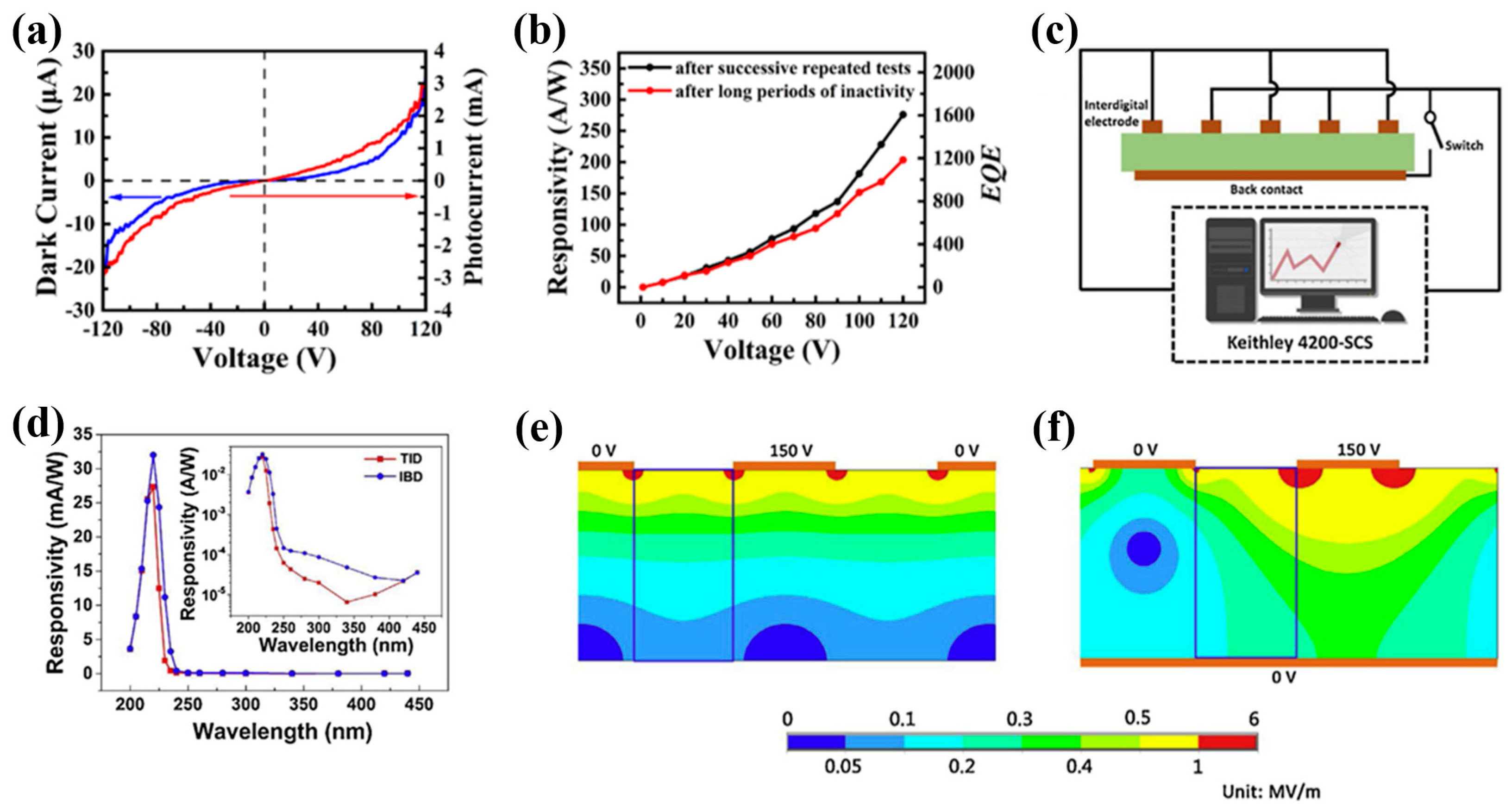
- Li, D.; Gao, W.; Sun, X.; Yu, H.; Liu, C.; Yin, H. Direct Growth of Hexagonal Boron Nitride Thick Films on Dielectric Substrates by Ion Beam Assisted Deposition for Deep-UV Photodetectors. Adv. Opt. Mater. 2021, 9, 2100342. [Google Scholar] [CrossRef]
- Zhang, N.; Song, Y.; Zhou, K.; Wang, W. Enhanced performance of solar-blind photodetector of hexagonal boron nitride with bottom-contact electrodes. AIP Adv. 2020, 10, 085013. [Google Scholar] [CrossRef]
- Zheng, W.; Lin, R.; Zhang, Z.; Huang, F. Vacuum-Ultraviolet Photodetection in Few-Layered h-BN. ACS Appl. Mater. Interfaces 2018, 10, 27116–27123. [Google Scholar] [CrossRef]
- Chen, X.; Tan, C.; Liu, X.; Luan, K.; Guan, Y.; Liu, X.; Zhao, J.; Hou, L.; Gao, Y.; Chen, Z. Growth of hexagonal boron nitride films on silicon substrates by low-pressure chemical vapor deposition. J. Mater. Sci. Mater. Electron. 2021, 32, 3713–3719. [Google Scholar] [CrossRef]
- Feng, Y.; Zhang, Y.; Liu, J.; Zhang, Y.; Xie, Y. Large-Scale Synthesis h-BN Films on Copper-Nickel Alloy by Atmospheric Pressure Chemical Vapor Deposition. Crystals 2022, 12, 985. [Google Scholar] [CrossRef]
- Tan, B.; Yang, H.; Hu, Y.; Gao, F.; Wang, L.; Dai, M.; Zhang, S.; Shang, H.; Chen, H.; Hu, P. Synthesis of High-Quality Multilayer Hexagonal Boron Nitride Films on Au Foils for Ultrahigh Rejection Ratio Solar-Blind Photodetection. ACS Appl. Mater. Interfaces 2020, 12, 28351–28359. [Google Scholar] [CrossRef] [PubMed]
- Yang, H.; Wang, L.; Gao, F.; Dai, M.; Hu, Y.; Chen, H.; Zhang, J.; Qiu, Y.; Jia, D.C.; Zhou, Y.; et al. Shape evolution of two dimensional hexagonal boron nitride single domains on Cu/Ni alloy and its applications in ultraviolet detection. Nanotechnology 2019, 30, 245706. [Google Scholar] [CrossRef]
- Li, J.; Majety, S.; Dahal, R.; Zhao, W.P.; Lin, J.Y.; Jiang, H.X. Dielectric strength, optical absorption, and deep ultraviolet detectors of hexagonal boron nitride epilayers. Appl. Phys. Lett. 2012, 101, 171112. [Google Scholar] [CrossRef] [Green Version]
- Li, X.; Jordan, M.B.; Ayari, T.; Sundaram, S.; El Gmili, Y.; Alam, S.; Alam, M.; Patriarche, G.; Voss, P.L.; Salvestrini, J.P.; et al. Flexible metal-semiconductor-metal device prototype on wafer-scale thick boron nitride layers grown by MOVPE. Sci. Rep. 2017, 7, 786. [Google Scholar] [CrossRef] [Green Version]
- Prakash, A.; Nehate, S.D.; Sundaram, K.B. Boron carbon nitride based metal-insulator-metal UV detectors for harsh environment applications. Opt. Lett. 2016, 41, 4249–4252. [Google Scholar] [CrossRef] [PubMed]
- Jang, A.-R.; Hong, S.; Hyun, C.; Yoon, S.I.; Kim, G.; Jeong, H.Y.; Shin, T.J.; Park, S.O.; Wong, K.W.; Kwak, S.K.; et al. Wafer-Scale and Wrinkle-Free Epitaxial Growth of Single-Orientated Multilayer Hexagonal Boron Nitride on Sapphire. Nano Lett. 2016, 16, 3360–3366. [Google Scholar] [CrossRef]
- Veeralingam, S.; Durai, L.; Yadav, P.; Badhulika, S. Record-High Responsivity and Detectivity of a Flexible Deep-Ultraviolet Photodetector Based on Solid State-Assisted Synthesized hBN Nanosheets. ACS Appl. Electron. Mater. 2021, 3, 1162–1169. [Google Scholar] [CrossRef]
- Garimella, S.V.; Fleischer, A.S.; Murthy, J.Y.; Keshavarzi, A.; Prasher, R.; Patel, C.; Bhavnani, S.H.; Venkatasubramanian, R.; Mahajan, R.; Joshi, Y.; et al. Thermal Challenges in Next-Generation Electronic Systems. IEEE Trans. Compon. Packag. Technol. 2008, 31, 801–815. [Google Scholar] [CrossRef]
- Lin, C.-H.; Fu, H.-C.; Cheng, B.; Tsai, M.-L.; Luo, W.; Zhou, L.; Jang, S.-H.; Hu, L.; He, J.-H. A flexible solar-blind 2D boron nitride nanopaper-based photodetector with high thermal resistance. Npj 2D Mater. Appl. 2018, 2, 23. [Google Scholar] [CrossRef]
- Zhang, W.; Bello, I.; Lifshitz, Y.; Lee, S.T. Recent Advances in Cubic Boron Nitride Deposition. MRS Bull. 2003, 28, 184–188. [Google Scholar] [CrossRef]
- Zhang, W.J.; Chong, Y.M.; Bello, I.; Lee, S.T. Nucleation, growth and characterization of cubic boron nitride (cBN) films. J. Phys. D Appl. Phys. 2007, 40, 6159–6174. [Google Scholar] [CrossRef]
- Soltani, A.; Barkad, H.A.; Mattalah, M.; Benbakhti, B.; De Jaeger, J.-C.; Chong, Y.M.; Zou, Y.S.; Zhang, W.J.; Lee, S.T.; BenMoussa, A.; et al. 193nm deep-ultraviolet solar-blind cubic boron nitride based photodetectors. Appl. Phys. Lett. 2008, 92, 053501. [Google Scholar] [CrossRef]
- Mballo, A.; Srivastava, A.; Sundaram, S.; Vuong, P.; Karrakchou, S.; Halfaya, Y.; Gautier, S.; Voss, P.L.; Ahaitouf, A.; Salvestrini, J.P.; et al. Towards P-Type Conduction in Hexagonal Boron Nitride: Doping Study and Electrical Measurements Analysis of hBN/AlGaN Heterojunctions. Nanomaterials 2021, 11, 211. [Google Scholar] [CrossRef]
- Briegleb, F.; Geuther, A. Ueber das Stickstoffmagnesium und die Affinitäten des Stickgases zu Metallen. Eur. J. Org. Chem. 1862, 123, 228–241. [Google Scholar] [CrossRef] [Green Version]
- Taylor, K.M.; Lenie, C. Some Properties of Aluminum Nitride. J. Electrochem. Soc. 1960, 107, 308. [Google Scholar] [CrossRef]
- Cox, G.; Cummins, D.; Kawabe, K.; Tredgold, R. On the preparation, optical properties and electrical behaviour of aluminium nitride. J. Phys. Chem. Solids 1967, 28, 543–548. [Google Scholar] [CrossRef]
- Alaie, Z.; Nejad, S.M.; Yousefi, M. Recent advances in ultraviolet photodetectors. Mater. Sci. Semicond. Process. 2015, 29, 16–55. [Google Scholar] [CrossRef]
- Liu, F.; Li, L.; Guo, T.; Gan, H.; Mo, X.; Chen, J.; Deng, S.; Xu, N. Investigation on the photoconductive behaviors of an individual AlN nanowire under different excited lights. Nanoscale Res. Lett. 2012, 7, 454. [Google Scholar] [CrossRef] [Green Version]
- Kenry; Yong, K.T.; Yu, S.F. AlN nanowires: Synthesis, physical properties, and nanoelectronics applications. J. Mater. Sci. 2012, 47, 5341–5360. [Google Scholar] [CrossRef]
- Teker, K. Dielectrophoretic Assembly of Aluminum Nitride (AlN) Single Nanowire Deep Ultraviolet Photodetector. J. Nano Res. 2019, 60, 86–93. [Google Scholar] [CrossRef]
- Zheng, W.; Huang, F.; Zheng, R.; Wu, H. Low-Dimensional Structure Vacuum-Ultraviolet-Sensitive (λ < 200 nm) Photodetector with Fast-Response Speed Based on High-Quality AlN Micro/Nanowire. Adv. Mater. 2015, 27, 3921–3927. [Google Scholar]
- Ali, Y.A.; Teker, K. Fabrication of ultraviolet photodetector with aluminum nitride nanowire networks via direct transfer method. Microelectron. Eng. 2019, 211, 26–28. [Google Scholar] [CrossRef]
- Ozdemir, Y.B.; Teker, K.; Yildirim, M.A. High-responsivity flexible ultraviolet photodetector via single aluminum nitride nanowire. Opt. Eng. 2021, 60, 057104. [Google Scholar] [CrossRef]
- Hartmann, C.; Wollweber, J.; Dittmar, A.; Irmscher, K.; Kwasniewski, A.; Langhans, F.; Neugut, T.; Bickermann, M. Preparation of Bulk AlN Seeds by Spontaneous Nucleation of Freestanding Crystals. Jpn. J. Appl. Phys. 2013, 52, 08JA06. [Google Scholar] [CrossRef]
- Wang, Q.; Lei, D.; He, G.; Gong, J.; Huang, J.; Wu, J. Characterization of 60 mm AlN Single Crystal Wafers Grown by the Physical Vapor Transport Method. Phys. Status Solidi 2019, 216, 1900118. [Google Scholar] [CrossRef]
- Hu, W.; Guo, L.; Guo, Y.; Wang, W. Growing AlN crystals on SiC seeds: Effects of growth temperature and seed orientation. J. Cryst. Growth 2020, 541, 125654. [Google Scholar] [CrossRef]
- Knauer, A.; Mogilatenko, A.; Hagedorn, S.; Enslin, J.; Wernicke, T.; Kneissl, M.; Weyers, M. Correlation of sapphire off-cut and reduction of defect density in MOVPE grown AlN. Phys. Status Solidi 2016, 253, 809–813. [Google Scholar] [CrossRef]
- Claudel, A.; Blanquet, E.; Chaussende, D.; Audier, M.; Pique, D.; Pons, M. Thermodynamic and experimental investigations on the growth of thick aluminum nitride layers by high temperature CVD. J. Cryst. Growth 2009, 311, 3371–3379. [Google Scholar] [CrossRef]
- Kumagai, Y.; Kubota, Y.; Nagashima, T.; Kinoshita, T.; Dalmau, R.; Schlesser, R.; Moody, B.; Xie, J.; Murakami, H.; Koukitu, A.; et al. Preparation of a Freestanding AlN Substrate from a Thick AlN Layer Grown by Hydride Vapor Phase Epitaxy on a Bulk AlN Substrate Prepared by Physical Vapor Transport. Appl. Phys. Express 2012, 5, 055504. [Google Scholar] [CrossRef]
- Mansurov, V.; Nikitin, A.; Galitsyn, Y.; Svitasheva, S.; Zhuravlev, K.; Osvath, Z.; Dobos, L.; Horvath, Z.; Pecz, B. AlN growth on sapphire substrate by ammonia MBE. J. Cryst. Growth 2007, 300, 145–150. [Google Scholar] [CrossRef]
- Shukla, G.; Khare, A. Dependence of N2 pressure on the crystal structure and surface quality of AlN thin films deposited via pulsed laser deposition technique at room temperature. Appl. Surf. Sci. 2008, 255, 2057–2062. [Google Scholar] [CrossRef]
- Szekeres, A.; Fogarassy, Z.; Petrik, P.; Vlaikova, E.; Cziraki, A.; Socol, G.; Ristoscu, C.; Grigorescu, S.; Mihailescu, I. Structural characterization of AlN films synthesized by pulsed laser deposition. Appl. Surf. Sci. 2011, 257, 5370–5374. [Google Scholar] [CrossRef]
- Li, T.; Han, J.; Xing, Y.; Deng, X.; Li, J.; Zhang, L.; Shi, F.; Yu, L.; Sun, C.; Zhang, X.; et al. Influence of pressure on the properties of AlN deposited by DC reactive magnetron sputtering on Si (100) substrate. Micro Nano Lett. 2019, 14, 146–149. [Google Scholar] [CrossRef]
- Xiao, S.; Suzuki, R.; Miyake, H.; Harada, S.; Ujihara, T. Improvement mechanism of sputtered AlN films by high-temperature annealing. J. Cryst. Growth 2018, 502, 41–44. [Google Scholar] [CrossRef]
- Chen, M.-R.; Chen, H.-G.; Kao, H.-L.; Wu, M.-G.; Tzou, A.-J.; Chen, J.S.; Chou, H. Structural and optical properties of low temperature grown AlN films on sapphire using helicon sputtering system. J. Vac. Sci. Technol. A 2015, 33, 031503. [Google Scholar] [CrossRef]
- Murtaza, S.H.; Ahmed, S.; Ali, M. Investigation of AlN/Si based heterogeneous Junction using inter-digitated electrodes for enhanced UV light detection. Optik 2022, 265, 169534. [Google Scholar] [CrossRef]
- Yang, R.Y.; Hsiung, C.M.; Chen, H.H.; Wu, H.W.; Shih, M.C. Effect of AlN film thickness on photo/dark currents of MSM UV photodetector. Microw. Opt. Technol. Lett. 2008, 50, 2863–2866. [Google Scholar] [CrossRef]
- Li, T.; Song, W.; Zhang, L.; Yan, J.; Zhu, W.; Wang, L. Self-powered asymmetric metal–semiconductor–metal AlN deep ultraviolet detector. Opt. Lett. 2022, 47, 637–640. [Google Scholar] [CrossRef]
- Li, T.; Long, L.; Hu, Z.; Wan, R.; Gong, X.; Zhang, L.; Yuan, Y.; Yan, J.; Zhu, W.; Wang, L.; et al. Three-dimensional metal–semiconductor–metal AlN deep-ultraviolet detector. Opt. Lett. 2020, 45, 3325–3328. [Google Scholar] [CrossRef]
- Kaushik, S.; Naik, T.R.; Alka, A.; Garg, M.; Tak, B.R.; Ravikanth, M.; Rao, V.R.; Singh, R. Surface Modification of AlN Using Organic Molecular Layer for Improved Deep UV Photodetector Performance. ACS Appl. Electron. Mater. 2020, 2, 739–746. [Google Scholar] [CrossRef]
- Eller, B.S.; Yang, J.; Nemanich, R.J. Electronic surface and dielectric interface states on GaN and AlGaN. J. Vac. Sci. Technol. A 2013, 31, 050807. [Google Scholar] [CrossRef]
- Averin, S.V.; Kuznetsov, P.I.; Zhitov, V.A.; Alkeev, N.V.; Kotov, V.M.; Dorofeev, A.A.; Gladysheva, N.B. AlN/AlGaN heterostructures for selective ultraviolet MSM detectors. Tech. Phys. 2011, 56, 295–297. [Google Scholar] [CrossRef]
- Lu, J.; Lv, Z.; Qiu, X.; Lai, S.; Jiang, H. Ultrasensitive and high-speed AlGaN/AlN solar-blind ultraviolet photodetector: A full-channel-self-depleted phototransistor by a virtual photogate. Photon Res. 2022, 10, 2229. [Google Scholar] [CrossRef]
- Hao, Y.; Wang, X.; An, Y. A Ga2O3/AlN heterojunction for self-powered solar-blind photodetection with high photo-to-dark current ratio and fast response speed. Phys. Scr. 2021, 96, 125835. [Google Scholar] [CrossRef]
- Li, T.; Lu, Y.; Chen, Z. Heteroepitaxy Growth and Characterization of High-Quality AlN Films for Far-Ultraviolet Photodetection. Nanomaterials 2022, 12, 4169. [Google Scholar] [CrossRef]
- Cai, Q.; You, H.; Guo, H.; Wang, J.; Liu, B.; Xie, Z.; Chen, D.; Lu, H.; Zheng, Y.; Zhang, R. Progress on AlGaN-based solar-blind ultraviolet photodetectors and focal plane arrays. Light Sci. Appl. 2021, 10, 94. [Google Scholar] [CrossRef]
- Li, D.B.; Jiang, K.; Sun, X.J.; Guo, C.L. AlGaN photonics: Recent advances in materials and ultraviolet devices. Adv. Opt. Photonics 2018, 10, 43–110. [Google Scholar] [CrossRef]
- Su, L.; Yang, W.; Cai, J.; Chen, H.; Fang, X. Self-Powered Ultraviolet Photodetectors Driven by Built-In Electric Field. Small 2017, 13, 1701687. [Google Scholar] [CrossRef] [PubMed] [Green Version]
- Tian, W.; Wang, Y.; Chen, L.; Li, L. Self-Powered Nanoscale Photodetectors. Small 2017, 13, 1701848. [Google Scholar] [CrossRef] [Green Version]
- Wang, D.; Huang, C.; Liu, X.; Zhang, H.; Yu, H.; Fang, S.; Ooi, B.S.; Mi, Z.; He, J.H.; Sun, H. Highly Uniform, Self-Assembled AlGaN Nanowires for Self-Powered Solar-Blind Photodetector with Fast-Response Speed and High Responsivity. Adv. Opt. Mater. 2021, 9, 2000893. [Google Scholar] [CrossRef]
- Kang, S.; Chatterjee, U.; Um, D.Y.; Yu, Y.T.; Seo, I.S.; Lee, C.R. Ultraviolet-C Photodetector Fabricated Using Si-Doped n-AlGaN Nanorods Grown by MOCVD. ACS Photonics 2017, 4, 2595–2603. [Google Scholar] [CrossRef]
- Ouyang, W.; Teng, F.; He, J.; Fang, X. Enhancing the Photoelectric Performance of Photodetectors Based on Metal Oxide Semiconductors by Charge-Carrier Engineering. Adv. Funct. Mater. 2019, 29, 1807672. [Google Scholar] [CrossRef]
- Lu, N.; Gu, Y.; Weng, Y.; Dai, Z.; Ding, Y. Localized surface plasmon enhanced photoresponse of AlGaN MSM solar-blind ultraviolet photodetectors. Mater. Res. Express 2019, 6, 095033. [Google Scholar] [CrossRef]
- Jia, C.; Li, X.; Xin, N.; Gong, Y.; Guan, J.; Meng, L.; Meng, S.; Guo, X. Interface-Engineered Plasmonics in Metal/Semiconductor Heterostructures. Adv. Energy Mater. 2016, 6, 1600431. [Google Scholar] [CrossRef]
- Wu, Y.; Sun, X.; Shi, Z.; Jia, Y.; Jiang, K.; Ben, J.; Kai, C.; Wang, Y.; Lü, W.; Li, D. In situ fabrication of Al surface plasmon nanoparticles by metal-organic chemical vapor deposition for enhanced performance of AlGaN deep ultraviolet detectors. Nanoscale Adv. 2020, 2, 1854–1858. [Google Scholar] [CrossRef] [Green Version]
- Rathkanthiwar, S.; Kalra, A.; Muralidharan, R.; Nath, D.N.; Raghavan, S. V-Pits-Induced Photoresponse Enhancement in AlGaN UV-B Photodetectors on Si (111). IEEE Trans. Electron Devices 2020, 67, 4281–4287. [Google Scholar] [CrossRef]
- Zhao, Y.; Donaldson, W.R. Ultrafast UV AlGaN Metal–Semiconductor–Metal Photodetector With a Response Time Below 25 ps. IEEE J. Quantum Electron. 2020, 56, 1–7. [Google Scholar] [CrossRef]
- Chen, Y.; Zang, H.; Ben, J.; Zhang, S.; Jiang, K.; Shi, Z.; Jia, Y.; Liu, M.; Sun, X.; Li, D. AlGaN UV Detector with Largely Enhanced Heat Dissipation on Mo Substrate Enabled by van der Waals Epitaxy. Cryst. Growth Des. 2023, 23, 1162–1171. [Google Scholar] [CrossRef]
- Kalra, A.; Rathkanthiwar, S.; Muralidharan, R.; Raghavan, S.; Nath, D.N. Polarization-Graded AlGaN Solar-Blind p-i-n Detector With 92% Zero-Bias External Quantum Efficiency. IEEE Photonics Technol. Lett. 2019, 31, 1237–1240. [Google Scholar] [CrossRef]
- Kalra, A.; Rathkanthiwar, S.; Muralidharan, R.; Raghavan, S.; Nath, D.N. Material-to-device performance correlation for AlGaN-based solar-blind p-i-n photodiodes. Semicond. Sci. Technol. 2020, 35, 035001. [Google Scholar] [CrossRef]
- Kurose, N.; Iwata, N.; Kamiya, I.; Aoyagi, Y. Formation of conductive spontaneous via holes in AlN buffer layer on n(+)Si substrate by filling the vias with n-AlGaN by metal organic chemical vapor deposition and application to vertical deep ultraviolet photo-sensor. AIP Adv. 2014, 4, 123007. [Google Scholar] [CrossRef] [Green Version]
- Gautam, L.; Lee, J.; Brown, G.; Razeghi, M. Low Dark Current Deep UV AlGaN Photodetectors on AlN Substrate. IEEE J. Quantum Electron. 2022, 58, 1–5. [Google Scholar] [CrossRef]
- Zhou, M.; Qiu, H.; He, T.; Zhang, J.; Yang, W.; Lu, S.; Bian, L.; Zhao, Y. UV Photodetector Based on Vertical (Al, Ga)N Nanowires with Graphene Electrode and Si Substrate. Phys. Status Solidi 2020, 217, 2000061. [Google Scholar] [CrossRef]
- Rodak, L.E.; Sampath, A.V.; Gallinat, C.S.; Enck, R.W.; Smith, J.; Shen, H.; Wraback, M.; Chen, Y.; Zhou, Q.; Campbell, J.C. Aluminum gallium nitride/silicon carbide separate absorption and multiplication avalanche photodiodes. In Proceedings of the 2012 Lester Eastman Conference on High Performance Devices, Providence, RI, USA, 7–9 August 2012. [Google Scholar]
- Sood, A.K.; Zeller, J.W.; Ghuman, P.; Babu, S.; Dupuis, R.D. GaN/AlGaN avalanche photodiode detector technology for high performance ultraviolet sensing applications. In Proceedings of the SPIE—The International Society for Optical Engineering, Online, 24 August–4 September 2020. [Google Scholar]
- Nguyen, H.Q.; Foisal, A.R.; Nguyen, T.; Nguyen, H.; Vu, T.H.; Fastier-Wooller, J.; Aberoumand, S.; Phan, H.P.; Dao, D.V. Rapid Fabrication of High-responsivity Photodetectors Utilizing AlGaN/GaN on Sapphire. In Proceedings of the IEEE Sensors, Sydney, Australia, 31 October–3 November 2021. [Google Scholar]
- Gao, J.; Li, Y.; Hu, Y.; Wang, Z.; Hu, A.; Guo, X. A 2DEG back-gated graphene/AlGaN deep-ultraviolet photodetector with ultrahigh responsivity. Chin. Phys. B 2020, 29, 128502. [Google Scholar] [CrossRef]
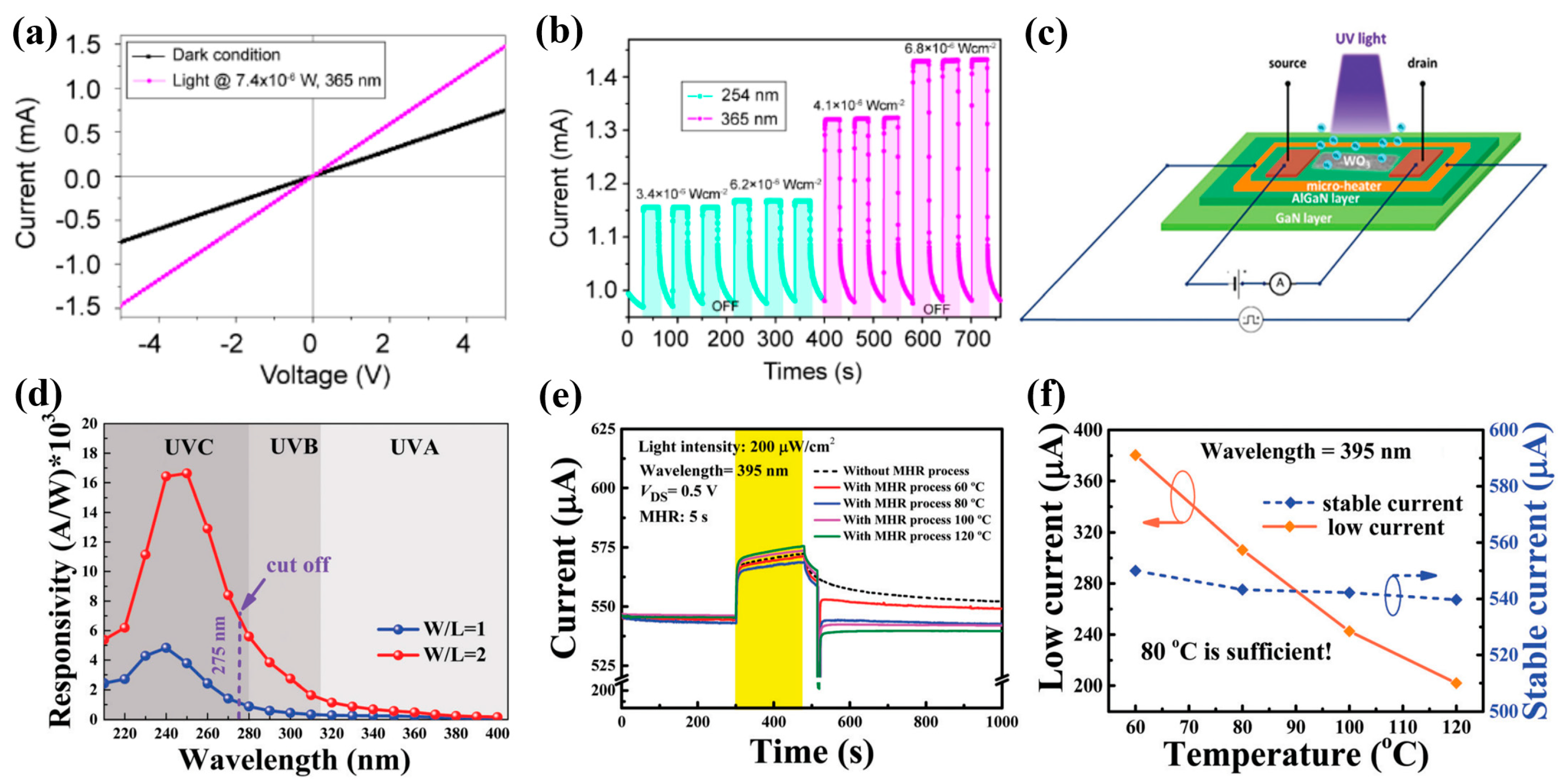
- Sun, J.; Zhan, T.; Liu, Z.; Wang, J.; Yi, X.; Sarro, P.M.; Zhang, G. Suspended tungsten trioxide (WO3) gate AlGaN/GaN heterostructure deep ultraviolet detectors with integrated micro-heater. Opt. Express 2019, 27, 36405–36413. [Google Scholar] [CrossRef] [Green Version]
- Sun, J.; Zhang, S.; Zhan, T.; Liu, Z.; Wang, J.; Yi, X.; Li, J.; Sarro, P.M.; Zhang, G. A high responsivity and controllable recovery ultraviolet detector based on a WO3 gate AlGaN/GaN heterostructure with an integrated micro-heater. J. Mater. Chem. C 2020, 8, 5409–5416. [Google Scholar] [CrossRef]
- Cicek, E.; McClintock, R.; Cho, C.Y.; Rahnema, B.; Razeghi, M. AlxGa1-xN-based back-illuminated solar-blind photodetectors with external quantum efficiency of 89%. Appl. Phys. Lett. 2013, 103, 191108. [Google Scholar] [CrossRef]
- Higashiwaki, M.; Sasaki, K.; Kuramata, A.; Masui, T.; Yamakoshi, S. Gallium oxide (Ga2O3) metal-semiconductor field-effect transistors on single-crystal β-Ga2O3 (010) substrates. Appl. Phys. Lett. 2012, 100, 013504. [Google Scholar] [CrossRef]
- El-Sayed, E.I.; Al-Ghamdi, A.A.; Al-Heniti, S.; Al-Marzouki, F.; El-Tantawy, F. Synthesis of ultrafine β-Ga2O3 nanopowder via hydrothermal approach: A strong UV “excimer-like” emission. Mater. Lett. 2011, 65, 317–321. [Google Scholar] [CrossRef]
- Ruan, M.M.; Yang, Z.; Teng, Y.; Wang, Q.S.; Wang, Y.Q. Novel green synthesis and improved solar-blind detection performance of hierarchical γ-Ga2O3 nanospheres. J. Mater. Chem. C 2017, 5, 7161–7166. [Google Scholar] [CrossRef]
- Rafique, S.; Karim, M.R.; Johnson, J.M.; Hwang, J.; Zhao, H. LPCVD homoepitaxy of Si doped β-Ga2O3 thin films on (010) and (001) substrates. Appl. Phys. Lett. 2018, 112, 052104. [Google Scholar] [CrossRef] [Green Version]
- Weng, W.Y.; Hsueh, T.J.; Chang, S.J.; Huang, G.J.; Chang, S.P. A Solar-Blind β-Ga2O3 Nanowire Photodetector. IEEE Photonics Technol. Lett. 2010, 22, 709–711. [Google Scholar] [CrossRef]
- Wu, Y.L.; Chang, S.J.; Weng, W.Y.; Liu, C.H.; Tsai, T.Y.; Hsu, C.L.; Chen, K.C. Ga2O3 Nanowire Photodetector Prepared on SiO2/Si Template. IEEE Sens. J. 2013, 13, 2368–2373. [Google Scholar] [CrossRef]
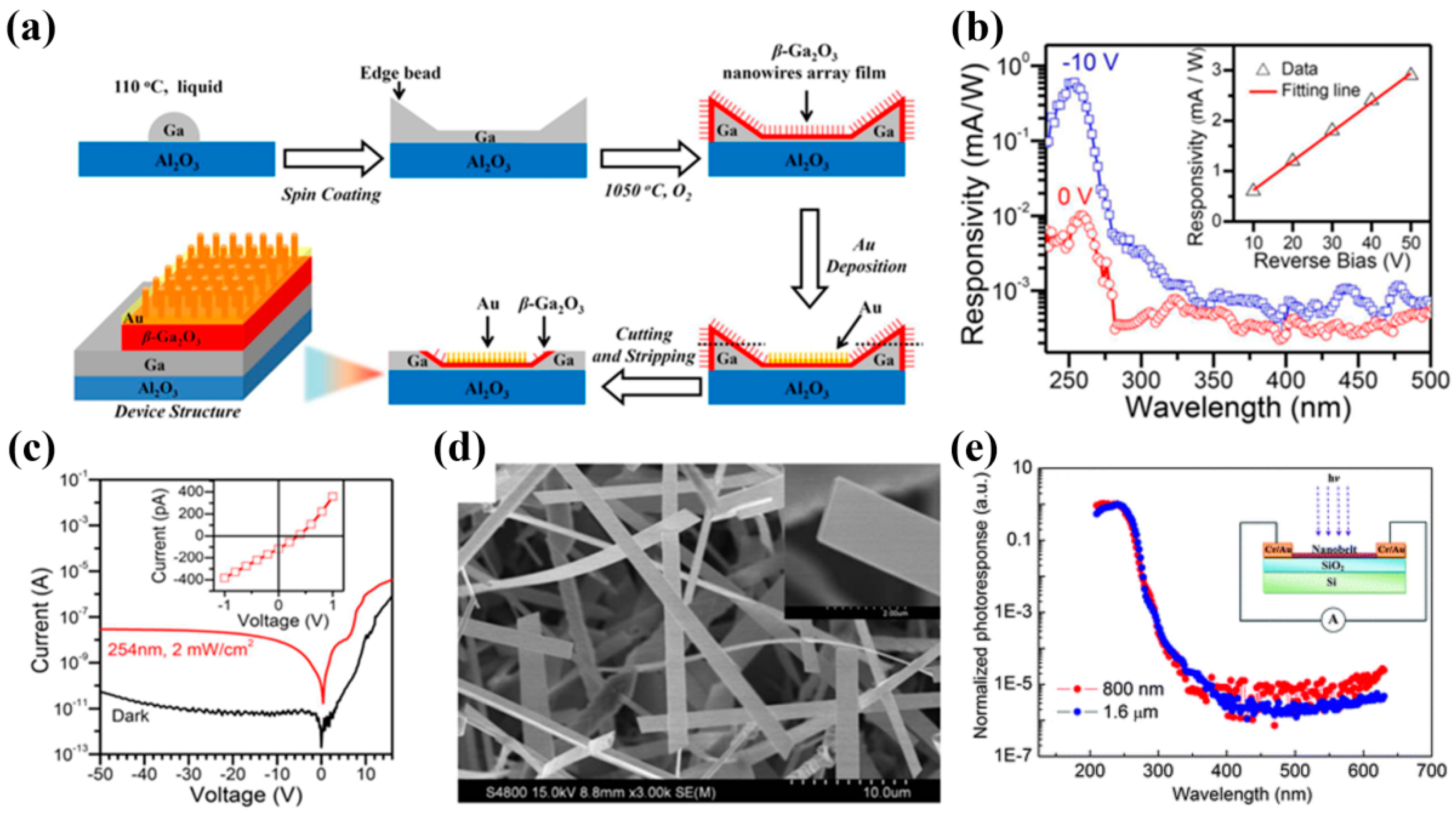
- Chen, X.; Liu, K.; Zhang, Z.; Wang, C.; Li, B.; Zhao, H.; Zhao, D.; Shen, D. Self-Powered Solar-Blind Photodetector with Fast Response Based on Au/β-Ga2O3 Nanowires Array Film Schottky Junction. ACS Appl. Mater. Interfaces 2016, 8, 4185–4191. [Google Scholar] [CrossRef] [PubMed]
- Du, J.; Xing, J.; Ge, C.; Liu, H.; Liu, P.; Hao, H.; Dong, J.; Zheng, Z.; Gao, H. Highly sensitive and ultrafast deep UV photodetector based on a beta-Ga2O3 nanowire network grown by CVD. J. Phys. D-Appl. Phys. 2016, 49, 425105. [Google Scholar] [CrossRef]
- Li, L.; Auer, E.; Liao, M.; Fang, X.; Zhai, T.; Gautam, U.K.; Lugstein, A.; Koide, Y.; Bando, Y.; Golberg, D. Deep-ultraviolet solar-blind photoconductivity of individual gallium oxide nanobelts. Nanoscale 2011, 3, 1120–1126. [Google Scholar] [CrossRef]
- Zhong, M.; Wei, Z.; Meng, X.; Wu, F.; Li, J. High-performance single crystalline UV photodetectors of β-Ga2O3. J. Alloys Compd. 2015, 619, 572–575. [Google Scholar] [CrossRef]
- Teng, Y.; Song, L.X.; Ponchel, A.; Yang, Z.K.; Xia, J. Self-Assembled Metastable γ-Ga2O3 Nanoflowers with Hexagonal Nanopetals for Solar-Blind Photodetection. Adv. Mater. 2014, 26, 6238–6243. [Google Scholar] [CrossRef]
- Feng, W.; Wang, X.; Zhang, J.; Wang, L.; Zheng, W.; Hu, P.; Cao, W.; Yang, B. Synthesis of two-dimensional β-Ga2O3 nanosheets for high-performance solar blind photodetectors. J. Mater. Chem. C 2014, 2, 3254–3259. [Google Scholar] [CrossRef]
- Oh, S.; Kim, J.; Ren, F.; Pearton, S.J.; Kim, J. Quasi-two-dimensional b-gallium oxide solar-blind photodetectors with ultrahigh responsivity. J. Mater. Chem. C 2016, 4, 9245–9250. [Google Scholar] [CrossRef]
- Oh, S.; Mastro, M.A.; Tadjer, M.J.; Kim, J. Solar-Blind Metal-Semiconductor-Metal Photodetectors Based on an Exfoliated β-Ga2O3 Micro-Flake. ECS J. Solid State Sci. Technol. 2017, 6, Q79. [Google Scholar] [CrossRef]
- Kwon, Y.; Lee, G.; Oh, S.; Kim, J.; Pearton, S.J.; Ren, F. Tuning the thickness of exfoliated quasi-two-dimensional β-Ga2O3 flakes by plasma etching. Appl. Phys. Lett. 2017, 110, 131901. [Google Scholar] [CrossRef] [Green Version]
- Xu, Y.; Chen, X.; Zhou, D.; Ren, F.; Zhou, J.; Bai, S.; Lu, H.; Gu, S.; Zhang, R.; Zheng, Y.; et al. Carrier Transport and Gain Mechanisms in β-Ga2O3-Based Metal-Semiconductor-Metal Solar-Blind Schottky Photodetectors. IEEE Trans. Electron. Devices 2019, 66, 2276–2281. [Google Scholar] [CrossRef]
- Tak, B.R.; Garg, M.; Dewan, S.; Torres-Castanedo, C.G.; Li, K.H.; Gupta, V.; Li, X.; Singh, R. High-temperature photocurrent mechanism of β-Ga2O3 based metal-semiconductor-metal solar-blind photodetectors. J. Appl. Phys. 2019, 125, 144501. [Google Scholar] [CrossRef] [Green Version]
- Tak, B.R.; Yang, M.M.; Alexe, M.; Singh, R. Deep-Level Traps Responsible for Persistent Photocurrent in Pulsed-Laser-Deposited β-Ga2O3 Thin Films. Crystals 2021, 11, 1046. [Google Scholar] [CrossRef]
- Tak, B.R.; Alexe, M.; Singh, R. Investigation of Deep Level Traps Responsible for Persistent Photocurrent in Pulsed Laser Deposited β-Ga2O3 Thin Films. In Proceedings of the 2020 5th IEEE International Conference on Emerging Electronics, Jaipur, India, 1–3 December 2020. [Google Scholar]
- Chu, S.-Y.; Shen, M.-X.; Yeh, T.-H.; Chen, C.-H.; Lee, C.-T.; Lee, H.-Y. Investigation of Ga2O3-Based Deep Ultraviolet Photodetectors Using Plasma-Enhanced Atomic Layer Deposition System. Sensors 2020, 20, 6159. [Google Scholar] [CrossRef]
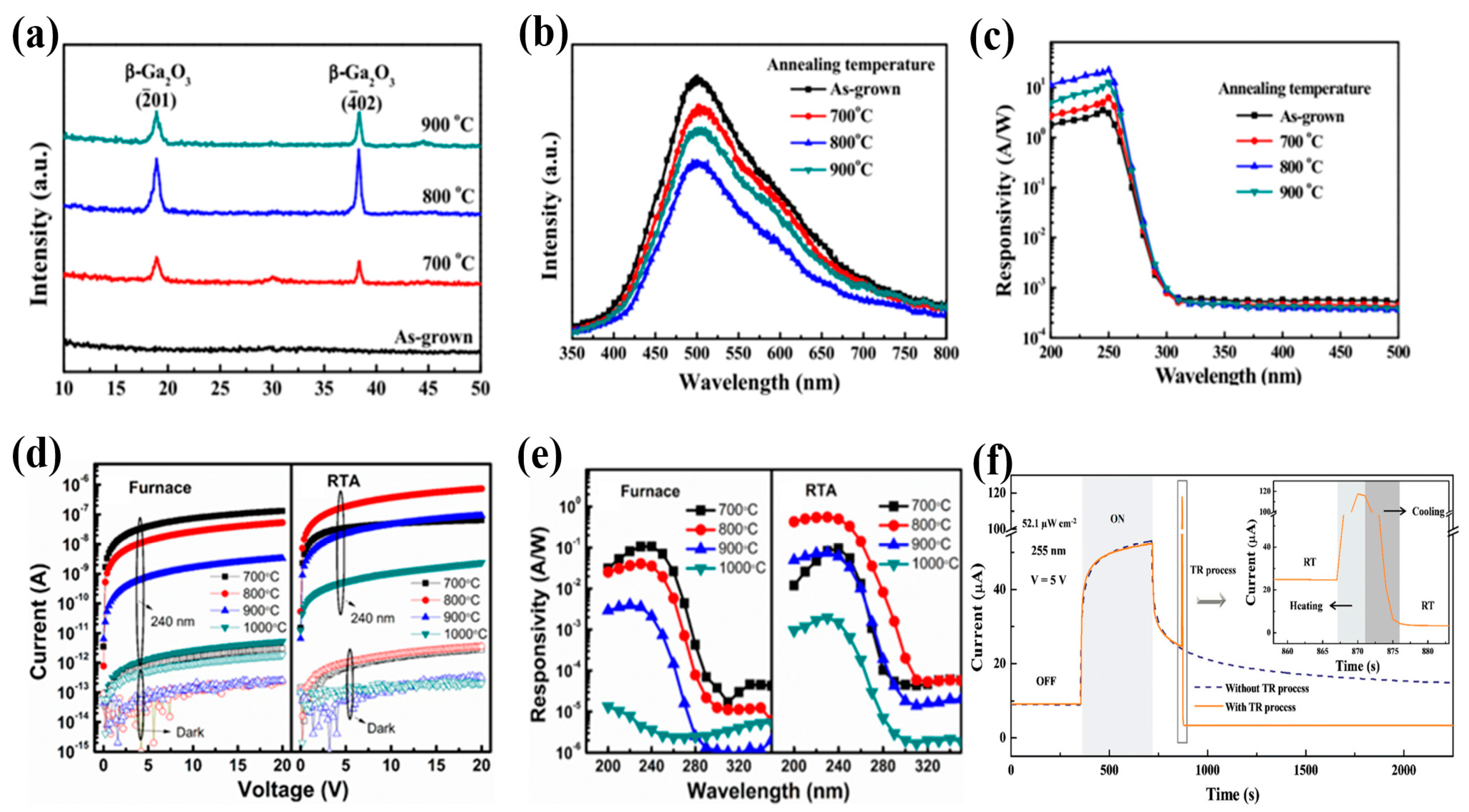
- Li, H.; Chen, P.-W.; Yuan, S.-H.; Huang, T.-M.; Zhang, S.; Wuu, D.-S. Improved Performance of Deep Ultraviolet Photodetector From Sputtered Ga2O3 Films Using Post-Thermal Treatments. IEEE Photonics J. 2019, 11, 1–8. [Google Scholar] [CrossRef]
- Zhou, H.; Cong, L.; Ma, J.; Li, B.; Chen, M.; Xu, H.; Liu, Y. High gain broadband photoconductor based on amorphous Ga2O3 and suppression of persistent photoconductivity. J. Mater. Chem. C 2019, 7, 13149–13155. [Google Scholar] [CrossRef]
- Zhang, T.; Guan, D.; Liu, N.; Zhang, J.; Zhang, J.; Guo, C.; Qiu, M.; Yuan, Q.; Zhang, W.; Ye, J. Room temperature fabrication and post-annealing treatment of amorphous Ga2O3 photodetectors for deep-ultraviolet light detection. Appl. Phys. Express 2022, 15, 022007. [Google Scholar] [CrossRef]
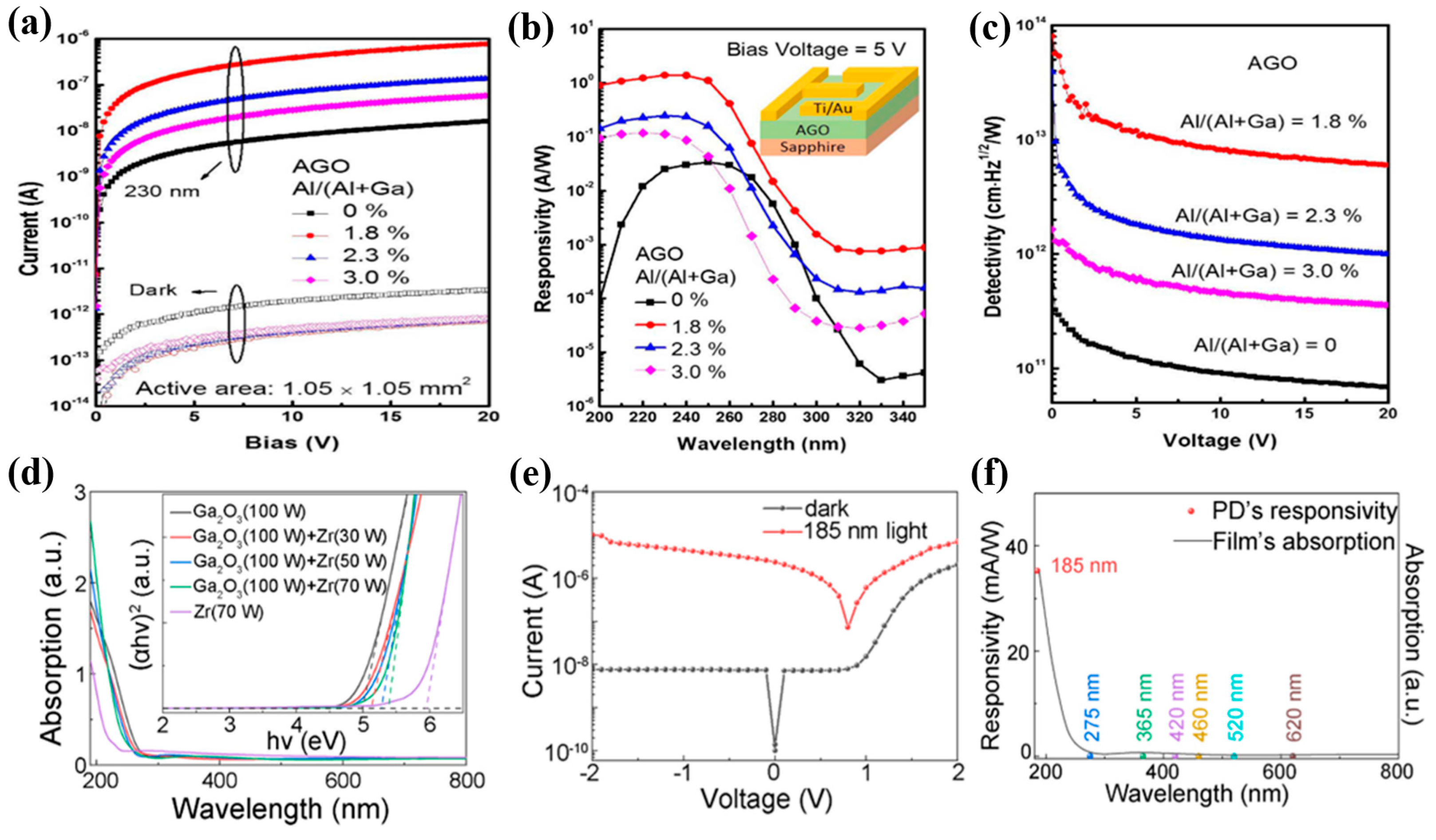
- Yuan, S.-H.; Wang, C.-C.; Huang, S.-Y.; Wuu, D.-S. Improved Responsivity Drop From 250 to 200 nm in Sputtered Gallium Oxide Photodetectors by Incorporating Trace Aluminum. IEEE Electron Device Lett. 2018, 39, 220–223. [Google Scholar] [CrossRef]
- Lee, H.Y.; Liu, J.T.; Lee, C.T. Modulated Al2O3-Alloyed Ga2O3 Materials and Deep Ultraviolet Photodetectors. IEEE Photonics Technol. Lett. 2018, 30, 549–552. [Google Scholar] [CrossRef]
- Chen, P.-W.; Huang, S.-Y.; Wang, C.-C.; Yuan, S.-H.; Wuu, D.-S. Influence of oxygen on sputtering of aluminum-gallium oxide films for deep-ultraviolet detector applications. J. Alloys Compd. 2019, 791, 1213–1219. [Google Scholar] [CrossRef]
- Guo, J.; Ma, M.; Li, Y.; Zhang, D.; Liu, Y.; Zheng, W. Bandgap Engineering of ZrGaO Films for Deep-Ultraviolet Detection. IEEE Electron Device Lett. 2021, 42, 895–898. [Google Scholar] [CrossRef]
- Li, Y.; Li, Y.; Ji, Y.; Wang, H.; Zhong, D. Sol-gel preparation of Sn doped gallium oxide films for application in solar-blind ultraviolet photodetectors. J. Mater. Sci. 2022, 57, 1186–1197. [Google Scholar] [CrossRef]
- Mukhopadhyay, P.; Schoenfeld, W.V. High responsivity tin gallium oxide Schottky ultraviolet photodetectors. J. Vac. Sci. Technol. A 2020, 38, 013403. [Google Scholar] [CrossRef]
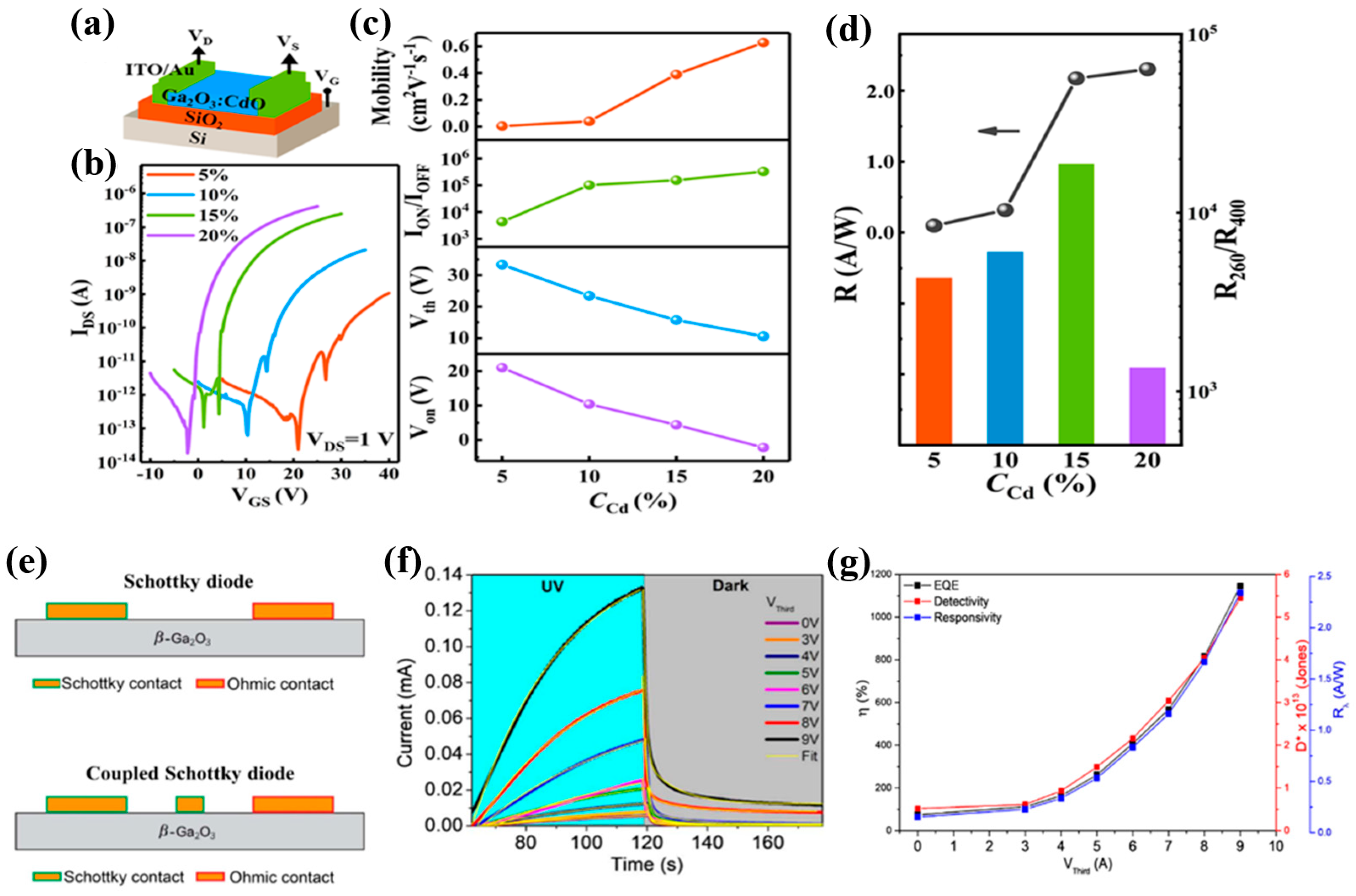
- Xiao, X.; Liang, L.; Pei, Y.; Yu, J.; Duan, H.; Chang, T.C.; Cao, H. Solution-processed amorphous Ga2O3: CdO TFT-type deep-UV photodetectors. Appl. Phys. Lett. 2020, 116, 192102. [Google Scholar] [CrossRef]
- Yu, J.; Javaid, K.; Liang, L.; Wu, W.; Liang, Y.; Song, A.; Zhang, H.; Shi, W.; Chang, T.-C.; Cao, H. High-Performance Visible-Blind Ultraviolet Photodetector Based on IGZO TFT Coupled with p–n Heterojunction. ACS Appl. Mater. Interfaces 2018, 10, 8102–8109. [Google Scholar] [CrossRef]
- Pintor-Monroy, M.I.; Reyes-Banda, M.G.; Avila-Avendano, C.; Quevedo-Lopez, M.A. Tuning Electrical Properties of Amorphous Ga2O3 Thin Films for Deep UV Phototransistors. IEEE Sens. J. 2021, 21, 14807–14814. [Google Scholar] [CrossRef]
- Li, X.X.; Zeng, G.; Li, Y.C.; Yu, Q.J.; Liu, M.Y.; Zhu, L.Y.; Liu, W.; Yang, Y.G.; Zhang, D.W.; Lu, H.L. Highly sensitive and stable β-Ga2O3 DUV phototransistor with local back-gate structure and its neuromorphic application. Nano Res. 2022, 15, 9359–9367. [Google Scholar] [CrossRef]
- Vieira, D.H.; Badiei, N.; Evans, J.E.; Alves, N.; Kettle, J.; Li, L. Improvement of the Deep UV Sensor Performance of a β-Ga2O3 Photodiode by Coupling of Two Planar Diodes. IEEE Trans. Electron. Devices 2020, 67, 4947–4952. [Google Scholar] [CrossRef]
- Mondal, A.; Nandi, S.; Yadav, M.K.; Nandi, A.; Bag, A. Broad Range (254–302 nm) and High Performance Ga2O3: SnO2 Based Deep UV Photodetector. IEEE Trans. Nanotechnol. 2022, 21, 320–327. [Google Scholar] [CrossRef]
- Zhao, B.; Wang, F.; Chen, H.; Wang, Y.; Jiang, M.; Fang, X.; Zhao, D. Solar-Blind Avalanche Photodetector Based On Single ZnO–Ga2O3 Core–Shell Microwire. Nano Lett. 2015, 15, 3988–3993. [Google Scholar] [CrossRef]
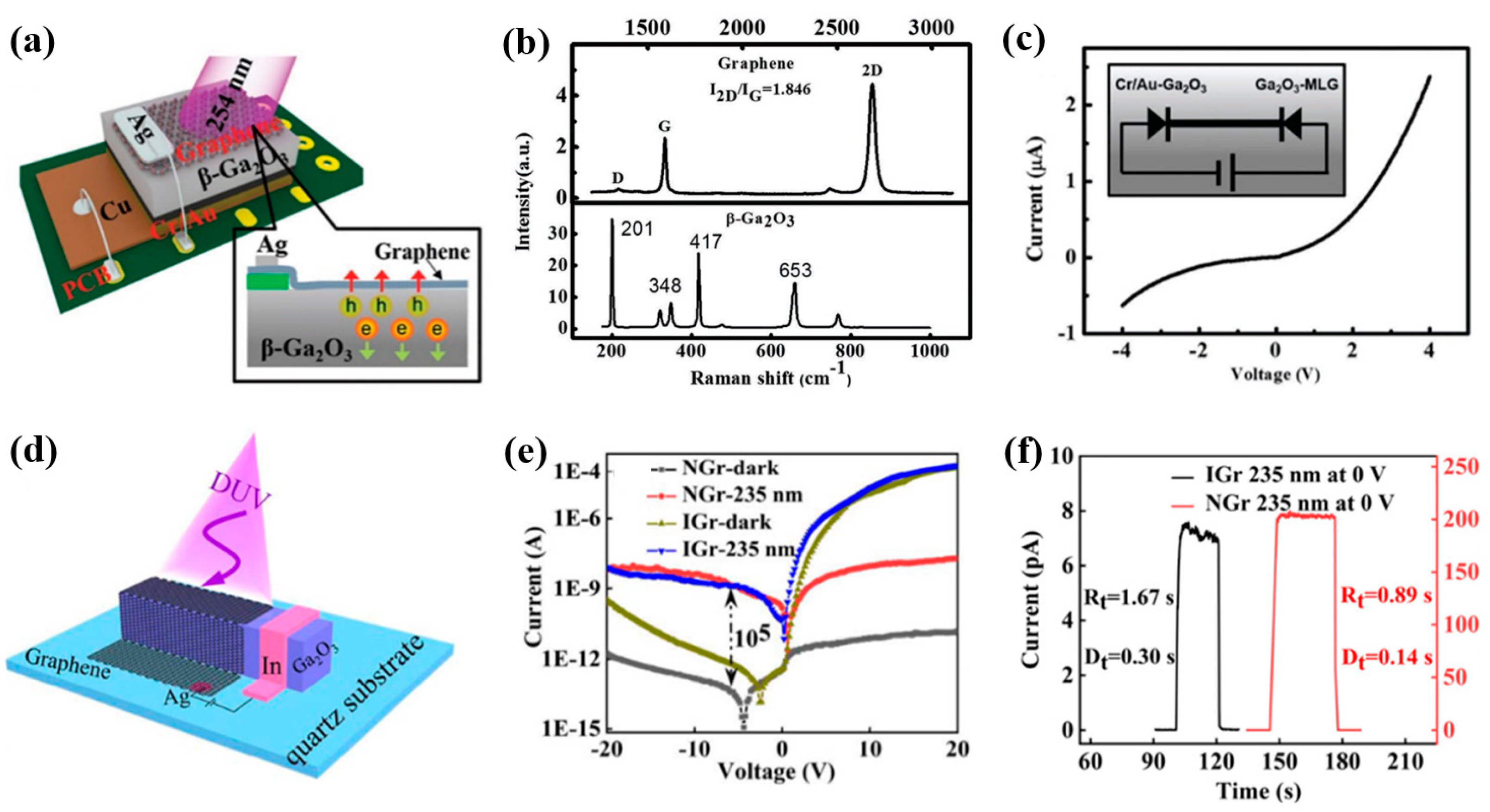
- Kong, W.Y.; Wu, G.A.; Wang, K.Y.; Zhang, T.F.; Zou, Y.F.; Wang, D.D.; Luo, L.B. Graphene-β-Ga2O3 Heterojunction for Highly Sensitive Deep UV Photodetector Application. Adv. Mater. 2016, 28, 10725–10731. [Google Scholar] [CrossRef] [PubMed]
- Wang, Y.; Fu, R.; Wang, Y.; Li, B.; Xu, H.; Shen, A.; Liu, Y. A High Responsivity Self-Powered Solar-Blind DUV Photodetector Based on a Nitrogen-Doped Graphene/β-Ga2O3 Microwire p-n Heterojunction. IEEE Electron Device Lett. 2022, 43, 1073–1076. [Google Scholar] [CrossRef]
- Kumar, A.; Nandi, A.; Bag, A. Exceptional Responsivity (>6 kA/W) and Dark Current (<70 fA) Tradeoff of n-Ga2O3/p-CuO Quasi-Heterojunction-Based Deep UV Photodetector. IEEE Trans. Electron Devices 2021, 68, 144–151. [Google Scholar]
- Li, S.; Yan, Z.Y.; Tang, J.C.; Yue, J.Y.; Liu, Z.; Li, P.G.; Guo, Y.F.; Tang, W.H. Ga2O3/V2O5 Oxide Heterojunction Photovoltaic Photodetector With Superhigh Solar-Blind Spectral Discriminability. IEEE Trans. Electron Devices 2022, 69, 2443–2448. [Google Scholar] [CrossRef]
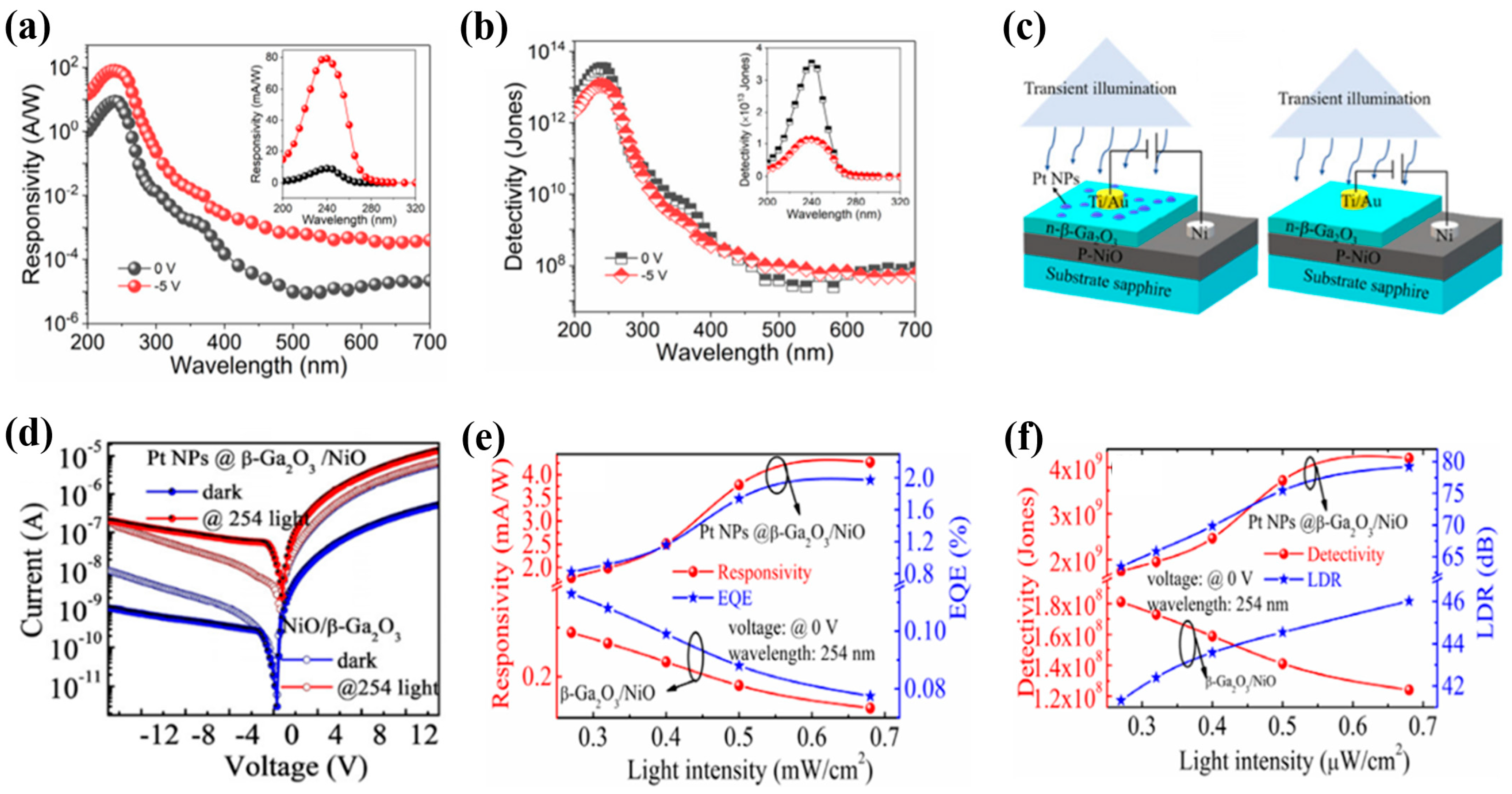
- Yu, J.; Yu, M.; Wang, Z.; Yuan, L.; Huang, Y.; Zhang, L.; Zhang, Y.; Jia, R. Improved Photoresponse Performance of Self-Powered beta-Ga2O3/NiO Heterojunction UV Photodetector by Surface Plasmonic Effect of Pt Nanoparticles. IEEE Trans. Electron Devices 2020, 67, 3199–3204. [Google Scholar] [CrossRef]
- Huang, L.; Hu, Z.; Zhang, H.; Xiong, Y.; Fan, S.; Kong, C.; Li, W.; Ye, L.; Li, H. A simple, repeatable and highly stable self-powered solar-blind photoelectrochemical-type photodetector using amorphous Ga2O3 films grown on 3D carbon fiber paper. J. Mater. Chem. C 2021, 9, 10354–10360. [Google Scholar] [CrossRef]
- Wang, Y.; Li, L.; Wang, H.; Su, L.; Chen, H.; Bian, W.; Ma, J.; Li, B.; Liu, Z.; Shen, A. An ultrahigh responsivity self-powered solar-blind photodetector based on a centimeter-sized β-Ga2O3/polyaniline heterojunction. Nanoscale 2020, 12, 1406–1413. [Google Scholar] [CrossRef]
- Bundy, F.P.; Hall, H.T.; Strong, H.M.; Wentorfjun, R.H. Man-Made Diamonds. Nature 1955, 176, 51–55. [Google Scholar] [CrossRef]
- Derjaguin, B.; Fedoseev, D.; Lukyanovich, V.; Spitzin, B.; Ryabov, V.; Lavrentyev, A. Filamentary diamond crystals. J. Cryst. Growth 1968, 2, 380–384. [Google Scholar] [CrossRef]
- Angus, J.C.; Will, H.A.; Stanko, W.S. Growth of Diamond Seed Crystals by Vapor Deposition. J. Appl. Phys. 1968, 39, 2915–2922. [Google Scholar] [CrossRef]
- Wang, S.F.; Li, D.M.; Xiao, Y.H.; Yang, Z.C.; Li, J.P.; Hao, J. Diamond Radiation Detector Used for Space Radiation Detection: A State-of-Art Review. Mater. Rev. 2018, 32, 1459–1468. [Google Scholar]
- Alvarez, J.; Liao, M.; Koide, Y. Large deep-ultraviolet photocurrent in metal-semiconductor-metal structures fabricated on as-grown boron-doped diamond. Appl. Phys. Lett. 2005, 87, 113507. [Google Scholar] [CrossRef]
- Liao, M.; Koide, Y. High-performance metal-semiconductor-metal deep-ultraviolet photodetectors based on homoepitaxial diamond thin film. Appl. Phys. Lett. 2006, 89, 113509. [Google Scholar] [CrossRef]
- Bevilacqua, M.; Jackman, R.B. Extreme sensitivity displayed by single crystal diamond deep ultraviolet photoconductive devices. Appl. Phys. Lett. 2009, 95, 243501. [Google Scholar] [CrossRef]
- Koide, Y.; Liao, M.; Imura, M. Mechanism of photoconductivity gain and persistent photoconductivity for diamond photodetector. Diam. Relat. Mater. 2010, 19, 205–207. [Google Scholar] [CrossRef]
- Mendoza, F.; Makarov, V.; Weiner, B.R.; Morell, G. Solar-blind field-emission diamond ultraviolet detector. Appl. Phys. Lett. 2015, 107, 201605. [Google Scholar] [CrossRef] [Green Version]
- Feng, M.; Jin, P.; Meng, X.; Xu, P.; Huo, X.; Zhou, G.; Qu, P.; Wu, J.; Wang, Z. Performance of metal-semiconductor-metal structured diamond deep-ultraviolet photodetector with a large active area. J. Phys. D Appl. Phys. 2022, 55, 404005. [Google Scholar] [CrossRef]
- Girolami, M.; Serpente, V.; Mastellone, M.; Tardocchi, M.; Rebai, M.; Xiu, Q.; Liu, J.; Sun, Z.; Zhao, Y.; Valentini, V.; et al. Self-powered solar-blind ultrafast UV-C diamond detectors with asymmetric Schottky contacts. Carbon 2022, 189, 27–36. [Google Scholar] [CrossRef]
- Liao, M.; Alvarez, J.; Imura, M.; Koide, Y. Submicron metal-semiconductor-metal diamond photodiodes toward improving the responsivity. Appl. Phys. Lett. 2007, 91, 163510. [Google Scholar] [CrossRef]
- Liu, K.; Liu, B.; Zhao, J.; Shu, G.; Xu, X.; Yao, K.; Sun, M.; Zhang, X.; Yang, Y.; Su, Z.; et al. Application of back bias to interdigital-electrode structured diamond UV detector showing enhanced responsivity. Sensors Actuators A Phys. 2019, 290, 222–227. [Google Scholar] [CrossRef]
- Wang, S.G.; Sellin, P.J.; Lohstroh, A.; Zhang, Q. Performance improvement of polycrystalline diamond ultraviolet photodetectors by room-temperature plasma treatment. Appl. Phys. Lett. 2005, 86, 093503. [Google Scholar] [CrossRef] [Green Version]
- Liu, Z.; Zhao, D.; Min, T.; Wang, J.; Chen, G.; Wang, H.-X. Photovoltaic Three-Dimensional Diamond UV Photodetector With Low Dark Current and Fast Response Speed Fabricated by Bottom-Up Method. IEEE Electron Device Lett. 2019, 40, 1186–1189. [Google Scholar] [CrossRef]
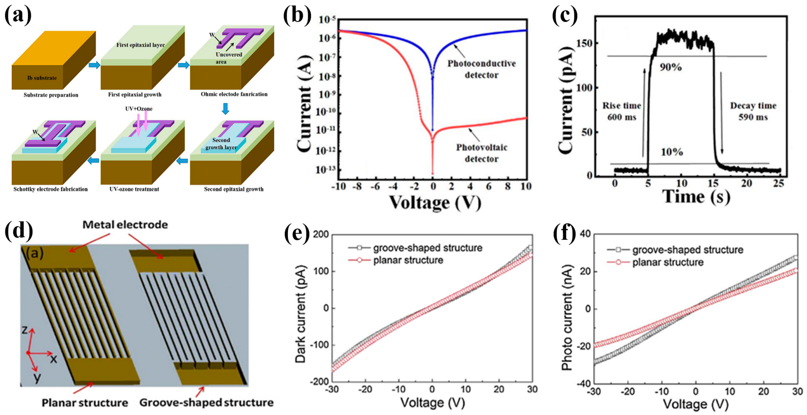
- Liu, K.; Dai, B.; Ralchenko, V.; Xia, Y.; Quan, B.; Zhao, J.; Shu, G.; Sun, M.; Gao, G.; Yang, L.; et al. Single crystal diamond UV detector with a groove-shaped electrode structure and enhanced sensitivity. Sens. Actuators A Phys. 2017, 259, 121–126. [Google Scholar] [CrossRef]
- Liu, Z.; Zhao, D.; Min, T.; Wang, H. 3D TiO2/Diamond Ultraviolet Detector Using Back-to-Back Pd Schottky Electrode. Phys. Status Solidi A-Appl. Mater. Sci. 2020, 217, 2000218. [Google Scholar] [CrossRef]
- Forneris, J.; Giudice, A.L.; Olivero, P.; Picollo, F.; Re, A.; Marinelli, M.; Pompili, F.; Verona, C.; Rinati, G.V.; Benetti, M.; et al. A 3-dimensional interdigitated electrode geometry for the enhancement of charge collection efficiency in diamond detectors. EPL Europhys. Lett. 2014, 108, 18001. [Google Scholar] [CrossRef] [Green Version]
- Lin, C.-N.; Lu, Y.-J.; Yang, X.; Tian, Y.-Z.; Gao, C.-J.; Sun, J.-L.; Dong, L.; Zhong, F.; Hu, W.-D.; Shan, C.-X. Diamond-Based All-Carbon Photodetectors for Solar-Blind Imaging. Adv. Opt. Mater. 2018, 6, 1800068. [Google Scholar] [CrossRef]
- Liao, M.; Sang, L.; Teraji, T.; Imura, M.; Alvarez, J.; Koide, Y. Comprehensive Investigation of Single Crystal Diamond Deep-Ultraviolet Detectors. Jpn. J. Appl. Phys. 2012, 51, 090115. [Google Scholar] [CrossRef] [Green Version]
- Salvatori, S.; Pace, E.; Rossi, M.; Galluzzi, F. Photoelectrical characteristics of diamond UV detectors: Dependence on device design and film quality. Diam. Relat. Mater. 1997, 6, 361–366. [Google Scholar] [CrossRef]
- Liao, M.; Koide, Y.; Alvarez, J. Single Schottky-barrier photodiode with interdigitated-finger geometry: Application to diamond. Appl. Phys. Lett. 2007, 90, 123507. [Google Scholar] [CrossRef]
- Čermák, J.; Koide, Y.; Takeuchi, D.; Rezek, B. Spectrally dependent photovoltages in Schottky photodiode based on (100) B-doped diamond. J. Appl. Phys. 2014, 115, 053105. [Google Scholar] [CrossRef]
- Liao, M.; Wang, X.; Teraji, T.; Koizumi, S.; Koide, Y. Light intensity dependence of photocurrent gain in single-crystal diamond detectors. Phys. Rev. B 2010, 81, 033304. [Google Scholar] [CrossRef]
- Mohapatra, S.; Sahu, P.; Rath, S.; Sahoo, P.K.; Varma, S.; Murty, N.N. Impact of nitrogen induced defect dynamics on UV response of diamond photodetectors. Superlattices Microstruct. 2020, 142, 106504. [Google Scholar] [CrossRef]
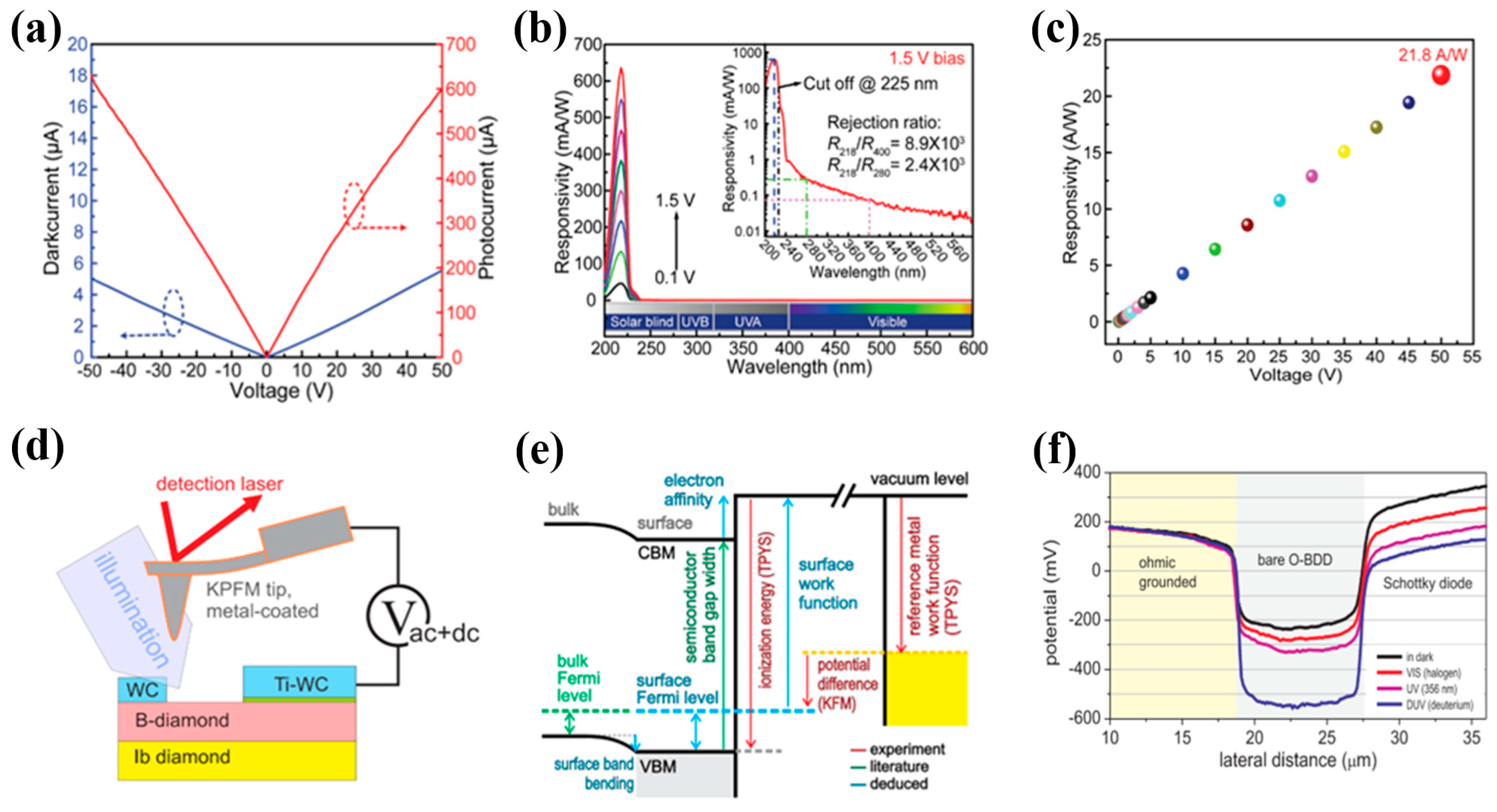
- Liu, B.; Liu, K.; Zhang, S.; Ralchenko, V.G.; Zhang, X.; Xue, J.; Wen, D.; Qiao, P.; Zhao, J.; Dai, B.; et al. Self-Powered Solar-Blind UV Detectors Based on O-Terminated Vertical Diamond Schottky Diode with Low Dark Current, High Detectivity, and High Signal-to-Noise Ratio. ACS Appl. Electron. Mater. 2022, 4, 5996–6003. [Google Scholar] [CrossRef]
- Liu, Z.; Lin, F.; Zhao, D.; Min, T.; Wang, H. Fabrication and Characterization of (100)-Oriented Single-Crystal Diamond p–i–n Junction Ultraviolet Detector. Phys. Status Solidi Appl. Mater. Sci. 2020, 217, 2000207. [Google Scholar] [CrossRef]
- Ge, L.; Peng, Y.; Wang, X.; Wang, D.; Xu, M.; Xu, X. Diamond Metal-Semiconductor Field-Effect-Transistor-based Solar Blind Detector. In Proceedings of the 2021 18th China International Forum on Solid State Lighting & 2021 7th International Forum on Wide Bandgap Semiconductors, Shenzhen, China, 6–8 December 2021. [Google Scholar]
- Wei, M.; Yao, K.; Liu, Y.; Yang, C.; Zang, X.; Lin, L. A Solar-Blind UV Detector Based on Graphene-Microcrystalline Diamond Heterojunctions. Small 2017, 13, 1701328. [Google Scholar] [CrossRef]
- Zkria, A.; Gima, H.; Yoshitake, T. Application of nitrogen-doped ultrananocrystalline diamond/hydrogenated amorphous carbon composite films for ultraviolet detection. Appl. Phys. A 2017, 123, 115102. [Google Scholar] [CrossRef]
- Chen, Y.C.; Lu, Y.J.; Lin, C.N.; Tian, Y.Z.; Gao, C.J.; Dong, L.; Shan, C.X. Self-powered diamond/β-Ga2O3 photodetectors for solar-blind imaging. J. Mater. Chem. C 2018, 6, 5727–5732. [Google Scholar] [CrossRef]
- Liu, Z.C.; Li, F.; Wang, W.; Zhang, J.W.; Lin, F.; Wang, H.X. Effect of depth of Buried-In Tungsten Electrodes on Single Crystal Diamond Photodetector. MRS Adv. 2016, 1, 1099–1104. [Google Scholar] [CrossRef]


| Material | Eg (eV) | Thermal Conductivity (W cm−1 K−1) | Melting Point (K) | Electron Saturation Velocity (107 cm S−1) | Mobility (cm2 V−1 S−1) Electrons/Holes | Dielectric Constant | Break Down Field (105 V cm−1) |
|---|---|---|---|---|---|---|---|
| Si | 1.12 | 1.5 | 1683 | 1 | 1400/600 | 11.8 | 3 |
| AlN | 6.2 | 3.19 | >2400 | 1.4 | 135/14 | 8.1 | 20 |
| AlGaN | 3.4–6.2 | ||||||
| BN | 5.9 | 2.35 in plane 2.3 × 10⁻² out of plane | 2970 | -/35 in plane | 6.85 in plane 5.06 out of plane | 80 | |
| Ga2O3 | 4.9 | 0.27 | 2 | 300/- | 10 | 80 | |
| Diamond | 5.5 | 20 | 3773 | 2.7 | 2200/1600 | 5.5 | 100 |
| Quantity | Symbol | Unit | Definition |
|---|---|---|---|
| Responsivity | R | A W−1, V W−1 | The ratio of photogenerated current or voltage to the incident light power |
| External quantum efficiency/internal quantum efficiency | EQE/IQE | / | In a photodiode, the ratio of the recombination number of electron–hole pairs that generate photocurrent to the number of incident/absorbed photons |
| Photoconductive gain | G | / | In a photoconductor, the ratio of the number of electrons collected by the electrode to the number of incident photons |
| Dark current | Idark | A | Current flowing in the photodetector without light |
| Response speed | τr/τd | s | Rise time (τr) and decay time (τd) are defined as the time needed for the photoresponse to increase from 10% to 90% or drop from 90% to 10% of its peak value |
| Noise current | Inoise | A Hz−1/2 | The random root means square fluctuation in current when bandwidth is limited to 1 Hz |
| Noise-equivalent power | NEP | W Hz−1/2 | The minimum impinging optical power required to achieve a signal-to-noise ratio of unity in a 1 Hz bandwidth |
| Specific detectivity | D* | cm Hz−1/2 W−1/Jones | A parameter for comparing the sensitivity between photodetectors with different device area A and bandwidth B. D* = (AB)−1/2/NEP |
| Response rejection ratio | Ra/Rb | / | The ratio between responsivity at light wavelength-a and that at light wavelength-b |
| Device Structure | Fabrication Method | Light of Detection/nm | Dark Current | On/Off Ratio | Rejection Ratio | Specific Detectivity/Jones | EQE | Responsivity | Rise Time/ Decay Time | Ref. |
|---|---|---|---|---|---|---|---|---|---|---|
| BNNS Photoconductor | PLD | 254 | <0.4 nA @50 V | UV/vis 108 | 0.6 ms/ 1.8 ms | [20] | ||||
| BN-WN nanocomposites Photoconductor | PLD | 250 | 1.17 A/W @2 V | <2 ms | [21] | |||||
| BNNS MSM | PLD | 254 | −200 nA | 1.5 mA/W @−5 V | [23] | |||||
| BNNS MSM | PLD | 250 | 9 μA/W@0 V | [24] | ||||||
| BNNS Schottky | PLD | 250 | 0.4 nA | 250/350 160~200 | 296 mA/W @0 V | 1.6 s/ 17 s | [18] | |||
| BN Nanopaper | - | 185 | 8.05 × 10¹⁰ | 0.267 s/ 0.393 s | [40] | |||||
| BN film Photoconductor | IBSD | 212 | 1.8 × 10¹⁰ | 1.33 mA/W @25 V | 1.04 ms/ 1.08 ms | [25] | ||||
| BN film MSM | IBSD | 212 | 204 >103 | 204/250 >103 | 6.92 × 10⁹ | 0.5 A/W @35 V | [27] | |||
| BN film MSM | IBSD | 212 | 5.3 × 10⁴ | 3.09 × 10¹¹ | 9.2 mA/W @20 V | <0.5 ms | [26] | |||
| BN film MSM | IBSD | 212 | 212/284 103 | 2.4 × 10⁸ | 0.1 mA/W @20 V | 0.32/0.63 s | [14] | |||
| BN film MSM | LPCVD | 224 | <10 pA @20 V | >312 | [30] | |||||
| BN film MSM | APCVD | 220 | 102 fA | 220/290 104 | 3.9 × 10¹⁰ | 3.4 mA/W @20 V | 120 ms/ 160 ms | [32] | ||
| BN film MSM | APCVD | 210 | 0.9 pA | 45 | 8.62 × 10⁹ | 5.45 mA/W @5 V | 376 ms/ 198 ms | [33] | ||
| BN film MSM | mechanically exfoliated | 215 | 3.68 × 10⁸ | 53.76μA/W @20 V | 0.38 s/ 0.77 s | [28] | ||||
| BN film MSM | mechanically exfoliated | 160 | 160/250 104 | 2133 | 2.75 A/W @20 V | 0.3 ms/ 14 ms | [29] | |||
| BN film Schottky | solid-state reaction | 210 | 102 | 6.1 × 10¹² | 2945 | 5.022 A/W @5 V | 0.2 s/ - | [38] |
| Device Structure | Fabrication Method | Light of Detection/nm | Dark Current | On/Off Ratio | Rejection Ratio | Specific Detectivity/Jones | EQE | Responsivity | Rise Time/ Decay Time | Ref. |
|---|---|---|---|---|---|---|---|---|---|---|
| AlN nanowire photoconductor | CVD | 325 | 20 | 2.7 × 10⁶ A/W @40 V | ~1 ms | [49] | ||||
| AlN nanowire photoconductor | LPCVD | 254 | 7.7 s/ 11.5 s | [51] | ||||||
| AlN micro/nanowire MSM | PVT | 190 | <100 fA@20 V | VUV/UV-C ~104 | 254 | 0.39 A/W @50 V | <0.1 s/ <0.2 s | [52] | ||
| AlN nanowire MSM | LPCVD | 254 | 2.43 mA/W @15 V | 0.27 s/ 0.41 s | [53] | |||||
| AlN nanowire Schottky | LPCVD | 254 | 2.32 × 10¹² | 584 | 1187.5 mA/W@30 V | [54] | ||||
| AlN film 3D-MSM | MOCVD | 200 | 2.6 pA | 1.51 mA/W @0 V | [69] | |||||
| AlN film 3D-MSM | MOCVD | 200 | 4.2 pA@8 V | 8 mA/W@2 V | 2.61 ns/ 3 ns | [70] | ||||
| AlN film FC-3DMSM | MOCVD | 200 | 5.96 pA@8 V | 9.6 mA/W @2 V | 2.90 ns/ 2.92 ns | [70] | ||||
| AlN film MSM | PVD | 200 | 14.6 pA@5 V | 7835@−2 V | 0.6 mA/W @5 V | 0.9 s/ 1.8 s | [71] | |||
| AlN/AlGaN Heterostructures MSM | MOCVD | 240 | 10 pA@20 V | [73] | ||||||
| AlN/AlGaN HeterostructuresTFT | LP-MOCVD | 240 | 1.7 pA@20 V | >108 | 240/280 >102 | 1.5 × 10¹⁸ @20 V | 1.6 × 10⁵ A/W @20 V | 537.5 ps 3.1 us | [74] | |
| Ga2O3/AlN heterojunction p-n | sputter | 253 | 0.145 pA | 2.14 × 10⁴ | 5.98 × 10¹⁰ | 95.95 μA/W @0 V | 90 ms/ 116 ms | [75] | ||
| Gr/AlN/GaN Heterostructures p-i-n | MOCVD | 194 | 194/212 >103 | 16 | 25 mA/W @0 V | [76] |
| Device Structure | Fabrication Method | Light of Detection/ nm | Dark Current | On/Off Ratio | Rejection Ratio | Specific Detectivity/Jones | EQE | Responsivity | Rise Time/ Decay Time | Ref. |
|---|---|---|---|---|---|---|---|---|---|---|
| AlGaN nanowires PEC | MBE | 254 | 48.8 mA/W @0 V | 83/19 ms | [81] | |||||
| AlGaN Nanorods Photoconductor | MOCVD | 250–276 | 115 mA/W @3 V | [82] | ||||||
| AlGaN Film MSM | MOCVD | 275 | J < 2 × 10⁻⁹ A/cm2@−10 V | UV/vis >106 | 80 | 176 mA/W @0 V | [101] | |||
| AlGaN Film MSM | MOCVD | 1.2 × 10⁴ | UV/vis 2 × 10³ | 5 × 10⁴ | 2575 A/W @20 V | [87] | ||||
| AlGaN Film MSM | MOCVD | 266 | 1.7 × 10 mA/W @−1 V | 1.37 s/ 1.87 s | [89] | |||||
| AlGaN Film p-i-n | MOCVD | 289 | J = 1 × 10⁻⁹ A/cm2@10 V | >106 | DUV/vis >106 | 6.1 × 10¹⁴ | 92 | 211 mA/W @0 V | <13 ms/ <13 ms | [90] |
| AlGaN Film p-i-n | MOCVD | 289 | 4.2 pA | DUV/vis >106 | 4 × 10¹⁴ | 74.7 @0 V | <13 ms/ <13 ms | [91] | ||
| AlGaN Film p-i-n | MOCVD | 1.2 × 10⁴ | 2.3 × 10³ | 5 × 10⁴ | 2575 A/W @20 V | [92] | ||||
| AlGaN/GaN heterostructure APD | MOCVD | 240 | 1.67 × 10⁴ A/W @0.5 V | - /7 s | [96] | |||||
| AlGaN/GaN heterostructure photoconductive | MOCVD | 254 | 1.5 × 10⁴ A/W@10 V | [97] | ||||||
| AlGaN/GaN Heterostructure TFT | MOCVD | 261 | 3.4 × 10⁵ A/W @1 V | 100 ms | [98] | |||||
| AlGaN/GaN heterostructure TFT | MOCVD | 240 | 4.6 × 10³ A/W @0.5 V | 8.4 s/ 170 s | [99] | |||||
| AlGaN/GaN heterostructure TFT | MOCVD | 240 | 55.4 nA | 1.67 × 10⁴ A/W @0.5 V | -/ 7 s | [100] |
| Device Structure | Fabrication Method | Light of Detection/nm | Dark Current | On/Off Ratio | Rejection Ratio | Specific Detectivity/Jones | EQE | Responsivity | Rise Time/ Decay Time | Ref. |
|---|---|---|---|---|---|---|---|---|---|---|
| β-Ga2O3 nanowires Photoconductor | CVD | 255 | 2.44 × 10⁻¹⁰ | ~102 | 0.39 | 0.8 mA/W @10 V | [106] | |||
| β-Ga2O3 nanowires Photoconductor | CVD | 255 | ~102 | 1.37 | 3.4 mA/W @5 V | [107] | ||||
| β-Ga2O3 nanowires Schottky | Thermal oxidation | 254 | 10−11@−30 V | ~102 | 0.6 mA/W @10 V | 1 μs/ 64 μs | [108] | |||
| β-Ga2O3 nanowires Photoconductor | CVD | 250 | 10−11 | 103 | 2 × 10⁵ | 377 A/W | 0.21 s/ 7.11 s | [109] | ||
| Ga2O3 nanobelts Photoconductor | CVD | 250 | 1.1 × 10⁴ | UV/vis 106 | 187 | 37.6 A/W | 11.8 s <0.3 s | [110] | ||
| Ga2O3 nanobelts Schottky | CVD | 254 | 10−10 | 104 | 9.4 × 10³ | 19.3 A/W @1 V | <0.02 s | [111] | ||
| β-Ga2O3 microbelts TFT | Mechanical exfoliation | 254 | 7.75 uA | 254/365 2.93 | 7.05 × 10¹¹ | 8.8 × 10⁵ | 1.8×10⁵ A/W @−30 V | 0.76 s/ 1.78 s @0 V | [114] | |
| β-Ga2O3 nanosheets TFT | CVD | 254 | 4 × 10¹² | 1600 | 3.3 A/W @10 V | 30 ms/ 60 ms | [113] | |||
| β-Ga2O3 flakes MSM | Mechanical exfoliation | 254 | 0.28 pA | 1.37 × 10³ | 254/365 1.92 × 10³ | 3.73 × 10¹⁰ | 1.68 A/W @30 V | 1.76 s/ 0.53 s | [115] | |
| Ga2O3 film MSM | MBE | 266 | 50 | UVC/vis >103 | 0.21 A/W @5 V | 0.48 s/ 0.58 s | [117] | |||
| Ga2O3 film MSM | PLD | 255 | 104 | UV/vis 104 | 0.7 A/W @5 V | 2.4 s/ 1.6 s | [118] | |||
| Ga2O3 film MSM | PE-ALD | 250 | UV/vis 5.97 × 10⁴ | 8.74 × 10¹² | 22.19 A/W @5 V | [121] | ||||
| Ga2O3 film MSM | Sputter | 230 | 1.78 × 10⁵ | 0.553 A/W @5 V | 2 s/0.1 s | [122] | ||||
| Al: Ga2O3 film MSM | Sputter | 230 | 1.2 × 10¹³ | 708 | 1.38 A/W @5 V | [125] | ||||
| Al: Ga2O3 film MSM | Sputter | 230 | UV/vis 1.55 × 10³ | 1.37 × 10¹¹ | 70 mA/W @5 V | [126] | ||||
| Zr: Ga2O3 film p-i-n | Sputter | 185 | 104 | 23.6 | 35 mA/W @0 V | 0.12 s/ 0.08 s | [128] | |||
| Sn: Ga2O3 film MSM | Sol–gel preparation | 254 | 0.76 nA | 6 × 10³ | 3.21 × 10¹² | 164 mA/W @30 V | 0.42 s/ 0.20 s | [129] | ||
| Cd: a-Ga2O3 film TFT | Spin-coating | 260 | UV/vis 1.88 × 10⁴ | 1.71 × 10¹² | 1036 | 2.17 A/W @0.2 V | [131] | |||
| a-Ga2O3 film TFT | Sputter | 250 | UV/vis 103 | 1015 | 104 A/W@6 V | [133] | ||||
| β-Ga2O3 film TFT | Mechanical exfoliation | 250 | 2.98 × 10¹⁵ | 5.02 × 10⁹ | 1.01 × 10⁷ A/W @0.5 V | 0.2 s/ | [134] | |||
| β-Ga2O3 film TFT | - | 254 | 5.45 × 10¹³ | 1.15 × 10³ | 2.34 A/W @ 9 V | 29.38 s/ - | [135] | |||
| β-Ga2O3/SnO2 Heterojunction MSM | LPCVD | 254 | 21 nA | 9 × 10⁴ | 1.7 × 10¹⁵ | 7.4 × 10⁵ | 1532 A/W @50 V | 0.5 s/ 0.2 s | [136] | |
| β-Ga2O3/SnO2 Heterojunction MSM | LPCVD | 302 | 2.97 × 10¹⁴ | 1 × 10⁵ | 262 A/W @50 V | 26 s/ 3 s | [136] | |||
| Gr/β-Ga2O3 heterojunction | CVD | 254 | 5.92 × 10¹³ | 1.96 × 10⁴ | 39.3 A/W @20 V | 94.83 s/ 219.19 s | [138] | |||
| N: Gr/β-Ga2O3 heterojunction | CVD | 235 | 10 | 235/280 1.5 × 10² | 4 × 10¹⁰ | 8.8 | 12 mA/W @0 V | 1.67 s 0.3 s | [139] | |
| N: Gr/β-Ga2O3 heterojunction | CVD | 235 | 104 | DUV/UV 6.4 × 10² | 1.3 × 10¹² | 190 | 360 mA/W @0 V | 0.89 s 0.14 s | [139] | |
| β-Ga2O3/CuO heterojunction p-n | Electro spraying | 254 | 6.94 × 10⁻¹⁴ | 2.99 × 10⁶ | 4.44 × 10¹⁴ | 3.1 × 10⁶ | 6.33 × 10³ A/W @5 V | [140] | ||
| Ga2O3/V2O5 heterostructure p-n | MOCVD | 254 | 2 fA | 2.6 × 10⁷ | 240/400 6.02 × 10⁴ | 7.8 × 10¹³ | 9.7 | 19.8 mA/W @0 V | 67 ms/ 26 ms | [141] |
| β-Ga2O3/NiO heterojunction p-n | PLD | 254 | 1.09 nA | 9.15 × 10³ | 4.2 × 10⁹ | 4.27 mA/W @−15 V | 4.6 ms/ 7.6 ms | [142] | ||
| a-Ga2O3/CFP core–shell composites PEC | Sputter | 254 | 12.9 mA/W @0 V | 0.15 s/ 0.13 s | [143] | |||||
| β-Ga2O3/PANI heterojunction | CVD | 246 | 0.08 pA | UV/vis 102 | 21 mA/W @0 V | [144] |
| Device Structure | Fabrication Method | Light of Detection/nm | Dark Current | On/Off Ratio | Rejection Ratio | Specific Detectivity/Jones | EQE | Responsivity | Rise Time/ Decay Time | Ref. |
|---|---|---|---|---|---|---|---|---|---|---|
| B: diamond film Photoconductor | CVD | 220 | <1 pA | >107 | 210/630 >106 | [149] | ||||
| diamond film Photoconductor | PECVD | 220 | 1 pA | DUV/vis 108 | 6 A/W@3 V | <10 ns | [150] | |||
| diamond film MSM | CVD | 210 | 0.368 pA | UV/vis 50 | 7.86 mA/W @8 V | [176] | ||||
| diamond film MSM | MPCVD | 213 | UV/vis 9.6 × 10³ | 1.26 × 10¹³ | 328 | 56.3 A/W @50 V | 1.03 ns/1.05 ns | [154] | ||
| diamond film MSM | CVD | 225 | 225/400 6.8 × 10³ | 1.91 × 10¹² | 1029 @470 V | 0.19 mA/W @9 V | 2 ns/ 20 ns | [155] | ||
| diamond film 3D-MSM | MPCVD | 210 | 14.2 pA @5 V | 215/400 276 | 600 ms/ 590 ms | [159] | ||||
| diamond film 3D-MSM | HPHT | 215 | 215/600 2 × 10³ | 5.32 mA/W @2 V | [161] | |||||
| diamond film Schottky | MPCVD | 218 | UV/vis 218/400 8.9 × 10³ | 1.39 × 10¹² | 21.8 A/W @50 V | [163] | ||||
| diamond film Schottky | MPCVD | 220 | DUV/vis 106@30 V 108@−23 V | 20@30 V 10,000@−23 V | 37 mA/W @30 V 18 A/W @−23 V | <0.3 s @30 V ~10 s @−23 V | [164] | |||
| diamond film Schottky | CVD | UV | UV/vis 104~105 | 10 A/W @100 V | 1~10 ms | [165] | ||||
| diamond film Schottky | CVD | 220 | 7 fA | 2 × 10⁵ | 3.8 × 10¹² | 16.2 mA/W@0 V | [170] | |||
| B: diamond film p-i-n | MPCVD | 210 | UV/vis 103 | 1.69 A/W @5 V | [171] | |||||
| UNCD/a-C:H heterojunctions p-n | Plasma deposition | 254 | 5.11 × 10¹⁰ | 65 | 134 mA/W @−5 V | [174] | ||||
| diamond/β-Ga2O3 heterojunctions p-n | MPCVD | 244 | 37@0 V | UV/vis 1.4 × 10² | 6.9 × 10⁹ | 0.2 mA/W @0 V | [175] |
Disclaimer/Publisher’s Note: The statements, opinions and data contained in all publications are solely those of the individual author(s) and contributor(s) and not of MDPI and/or the editor(s). MDPI and/or the editor(s) disclaim responsibility for any injury to people or property resulting from any ideas, methods, instructions or products referred to in the content. |
© 2023 by the authors. Licensee MDPI, Basel, Switzerland. This article is an open access article distributed under the terms and conditions of the Creative Commons Attribution (CC BY) license (https://creativecommons.org/licenses/by/4.0/).
Share and Cite
Fang, W.; Li, Q.; Li, J.; Li, Y.; Zhang, Q.; Chen, R.; Wang, M.; Yun, F.; Wang, T. Deep Ultraviolet Photodetector: Materials and Devices. Crystals 2023, 13, 915. https://doi.org/10.3390/cryst13060915
Fang W, Li Q, Li J, Li Y, Zhang Q, Chen R, Wang M, Yun F, Wang T. Deep Ultraviolet Photodetector: Materials and Devices. Crystals. 2023; 13(6):915. https://doi.org/10.3390/cryst13060915
Chicago/Turabian StyleFang, Wannian, Qiang Li, Jiaxing Li, Yuxuan Li, Qifan Zhang, Ransheng Chen, Mingdi Wang, Feng Yun, and Tao Wang. 2023. "Deep Ultraviolet Photodetector: Materials and Devices" Crystals 13, no. 6: 915. https://doi.org/10.3390/cryst13060915
APA StyleFang, W., Li, Q., Li, J., Li, Y., Zhang, Q., Chen, R., Wang, M., Yun, F., & Wang, T. (2023). Deep Ultraviolet Photodetector: Materials and Devices. Crystals, 13(6), 915. https://doi.org/10.3390/cryst13060915