Abstract
Two-dimensional (2D) van der Waals (vdW) AIIIBVI semiconductor materials, such as InSe and GaSe, are of considerable interest due to their potential use in various microelectronics applications. The range of properties of materials of this class can be extended further through the use of quasi-binary alloys of the InSe(Te)-GaSe(Te) type. In this work, we study the effect of compositional and structural disorder in 2D In(Ga)Se(Te) on the band structure and electronic properties using first principles modeling. The results for In(Ga)Se demonstrate a noticeable decrease in the band gap for structures with a random distribution of indium and gallium cations, while for In(Ga)Te with a random cation distribution, metallization occurs. Changes in the compositional arrangement of chalcogens (there can be either the same or different atoms on each side of the vdW gap) lead to pronounced changes in the band gap, but no significant changes in topology are observed. In addition, a significant effect of the distance between the layers on the band gap under compression along the c axis was found for both alloys under study. An important point of our study is that van der Waals gap engineering is a very powerful tool to control the properties of 2D materials and its alloys.
1. Introduction
The discovery of graphene in 2004 marked a turning point in the field of 2D materials. Since then, researchers have been pushing the boundaries of materials science, discovering many 2D materials with even more possibilities. Of particular interest are materials with semiconductor properties. The first such class of 2D semiconductors was transition metal dichalcogenides with the generic formula MX2 (M = Mo, W; X = S, Se, Te), of which MoS2 is the most studied representative. A characteristic feature of such materials is their layered structure, where strongly (covalently) bonded layers are held together by weak van der Waals (vdW) forces. The covalently bonded layers are often referred to as monolayers, even though in reality they may have a different number of atomic planes. Thus, in the already mentioned transition metal dichalcogenides, a monolayer is an X-M-X sandwich, where a metal plane is located between two chalcogen planes. In the group of topological insulators, such as Sb2Te3, a monolayer is a quintuple layer with the Te-Sb-Te-Sb-Te stacking sequence. The class of 2D semiconductors is constantly expanding.
Such materials are often referred to as two-dimensional (2D) solids or vdW solids, even when they exist in bulk form. The constantly growing interest in these materials is associated primarily with an important unique property inherent in some two-dimensional materials—the ability to form extremely thin layers, which exists due to the presence of a weak dispersion interaction between atomic layers. Of particular interest to researchers are single-layer and few-layer slabs made of such materials.
Two-dimensional materials offer an excellent platform for understanding fundamental physical phenomena on the nanoscale due to their limited dimensionality. Their behavior differs from that of bulk materials, allowing scientists to explore and manipulate quantum effects. With a wide range of electrical conductivity, varying from insulators to superconductors, 2D materials hold the promise of creating advanced electronic devices that can outperform traditional technologies. Recently, there has been a new surge of interest among researchers in two-dimensional (2D) semiconductors, since such materials have significant potential for creating devices with ultimately low power consumption [1]. This characteristic also opens the way for applications in transparent and flexible electronics [2].
In addition, this weak interaction, called van der Waals (vdW), between layers in 2D semiconductors allows the creation of heterostructures with atomically sharp interfaces, regardless of their lattice constants. These and other promising properties open up a wide range of opportunities for the production of new materials with improved characteristics [3,4]. In addition to the above, the behavior of 2D semiconductors is strongly influenced by quantum size effects and interlayer interaction. These factors lead to a noticeable dependence of properties on the number of layers, which, in turn, leads to exciting phenomena such as valley polarization and topological effects [5,6]. Currently, intensive research and development is being carried out aimed at expanding the range of possibilities and developing methods for studying new functions in two-dimensional chalcogenides.
One of the effective approaches to control the functionality of van der Waals materials is the fabrication of quasi-binary alloys using isoelectronic materials. These alloys often exhibit properties that vary linearly between two end points in accordance with Vegard’s law [7], but it should be noted that a more complex behavior is also observed in such alloys [8,9,10].
Among the many 2D materials, InSe stands out as an attractive candidate for various applications, mainly due to its exceptional characteristics, including record high charge carrier mobility and high property anisotropy [11,12]. In addition, the band gap of InSe can be changed in a very wide range (from 1.4 to 2.6 eV) by simply manipulating the number of layers [13,14,15]. The properties of InSe can also be further controlled by inclusion of alloying elements such as GaSe and GaTe. Also, the possibility of varying the properties of the material exists under the condition of the formation of GaSe/InSe superlattices or engineering materials with an ordered or random distribution of cations and anions in individual layers. If we pay attention to layered hexagonal GaTe, then a similar rearrangement of the band gap in a wide range is observed in it, as in GaSe [16]. The hexagonal modification of GaTe, in contrast to its more common monoclinic counterpart, provides greater control over the band gap and is the object of study. The present work is devoted to the study of quasi-binary alloys composed of GaTe, InSe and GaSe using ab initio simulations as a research and analysis tool. Different distributions of cations and anions relative to the vdW gap were investigated. The influence of various structural transformations, such as deformation compression along the c-axis and lateral displacement of layers relative to each other, were also studied. Since real materials are often a mixture of different phases, one of these mixtures was also investigated.
2. Materials and Methods
III–VI semiconductors, such as GaTe, GaSe, and InSe, have various crystalline modifications associated with different stacking of individual monolayers relative to each other (Figure 1). These layers have the same internal structure and hexagonal symmetry, forming four atomic planes in which the elements of groups III and VI alternate in the sequence VI-III-III-VI. In our calculations, we chose the centrosymmetric space group P63/mmc from various possible space groups, which describes the symmetry of the β-polytype. This polytype will be selected as one of the most frequently encountered. In this case, the β-polytype consists of four sublayers. The first and fourth sublayers each contain three Se anions, and the second and third sublayers each contain three Ga cations. The vdW forces between monatomic layers of anions depend to some extent on the repulsion of cations, which in turn affects the Ga–Ga intralayer bond and the Se–Se interlayer distance. Various polymorphs for hexagonal structures III–VI are shown in (Figure 1).
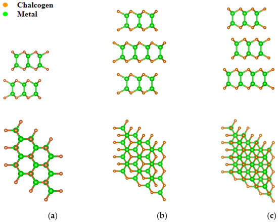
Figure 1.
The polymorphs of InSe: (a) β-phase; (b) γ-phase; (c) ε-phase. Upper panels—side view, lower panels—top view.
Unless otherwise stated, simulations were performed for the β-phase. All studied materials are united by the possibility of their use in various optical applications. GaSe has a band gap of approximately 1.65 eV and has been extensively studied for its potential applications in photoelectrochemistry and nanoscale photodetectors [17]. InSe has a band gap of ~1.26 eV, and it has been investigated for uses in field effect transistors (FETs) and photovoltaics due to its large absorption coefficient [18,19]. GaTe has a direct band gap of ~1.3 eV and has been studied for its potential applications in optoelectronics, photochemistry, and thermoelectricity due to its low thermal conductivity [20,21].
The density functional theory calculations were performed at 0 K using the CASTEP plane wave program [22]. Ultrasoft pseudopotentials were used. The Ga, Se, Te, and In pseudopotentials included the Ga 3d104s24p1, Se 4s24p4, Te 5s25p4, and In 4d105s25p1 electrons as valence electrons, respectively. The exchange term was estimated using the generalized gradient approximation (GGA) and the PBE functional [23] implemented in CASTEP. To ensure that the choice of functional did not affect the results, the structures were also optimized using the PBEsol solid-state potential (which did not affect the results). A study was made of the convergence depending on the cutoff energy of a plane wave and the Monkhorst-Pack grid, which were ultimately chosen to be 700 eV and 15 × 15 × 3, respectively, for the optimal combination of computational cheapness and accuracy. The following values were established by the criteria for simultaneous convergence: energy, 5 × 10⁻⁶ eV/atom; Max. strength—0.01 eV/A; Max. stress 0.02 GPa; Max. displacement 5 × 10⁻⁴ A. The optimization algorithm Two-Point Steepest Descent (TPSD) [24] was used. TPSD is a global optimization method and is suitable for quadratic potential problems. Thus, this method is effective when optimization of cells with custom constraints is required. The TPSD algorithm only requires the gradient and position of the system at the current and previous iteration, which means that it consumes relatively little memory. The TPSD method overcomes the limitations of descent algorithms while maintaining the advantages of point-to-point algorithms.
Another important factor is that, in connection with the long-range nature of dispersion interactions, it is necessary to more carefully study the convergence of energy in terms of the number of k-points. Therefore, the study of convergence depending on the corrections of the dispersion interaction was carried out. Subsequently, the MBD* method [25] was chosen as the correction for the van der Waals dispersion interaction, as it most accurately takes into account electronic correlations. The MBD* method is based on the random phase approximation for the correlation energy, where the response function is approximated by the sum of atomic contributions represented by quantum harmonic oscillators. This method sometimes has numerical problems if highly polarized atoms are located at short distances, which is a limitation of the underlying physical model. In Figure 2, we show the starting materials, their electronic structures, and the corresponding densities of states. From these structures, alloys of various configurations were subsequently prepared.
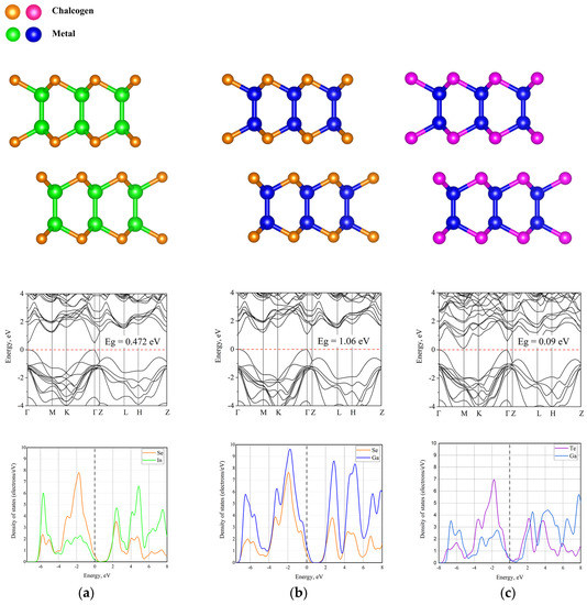
Figure 2.
Atomic (top), electronic (middle) structures and densities of states (bottom) of (a) InSe; (b) GaSe; (c) GaTe.
3. Results
3.1. Compositional Disorder
In the course of the study, we simulated the atomic and electronic structure of different 2D In(Ga)Se alloys. Ga and In can hypothetically be distributed in layered In(Ga)Se in several different ways. Namely, (i) InSe and GaSe layers may alternate forming an InSe/GaSe superlattice, or (ii) Ga and In can form monatomic planes such that the atomic plane sequence is the same in all layers and, finally, (iii) Ga and In may be distributed in the materials in a random way. Also, the terminating chalcogen atoms forming the vdW gaps can be distributed in different ways.
We start our investigation with differently distributed cations. Various possible atomic structures and the corresponding band structures are shown in Figure 3. One can see that the smallest band gap is obtained for the structure marked Ga-vdW-In. Here and below, we will indicate the alternation of sublayers in this way. This notation means that on one side of the vdW gap the nearest metal plane is formed by Ga atoms while at the opposite side the corresponding atomic plane is formed by In atoms. It should also be noted that, due to the boundary periodic conditions required by density functional simulations, the configurations Ga-vdW-Ga and In-vdW-In are identical. The largest gap, among structures with different distributions of metal atoms, is observed for the Ga-vdW-Ga (or In-vdW-In) structure (Figure 3b), where vdW gaps formed by metal atoms of the same nature alternate. In the case of a random distribution of cations, the band gap has an intermediate value, and it can be seen that the main extrema are shifted from the Γ point and blurred. As for the heterostructure, the band gap is slightly larger than for structures with different distributions of metal atoms. The topology of the zones does not have any significant differences compared to configurations with compositional permutations.
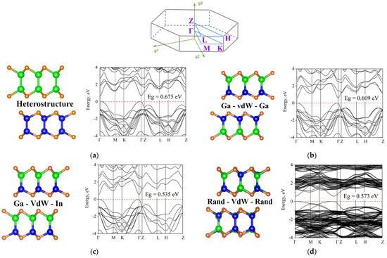
Figure 3.
At the top of the figure, the Brillouin zone is shown. Different compositions of the GaInSe and related band structures: (a) GaSe-InSe heterostructure; (b) Ga-vdW-Ga; (c) Ga-vdW-In; (d) randomly distributed cations. The color code is the same as in previous images.
An analysis of the partial density of states (PDOS) gives us an idea of the electron density distribution at and near the Fermi level (Figure 4). The PDOS analysis also shows the contributions of various atoms to the density of states. By analyzing the partial contributions from different atoms to the density of states, it becomes apparent that no significant changes occur; for all structures, the contribution of chalcogen atoms dominates both the top of the valence band and the bottom of the conduction band.
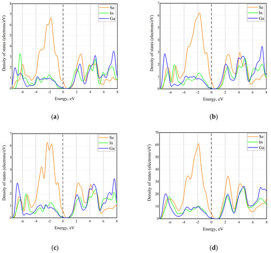
Figure 4.
Partial DOS from different atoms in different configurations of InGaSe alloy: (a) GaSe-InSe heterostructure; (b) Ga-vdW-Ga; (c) Ga-vdW-In; (d) randomly distributed cations.
Similar simulations were performed for the Ge(In)Te system. We note that the band gap in tellurides is smaller than in selenides, which is to be expected. The decrease in Eg in the series of compounds GaX (X = S, Se, Te) with an increase in the mass of the anion is associated with a decrease in the degree of ionicity of the Ga–X bond. It should also be noted that the experimental data available in literature for Eg of hexagonal GaTe demonstrate a significant scatter [16].
In the analysis of compositional rearrangements with tellurides, in contrast to the case in selenide structures, no significant change in the band gap is observed. The topology of the band structure for the Ga-vdW-Ga and Ga-vdW-In compositions does not change at all (Figure 5b,c). When switching to a random distribution, it is seen that the main extrema are blurred, and the maximum of the valence band is shifted to the L-point of the Brillouin zone. For the heterostructure, the band gap decreases in comparison with the initial GaTe structure (Figure 2c).
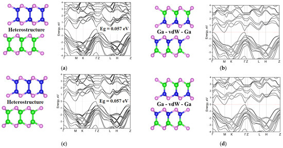
Figure 5.
Different compositions of the GaInTe and related band structures: (a) GaTe-InTe heterostructure; (b) Ga-vdW-Ga; (c) Ga-vdW-In; (d) randomly distributed cations. The color code is the same as in previous images.
Figure 6 shows PDOS for the studied GaInTe structures. While in general the results look similar to the case of selenides, viz., the major contribution to the PDOS comes from the chalcogen atoms, there is one interesting exception. Namely, in the GaTe-InTe heterostructure, the top of the valence band is formed by Te atoms, while the bottom of the conduction band is formed by the In atoms, i.e., Ga and In atoms, even if they are “identical” from the compositional perspective, contribute differently to the electronic structure. At this moment, it is not clear why this difference is only observed in tellurides and not in selenides.
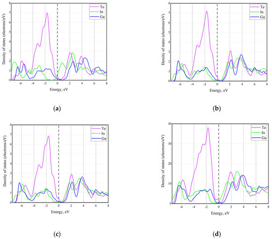
Figure 6.
Partial DOS from different atoms in different configurations of InGaTe alloy: (a) GaTe-InTe heterostructure; (b) Ga-vdW-Ga; (c) Ga-vdW-In; (d) randomly distributed cations.
Structures with different distributions of chalcogens in the layers and across the vdW gaps were also studied (Figure 7 and Figure 8). In this case, the differences between the various atom allocations are significant. When the vdW gap is formed by different (Te-vdW-Se) and identical (Se-vdW-Se) chalcogens, they differ significantly in their band gap. This is especially pronounced for Ga-based structures. As for the various distributions of chalcogens in the indium-based structure, such a significant change in the band gap does not occur—the range of changes is much smaller, but the general trend is similar.
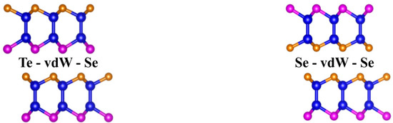
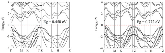
Figure 7.
Different compositions of the GaTe(Se) with different order of chalcogenide layers: (left) Te-vdW-Se, (right) Se-vdW-Se.
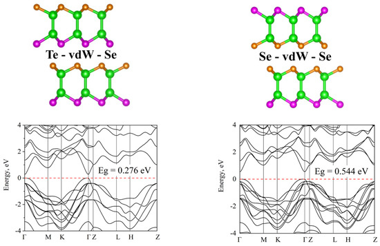
Figure 8.
Different compositions of the InSe (Te) with different order of chalcogenide layers: (left) Te-vdW-Se, (right) Se-vdW-Se.
It should be noted that in the case of structures in which the gap vdW is formed by chalcogen atoms of the same type, the topology also changes in addition to the band gap. One can see an increase in the extremum at the Z point of the Brillouin zone. This can be a little unexpected, as usually the topology changes due to a change in symmetry.
Thus, it becomes clear that it is the chalcogen atoms that have the most significant effect on the band gap. In the case of a change in the distribution of chalcogen atoms in the layers, the band gap changes in a wider range compared to the case when the metal atoms are rearranged. In this case, the topology of the band structure does not change significantly, which is natural, since changes in the topology should be associated to a greater extent with symmetry, as we saw, for example, for a random distribution of cations.
3.2. Structural Disorder
To further explore the effect of vdW interactions, we performed a series of simulations, influencing the band gap not by changing the composition of the atoms that form the vdW gap, but by changing the vdW gap width. Only the distance along the c-axis was changed (without changing other parameters and without structure) relaxation. The results are presented in Figure 9 and show that the band gap increases with an increase in the vdW gap.
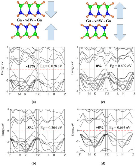
Figure 9.
The electronic structure of fully relaxed cell InGaSe (c = 17.55 Å) subjected to compression and stretching along the c-axis: (a) band gap decreases to 0.028 eV upon compression by 11%; (b) initial structure; (c) band gap decreases to 0.304 upon 5%; (d) increases to 0.693 eV upon stretching by 5%.
For selenium-based materials, compressing the materials along the c-axis eventually results in the formation of a gapless state. The band gap variation for both compression and stretching deformations can be approximated by linear dependencies, albeit the steepness of the curves is very different (Figure 10), which is most likely due to the anharmonicity of interatomic potentials. We also note that the topology of the zones changed insignificantly.
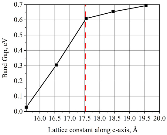
Figure 10.
Change in the InGaSe band gap width during a c-axis lattice constant variation. Starting with an ideal structure at the point (c = 17.55 Å).
In tellurides, an interesting effect of topology change is revealed during stretching, namely, the smearing of the extremum at the Z-point of the Brillouin zone. It is also worth noting a slight change in the position of the extremum at point M relative to the Fermi level during compression and tension by 5% (Figure 11).
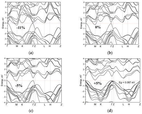
Figure 11.
The electronic structure of fully relaxed cell InGaTe (c = 17.19 Å) subjected to compression and stretching along the c-axis: (a–c) band gap is not noticeable for compressions 11%, 0%, and 5%, respectively; (d) increase to 0.087 eV upon stretching by 5%.
In contrast to the “vertical” displacement of monolayers with respect to each other, lateral displacement of layers without changing the interlayer distance did not demonstrate a similarly large change in the band gap, as is illustrated in Figure 12. It may be noted that such a displacement leads to a decrease in the band gap.
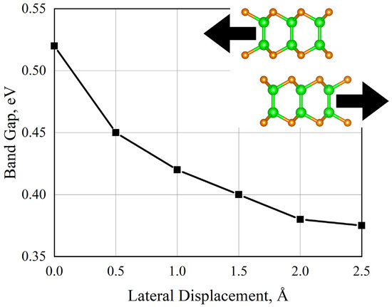
Figure 12.
Change in the electronic structure of the γ-phase of GaSe during a successive shift with a step of 0.5 Å. Zero on the horizontal axis corresponds to the ideal structure.
From these results, an interesting observation can be made. Although van der Waals interactions across the layers are significantly weaker than covalent bonds within layers, it is these weak vdW forces that play a decisive role in determining the band gap of 2D semiconductors. Indeed, during the lateral layer displacement, while the covalent structure of the monolayers was unchanged, the band gap decreased by 30% from the starting value. An important point from this finding is that vdW gap engineering is a very powerful tool to control the properties of 2D materials.
Real structures are often a mixture of phases. Thus, even in classic 3D semiconductors such as ZnS, ZnSb different stacking sequences may alternate between sphalerite and wurtzite phases. Phase alternation along the growth axis is even more natural for 2D semiconductors. In Figure 13 (left panel), we show a structure with alternating ϵ- and γ-phases. Figure 13 (right panel) shows that the band gap changes insignificantly, while the pattern appears to be highly dispersive, which we believe to be due to broken symmetry. The main extrema are shifted from the gamma point to Z-point. Otherwise, the topology of the zones and the value of the band gap are preserved.
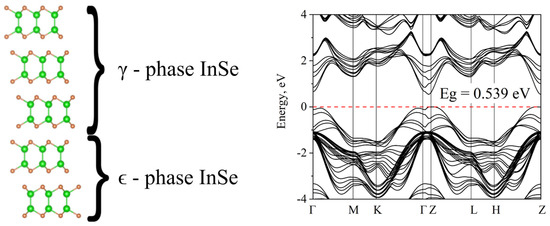
Figure 13.
Mixed γ and ϵ InSe phases. Atomic structure on the left and the corresponding band structure on the right.
4. Conclusions
In this work, we study the effect of compositional and structural disorder on the electronic properties of mixed structures of gallium and indium selenides and tellurides with a weak van der Waals interaction between the layers.
We found that random distribution of indium and gallium cations (for both tellurides and selenides) significantly affects the topology of the band structure, which we attribute as being due to symmetry breaking, while the band gap does not change significantly. On the other hand, the ordered distribution (one type of atoms in the atomic plane forming the vdW gap) does not significantly affect the topology, but only affects the band gap. Various permutations of the chalcogen atoms across the vdW gaps have also been studied and found to have a significant effect on the band gap value. In particular, it was found that the different distribution of Se and Te in Ga-based materials leads to the most significant changes in the band width; namely, in the case when the vdW gap is formed on both sides by atoms of the same type, the band width will be the largest.
The uniaxial tension and compression of materials has been investigated and a strong correlation between the van der Waals gap width and the electronic band gap has been found, which is confirmed by experimental data that can be found in the literature [26].
Lateral displacement of atoms, on the other hand, does not significantly affect the band gap; instead, a topology change was observed with a shift of the extremum towards the Z-point of the Brillouin zone. The mixing of the two phases occurs in a similar way. Due to the fact that the types of atoms in the sublayer that forms the VdW gap are the same, and the distance between the layers is preserved, the band gap changes insignificantly, while the topology changes significantly, and the extremum at the Z point shifts to the Fermi level. This is again explained by a change in symmetry without changing the distance between the layers and the type of atoms that form the gap (chalcogens).
Our study confirms the decisive influence of chalcogen atoms on the band structure and vdW gap. In this case, the largest expansion of the zone occurs when the gap is formed by atoms of the same type, and the smallest, when the gap is formed by atoms of different types.
We believe that our results are rather general and can be applied to other classes of 2D materials.
Author Contributions
R.S.S.—conceptualization, simulations, methodology, writing—original draft preparation; P.I.M.—simulations, visualization, software; A.V.K.—conceptualization, project administration, writing—review and editing. All authors have read and agreed to the published version of the manuscript.
Funding
This work was supported by the Russian Science Foundations under grant 22-19-00766.
Data Availability Statement
The data that support the findings of this study are available from the corresponding author upon reasonable request.
Conflicts of Interest
The authors declare no conflict of interest.
References
- Fiori, G.; Bonaccorso, F.; Iannaccone, G.; Palacios, T.; Neumaier, D.; Seabaugh, A.; Colombo, L. Electronics based on two-dimensional materials. Nat. Nanotechnol. 2014, 9, 768–779. [Google Scholar] [CrossRef]
- Zhang, X.; Li, J.; Zhou, X. Tunable bandgap and vacancy defects in GaSe/SnSe van der Waals heterostructure. J. Mater. Res. 2021, 36, 4927–4937. [Google Scholar] [CrossRef]
- Zhao, Q.; Frisenda, R.; Wang, T.; Castellanos-Gomez, A. InSe: A two-dimensional semiconductor with superior flexibility. Nanoscale 2019, 11, 9845–9850. [Google Scholar] [CrossRef]
- Bakaul, S.R.; Serrao, C.R.; Lee, M.; Yeung, C.W.; Sarker, A.; Hsu, S.L.; Salahuddin, S. Single crystal functional oxides on silicon. Nat. Commun. 2016, 7, 10547. [Google Scholar] [CrossRef]
- Kim, S.J.; Choi, K.; Lee, B.; Kim, Y.; Hong, B.H. Materials for flexible, stretchable electronics: Graphene and 2D materials. Annu. Rev. Mater. Res. 2015, 45, 63–84. [Google Scholar] [CrossRef]
- Zhang, Y.; Ding, W.; Chen, Z.; Guo, J.; Pan, H.; Li, X.; Xie, W. Layer-Dependent Magnetism in Two-Dimensional Transition-Metal Chalcogenides MnTn+ 1 (M= V, Cr, and Mn; T= S, Se, and Te; and n= 2, 3, and 4). J. Phys. Chem. C 2021, 125, 8398–8406. [Google Scholar] [CrossRef]
- Jeong, J.; Choi, Y.H.; Jeong, K.; Park, H.; Kim, D.; Cho, M.H. Evolution of the broadband optical transition in large-area MoSe2. Phys. Rev. B 2018, 97, 075433. [Google Scholar] [CrossRef]
- Srour, J.; Badawi, M.; El Haj Hassan, F.; Postnikov, A.V. Crystal structure and energy bands of (Ga/In) Se and Cu (In, Ga) Se2 semiconductors in comparison. Phys. Status Solidi 2016, 253, 1472–1475. [Google Scholar] [CrossRef]
- Gencarelli, F.; Vincent, B.; Demeulemeester, J.; Vantomme, A.; Moussa, A.; Franquet, A.; Heyns, M. Crystalline properties and strain relaxation mechanism of CVD grown GeSn. ECS J. Solid State Sci. Technol. 2013, 2, P134. [Google Scholar] [CrossRef]
- Bodlos, R.; Dengg, T.; Ruban, A.V.; Dehghani, M.; Romaner, L.; Spitaler, J. Ab-initio investigation of the atomic volume, thermal expansion, and formation energy of WTi solid solutions. Phys. Rev. Mater. 2021, 5, 043601. [Google Scholar]
- Li, X.; Li, L.; Wu, M. Various polymorphs of group III–VI (GaSe, InSe, GaTe) monolayers with quasi-degenerate energies: Facile phase transformations, high-strain plastic deformation, and ferroelastic switching. Mater. Today Phys. 2020, 15, 100229. [Google Scholar] [CrossRef]
- Sun, Y.; Li, Y.; Li, T.; Biswas, K.; Patanè, A.; Zhang, L. New polymorphs of 2D indium selenide with enhanced electronic properties. Adv. Funct. Mater. 2020, 30, 2001920. [Google Scholar] [CrossRef]
- Venanzi, T.; Arora, H.; Winnerl, S.; Pashkin, A.; Chava, P.; Patanè, A.; Schneider, H. Photoluminescence dynamics in few-layer InSe. Phys. Rev. Mater. 2020, 4, 044001. [Google Scholar] [CrossRef]
- Song, C.; Fan, F.; Xuan, N.; Huang, S.; Zhang, G.; Wang, C.; Yan, H. Largely tunable band structures of few-layer InSe by uniaxial strain. ACS Appl. Mater. Interfaces 2018, 10, 3994–4000. [Google Scholar] [CrossRef]
- Zhang, Z.; Yuan, Y.; Zhou, W.; Chen, C.; Yuan, S.; Zeng, H.; Zhang, W. Strain-induced bandgap enhancement of InSe ultrathin films with self-formed two-dimensional electron gas. ACS Nano 2021, 15, 10700–10709. [Google Scholar] [CrossRef]
- Kosobutsky, A.V.; Sarkisov, S.Y. Influence of size effects on the electronic structure of hexagonal gallium telluride. Phys. Solid State 2018, 60, 1686–1690. [Google Scholar] [CrossRef]
- Başol, B.M. Low cost techniques for the preparation of Cu (In, Ga)(Se, S)2 absorber layers. Thin Solid Film. 2000, 361, 514–519. [Google Scholar] [CrossRef]
- Gauthier, M.; Polian, A.; Besson, J.M.; Chevy, A. Optical properties of gallium selenide under high pressure. Phys. Rev. B 1989, 40, 3837. [Google Scholar] [CrossRef]
- Ghalouci, L.; Taibi, F.; Ghalouci, F.; Bensaid, M.O. Ab initio investigation into structural, mechanical and electronic properties of low pressure, high pressure and high pressure-high temperature phases of Indium Selenide. Comput. Mater. Sci. 2016, 124, 62–77. [Google Scholar] [CrossRef]
- Borisenko, E.; Borisenko, D.; Timonina, A.; Kolesnikov, N. Nonvariant polymorphic transition from hexagonal to monoclinic lattice in GaTe single crystal. J. Cryst. Growth 2020, 535, 125548. [Google Scholar] [CrossRef]
- Schwarz, U.; Syassen, K.; Kniep, R. Structural phase transition of GaTe at high pressure. J. Alloys Compd. 1995, 224, 212–216. [Google Scholar] [CrossRef]
- Clark, S.J.; Segall, M.D.; Pickard, C.J.; Hasnip, P.J.; Probert, M.I.; Refson, K.; Payne, M.C. First principles methods using CASTEP. Z. Für Krist.-Cryst. Mater. 2005, 220, 567–570. [Google Scholar] [CrossRef]
- Perdew, J.P.; Burke, K.; Ernzerhof, M. Generalized gradient approximation made simple. Phys. Rev. Lett. 1996, 77, 3865. [Google Scholar] [CrossRef]
- Barzilai, J.; Borwein, J.M. Two-point step size gradient methods. IMA J. Numer. Anal. 1988, 8, 141–148. [Google Scholar] [CrossRef]
- Tkatchenko, A.; DiStasio, R.A., Jr.; Car, R.; Scheffler, M. Accurate and efficient method for many-body van der Waals interactions. Phys. Rev. Lett. 2012, 108, 236402. [Google Scholar] [CrossRef]
- Segura, A. Layered indium selenide under high pressure: A review. Crystals 2018, 8, 206. [Google Scholar] [CrossRef]


Disclaimer/Publisher’s Note: The statements, opinions and data contained in all publications are solely those of the individual author(s) and contributor(s) and not of MDPI and/or the editor(s). MDPI and/or the editor(s) disclaim responsibility for any injury to people or property resulting from any ideas, methods, instructions or products referred to in the content. |
© 2023 by the authors. Licensee MDPI, Basel, Switzerland. This article is an open access article distributed under the terms and conditions of the Creative Commons Attribution (CC BY) license (https://creativecommons.org/licenses/by/4.0/).