Article

Observation of Metal–Insulator Transition (MIT) in Vanadium Oxides V2O3 and VO2 in XRD, DSC and DC Experiments

Faculty of Physics, Warsaw University of Technology, Koszykowa 75, PL-00-662 Warsaw, Poland
*
Author to whom correspondence should be addressed.
Crystals 2023, 13(9), 1299; https://doi.org/10.3390/cryst13091299
Submission received: 3 August 2023 / Revised: 8 August 2023 / Accepted: 9 August 2023 / Published: 23 August 2023
(This article belongs to the Special Issue Metal Oxides: Crystal Structure, Synthesis and Characterization)

Abstract

:
Due to metal–insulator transitions occurring in those compounds, materials and devices based on vanadium (III) and (IV) oxides draw increasing scientific attention. In this paper, we observed the transitions in both oxides using contemporary laboratory equipment. Changes in the crystallographic structure were precisely investigated as a function of the temperature with a step of 2 °C. Thermal effects during transitions were observed using differential scanning calorimetry. The DC conductivity of the materials was measured quasi-continuously as a function of the temperature. All the experiments were consistent and showed considerable hysteresis of the metal–insulator transition in both vanadium oxides.

1. Introduction

Vanadium (V) is an element situated in block d of the periodic table (thus belonging to the transition metal group) with electron configuration [Ar] 4s² 3d³. In theory, it can exist in numerous oxidation states, namely, −1, +1, +2, +3, +4 and +5. However, the following three are most likely to be stable in crystalline structures: +3, +4 and +5. Different oxidation states of vanadium ions in simple solutions or compounds (in particular in oxides) can be distinguished by various colours: +5 (orange to yellow), +4 (blue) and +3 (green) [1]. In these three oxidation states, 4s electrons are removed, followed by one, two or three 3d electrons, respectively. These electronic properties result in a plethora of crystalline and amorphous structures that different oxidation states of vanadium compose, exhibiting a wide variety of physical and chemical properties. As a natural consequence, vanadium materials meet the enormous interest of researchers worldwide.
Vanadium oxides—including the most popular, V 2 O 3 , V 3 O 5 , V O 2 , V 3 O 7 , V 2 O 5 , V 2 O 2 , V 6 O 1 3 and V 4 O 9 —have found numerous practical applications due to a wide variety of their physical and chemical properties [2]. V 2 O 3 finds its application as cathode material for lithium/sodium/potassium batteries [3,4], as catalyst for the chemical looping dry reforming of methane [5], in ammonium perchlorate decomposition [6], in hydrogen evolution reaction [7,8] and in oxygen evolution reaction [8], as well as in supercapacitors [9] or as an electromagnetic wave absorber [10]. V O 2 finds numerous optical, electrical, mechanical and electrochemical applications. It can be applied as an infrared regulator (e.g., in smart window devices [11]), or as plasmonic material [12,13], sensor [14,15], electrical switch [16] or memristor [17] in supercapacitors [18] or batteries [19]. The basic application of V 2 O 5 are batteries [20] and supercapacitors [21]. However, it is also of interest in the field of catalysis [22] and electrochromism [23,24]. Dozens of other applications of the aforementioned vanadium oxides and many others can be found, e.g., in Ref. [2] and references therein.
Due to metal–insulator transitions occurring in those compounds, materials and devices based on vanadium (III) and (IV) oxides draw increasing scientific attention. In this paper, we observed the transitions in both oxides using contemporary laboratory equipment. Changes in the crystallographic structure were precisely investigated as a function of the temperature with a step of 2 °C. Thermal effects during transitions were observed using differential scanning calorimetry. The DC conductivity of the materials was measured quasi-continuously as a function of the temperature. All the experiments were consistent and showed considerable hysteresis of the metal–insulator transition in both vanadium oxides.
Additionally, more complex compounds containing vanadium attract much attention. In particular, the easiness of vanadium to exist in several oxidation states is the reason why many investigated cathode materials for lithium or why sodium batteries contain vanadium. The list includes but is not limited to, e.g., the aforementioned V 2 O 5 [20,25], L i V O P O 4 [26], L i V P O 4 F [27], N a 3 V 2 ( P O 4 ) 3 [28], N a 3 V 2 ( P O 4 ) 2 F 3 [29] and many others.
In this paper, we only focus on V O 2 and V 2 O 3 . They are particularly interesting because they exhibit temperature-induced phase transitions that result in spectacular alterations in the electronic properties. Namely, the low-temperature phases exhibit insulating properties, whereas the high-temperature phases are characterised by good electronic conductivity (metallic-like).
V O 2 (vanadium dioxide) can exist in various polymorphic phases, including V O 2 (B), V O 2 (A), V O 2 (M), V O 2 (R), V O 2 (D) and V O 2 (P) [30]. At room temperature, it adopts a monoclinic phase with the following unit cell parameters: a = 5.75 Å, b = 4.52 Å, c = 5.38 Å, β = 122.6 ° [31]. This phase is often referred to as an insulating phase (semiconductor-like). The metal-to-insulator transition in V O 2 was first predicted by Mott in 1949 [32]. It was later demonstrated in 1959 by Morin [33] that upon heating at 335–350 K, the monocrystals of V O 2 undergo a phase transition to highly conducting (called metallic) tetragonal rutile phase with the following unit cell parameters: a = b = 4.55 Å, c = 2.86 Å. Morin also observed hysteresis in the transition: upon cooling, the MIT effect appeared within 340–325 K. Although much effort was put into understanding the metal-to-insulator transition phenomenon in vanadium dioxide, the question remains open. In the monoclinic phase with lower symmetry, two varying lengths of V–V bonds are formed: 3.12 and 2.65 Å. The d electrons of vanadium play a major role in its conduction. It has been suggested that such V–V dimer formation directly leads to the change from the high-temperature delocalised state to the localized (insulating) state [34], as explained by the Peierls model [2]. Alternatively, the Mott–Hubbard model states that the MIT occurs when the electron density ( n e ) and Bohr radius ( a H ) satisfy n e 1 / 3 a H 0.2 [35]. A summary of numerous experiments addressing an in-depth investigation of this issue is provided, e.g., in Ref. [36].
As the MIT occurs in V O 2 at a temperature slightly higher than room temperature, its observation is relatively easy. The temperature dependency of the electronic resistivity of vanadium dioxide can be found in many papers, e.g., [37,38,39,40,41,42]. It is striking that even though some electrical data were provided by Morin in 1959 [33], most of the good-quality electrical measurements were published no earlier than 15 years ago. The XRD patterns of the room-temperature monoclinic phase and high-temperature tetragonal structure are well known. Surprisingly, it is much harder to find temperature-dependent studies of the crystallographic structure of vanadium dioxide with small temperature steps. An example of such experiment was reported by Chang et al. [38], who observed the (200) XRD reflex around 340 K. Differential scanning calorimetry is another experimental technique used for the observation of phase transitions and other thermal events occurring in materials, e.g., glass transition, crystallisation, melting, etc. While the MIT can also be detected with this method, DSC experiments on V O 2 are rather rare. Such observations were carried out by, e.g., Wang [43], Li [44] (undoped and W-doped), Takai [45], Muramoto [46] ( V O 2 -dispersed glass). Additionally, in our group, traces of the MIT of V O 2 in M V 2 O 5 P 2 O 5 glasses and nanomaterials were observed using DSC and DC measurements [47]. Further extensive information about vanadium dioxide can be found, e.g., in Refs. [48,49,50].
On the contrary, V 2 O 3 exhibits a highly conductive paramagnetic corundum-type hexagonal structure (spacegroup: R 3 ¯ c ) with lattice parameters of a = b = 4.9492 ( 2 ) Å, c = 13.988 ( 1 ) Å at room temperature [51]. It was also Morin [33] who reported the occurrence of the MIT effect in V 2 O 3 at 153 K and 165 K upon cooling and heating, respectively. Upon cooling, the phase changes to an antiferromagnetic insulating monoclinic structure (spacegroup i 2 / a ) with the following unit cell parameters at 165 K: a = 7.2727 ( 4 ) Å, b = 5.0027 ( 3 ) Å, c = 5.5432 ( 3 ) Å, β = 96.762 ( 2 ) ° [52]. While calling V 2 O 3 in this phase “Mott insulator”, the bandgap is reported to be 0.6 eV, a typical value for many semiconductors [53].
Since the MIT in V 2 O 3 occurs at ca. 160 K, its observation requires, e.g., liquid nitrogen cryostats. Therefore, papers reporting the metal–insulator transition in V 2 O 3 are less common than those on V O 2 . A schematic plot of V 2 O 3 conductivity was given by Morin in 1959 [33], followed by McWhan in 1973 [54] and Rozier in 2002 [52]. More recently, Trastoy showed resistivity plots for V 2 O 3 thin films [55], and Navarro studied light-induced changes in the resistivity of V 2 O 3 thin films [56]. Rozier also showed good-quality XRD patterns acquired at several fixed temperatures below and above the metal–insulator transition [52]. Thermal analyses of V 2 O 3 are very rare. Sujith reported some noisy DSC curves of V 2 O 3 in his master thesis [57]. Results of another DSC experiment were published by Zhang for V 2 O 3 /C composites [58].
As mentioned above, the metal-to-insulator transitions in vanadium (III) and (IV) oxides were discovered decades ago and, ever since, have been observed by some researchers. However, many of these observations were taken years ago. Naturally, their accuracy was limited by the capabilities of experimental techniques available at that time. Some experiments were carried out recently, quite often as supplementary or reference measurements to more complex research. This is why we decided to carry out observations of the MIT effect in V O 2 and V 2 O 3 using differential scanning calorimetry (DSC), X-ray diffractometry and electrical DC measurements using contemporary high-precision acquisition equipment and collect all these observations in one paper. This approach allowed us to revise the previous observations, as well as provide some new interesting experiments, e.g., XRD measurements in the quasi-continuous temperature domain.

2. Materials and Methods

In this work, two commercially purchased vanadium oxides were investigated: V O 2 (Aldrich, St. Louis, MO, USA; 99.99%) and V 2 O 3 (Sigma-Aldrich, St. Louis, MO, USA; 99.9%). Both materials were investigated in a corresponding range of temperature, namely, V O 2 from room temperature to ca. +100 °C and V 2 O 3 from room temperature down to ca. 175 °C.
Thermal effects related to the metal–insulator transition were observed with differential scanning calorimetry (DSC). For V O 2 , a TA Q200 device was used. For V 2 O 3 , a TA Q2000 device cooled with liquid nitrogen was necessary to reach the desired temperature range. Samples were encapsulated in TZero hermetic pans/lids in a glove box filled with dry argon to prevent any oxidation processes. Measurements were carried out at low heating/cooling rates, namely, 1 °C/min for V O 2 and 2 °C/min for V 2 O 3 .
X-ray powder diffraction data were collected using Cu-K α radiation ( λ 1 = 1.54056 Å and λ 2 = 1.54439 Å), filtered by focusing an X-ray mirror using a PANalytical Empyrean Series 2 diffractometer, and fitted with a PIXcel3D detector. The measurement was conducted in transmission geometry, with the powder loaded into the glass borosilicate capillary. Low-temperature measurements were performed using an Oxford Cryostream 800S cooler system supplied with liquid nitrogen stream over the temperature range from room temperature to 170 °C. Observations of the phase transitions were carried out using two approaches. Firstly, the patterns were acquired over the 2 Θ range from 20° to 70° or 80° (for V O 2 and V 2 O 3 , respectively), in steps of 0.0263° with an effective count time of 450 s per step. The temperature step was set to 10 °C in the case of V O 2 and 25 °C in the case of V 2 O 3 . This stage was to observe differences between the patterns of high- and low-temperature phases and to determine the “fingerprints” of each pattern. Secondly, the measurements were carried out in 2 Θ fixed-position mode. In such a mode, the angular range of a detector was equal to 3.347°. The positions were set to 27.5° and 54.0°in the cases of V O 2 and V 2 O 3 , respectively. The counting time was set to 175–220 s, and the temperature step was as low as 2 °C between each acquisition instance. Therefore, quasi-continuous measurements as a function of the temperature were possible.
The electrical conductivity of the samples was studied as a function of the temperature in corresponding temperature ranges. Powders kept in a glove box were transferred in a hermetic bottle to a pelleting setup. Pellets of 8 mm in diameter and ca. 2 mm in thickness were quickly pressed under ambient conditions and immediately moved to a Pt sputter. Then, the Pt electrodes were sputtered on the samples in low-pressure Ar atmosphere. The side layers of Pt electrodes were removed just before the measurements. Such a procedure limited the risk of oxidation of vanadium ions. The measurements of V O 2 were carried out in a tube furnace (Czylok) in argon flow. A Eurotherm 2404 temperature controller provided temperature stabilisation as good as 0.1 °C. An additional thermocouple was used to measure the temperature in the very proximity of the sample. The measurements of V 2 O 3 were carried out in a nitrogen-flow cryostat. The sample was kept in a hermetic chamber under high vacuum during measurement. Lakeshore 331 was used for temperature stabilisation and, additionally, to read the temperature from a Pt resistor situated next to the sample. The presence of the second temperature sensor in both cases was necessary to avoid differences between the setpoint temperature and the exact temperature of the sample. A home-made stable programmable voltage power source was used along with a precise Keithley Picoammeter 6485. The values of the current flowing through the sample were acquired each time the temperature changed by 0.5 °C. Hence, the ohmic resistance was calculated as a function of the temperature: R ( T ) = U / I ( T ) .

3. Results

3.1. Differential Scanning Calorimetry (DSC)

In Figure 1a, the DSC trace of V O 2 upon heating to 150 °C and subsequent cooling is shown. The heating/cooling rate in this experiment was as low as 1 °C/min. Upon heating, a distinct endothermic peak is observed with onset at T 10 = 60.1 °C and extremum at T 1 = 65.1 °C. The area under the peak represents the total heat of the transition and was equal to Q 1 = 30.0 J/g. Upon cooling, a much wider exothermic maximum appears, with onset at T 20 = 64.9 °C and the first extremum at T 2 = 59.6 °C. The peak spreads to temperatures as low as ca. 30 °C. The heat of this transition was calculated to be Q 2 = 29.8 J/g. The origin of the peak splitting is unclear.
In Figure 1b, the DSC trace of V 2 O 3 upon cooling down to 170 °C and subsequent heating is shown. The heating/cooling rate in this experiment was set to 2 °C/min. Upon cooling, a distinct exothermic peak is observed with onset at T 10 = 116.2 °C and extremum at T 1 = 118.7 °C. The area under the peak was equal to Q 1 = 9.8 J/g. Upon heating, a slightly narrower endothermic maximum appears, with onset at T 20 = 110.6 °C and the maximum at T 2 = 108.4 °C. The heat of this transition was calculated to be Q 2 = 10.7 J/g.

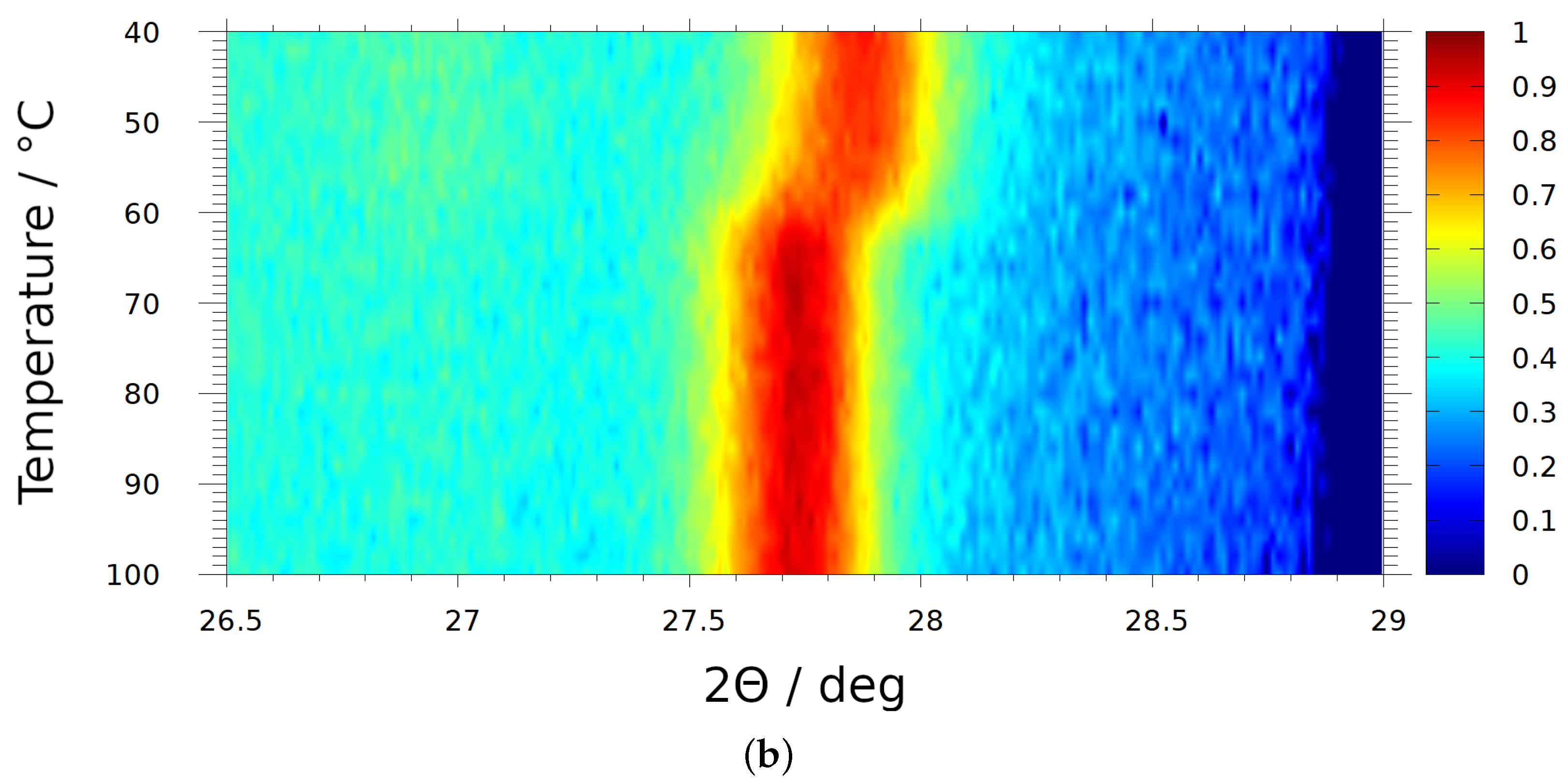
3.2. X-ray Diffractometry (XRD)

In Figure 2, the XRD patterns of V O 2 collected upon heating from 50 to 90 °C and subsequent cooling are shown. The temperature step between subsequent measurements was 10 °C. One can observe a change in the structure firstly occurring between 60 and 70 °C. This is demonstrated by the splitting of a peak centred at 65.2° and by a subtle shift in the peak initially centred at 28.1°. The physical reason standing behind these observation is the change in the unit cell of V O 2 . Upon heating, the monoclinic structure changes to a tetragonal one with a higher symmetry. A reversed behaviour is observed upon cooling, between 60 and 50 °C.
In order to determine the temperature of the structure change with better accuracy, the detector position remained fixed in the next experiment, and the signal was collected each time the temperature changed by 2 °C. Therefore, a quasi-continuous observation of the transition was possible, as visualised in Figure 3a,b. For this observation, both fingerprints mentioned in the previous paragraph could be utilised. Eventually, the position of the first peak was chosen due to its significant intensity. In Figure 3a, the position of the peak upon heating is shown. The shift begins at 60 °C and lasts until 66 °C. Later, its position remains almost fixed (only a little shift due to thermal expansion may be observed) until the maximum temperature of the ramp, namely, 100 °C. In Figure 3b, the position of the peak upon subsequent cooling is shown. Now, the position is held until ca. 64–66 °C, when smooth change is observed until a temperature as low as ca. 44 °C is reached.
From the XRD measurements of V O 2 , we can draw the following observations:
  • Evidence of phase transition hysteresis is given, as the transition proceeds at 60 66 °C upon heating and 66 44 °C upon cooling;
  • The transition is wider upon cooling (ca. 22 °C) than upon heating (ca. 6 °C).
A similar experiment was performed for V 2 O 3 . This time, XRD patterns of V 2 O 3 were collected with Δ T = 25 °C upon cooling from −70 to −170 °C and subsequent heating up to 70 °C (Figure 4). This time, a visible change in XRD patterns is firstly observed between 120 and 145 °C, namely, a split of single peaks originally centred at ca. 24.5, 33, 41.4, 50, 54.1 and 63.3°. The most pronounced fingerprint of the transition is a split of the most intense peak (centred at 54.1°) into three peaks of lower intensity. Upon heating, the patterns remain unchanged until −120 °C. A reversed transition is not observed until −95 °C. These observations are a manifestation of a phase transition from the low-temperature monoclinic structure to the high-temperature hexagonal corundum-like structure.
Once again, in order to determine the temperature of the structure change with better accuracy, the detector position remained fixed around 54 ° in the next experiment, and the signal was collected each time the temperature changed by 2 °C (Figure 5a,b). Upon cooling (Figure 5a), the single peak begins to disappear at 120 °C. The shape of three low-intensity peaks clarifies around 128 °C and remains stable until the end of the cooling ramp, namely, 170 °C. Upon heating (Figure 5b), the three peaks begin to diminish at 114 °C, and a high-intensity peak forms at ca. 108 °C.
In contrast to V O 2 , in V 2 O 3 , the temperature width of the phase transition was similar upon cooling and heating (ca. 6–8 °C). On the other hand, similar hysteresis was observed, as the transition was observed at 118 128 °C upon cooling and 114 108 °C upon heating.

3.3. DC Conductivity

The electrical conductivity of V O 2 upon heating to 135 °C and subsequent cooling is shown in Figure 6a. The material exhibited the value of conductivity of ca. 10 S/m at room temperature. Upon heating, above 60 °C, a stepwise deviation from Arrhenius dependency is observable. The increase in conductivity is smaller than one order of magnitude. Upon cooling, the conductivity is greater than 100 S/m. The setup was devoted to measurements of high-resistance samples. Thus, considerable noise is observable at low resistance/high conductance values. Below 60 °C, another stepwise drop in conductivity is observed. These reversible changes in conductivity are in agreement with our previous measurements of vanadate–phosphate glasses and nanomaterials, where the presence of V O 2 precipitates was suspected (Figure 5 in Ref. [47]).
The electrical conductivity of V 2 O 3 upon cooling from 0 °C down to 135 °C and subsequent heating is shown in Figure 6b. On a logarithmic scale, the values of conductivity in the “conducting” phase look almost constant. Below 115 °C, a distinct stepwise drop in conductivity is measured (ca. 2 orders of magnitude). Below the transition, the dependence of conductivity follows the Arrhenius formula. Upon heating, a stepwise increase in conductivity is observed at ca. 110 °C, and conductivity returns to the previous values. In the case of V 2 O 3 , hysteresis seems to be larger than in the case of V O 2 .

4. Discussion and Conclusions

In this work, metal-to-insulator transitions in vanadium oxide (IV) and (III) were investigated using contemporary equipment with differential scanning calorimetry, temperature-dependent X-ray diffractometry and electrical conductivity measurements. In such experiments, precise temperature control plays an essential role. In this work, DSC analysers were appropriately calibrated. In DC measurements, a secondary thermocouple situated in the very proximity of the sample was used to achieve high-accuracy temperature determination. Only in XRD measurements, the temperature was determined from the setpoint of the heater/cooler. Nevertheless, all the experimental results presented in this work were consistent. However, various methods showed different degrees of sensitivity to the detection of phase transitions.
The occurrence of the insulator-to-metal transition upon the heating of V O 2 was observed precisely above 60 °C in DSC, XRD and DC measurements. The transition was narrow and lasted until ca. 66 °C. On the contrary, upon cooling, the metal-to-insulator transition began at 64–66 °C but lasted longer, even until ca. 44 °C, as evidenced by XRD and DC measurements. In DSC measurements, the signal from this phenomenon was even wider, spreading down to 25 °C.
The width of the MIT transition in V 2 O 3 upon cooling and heating was similar, equal approximately to 10 and 6 °C, respectively. However, visible hysteresis was seen. Upon cooling, the transition process was observed between 118 and 128 °C (using XRD) or 115 and 125 °C (using DC). Upon heating, the transition was measurable above 114 / 110 °C (using XRD and DC, respectively) and lasted for about 6 °C.
This work shows that the temperatures of phase transitions in V O 2 and V 2 O 3 well-established in the literature, namely, 67 °C and 123 °C, need to be taken with precautions. Especially in dynamic non-equilibrium experiments (heating/cooling at a rate of several °C/min), the temperatures of the transitions may be shifted and last as much as 10 °C.

Author Contributions

Conceptualization, T.K.P.; Investigation, P.P. and T.K.P.; Methodology, J.J. and T.K.P.; Supervision, T.K.P.; Visualization, P.P. and T.K.P.; Writing—original draft, P.P., J.J. and T.K.P. All authors have read and agreed to the published version of the manuscript.

Funding

This research received no external funding.

Data Availability Statement

Data are available from the authors upon reasonable request.

Conflicts of Interest

The authors declare no conflict of interest.

Abbreviations

The following abbreviations are used in this manuscript:
XRDX-ray diffractometry
DSCDifferential scanning calorimetry
DCDirect current
RTRoom temperature

References

  1. Rehder, D. The Future of/for Vanadium. Dalton Trans. 2013, 42, 11749–11761. [Google Scholar] [CrossRef] [PubMed]
  2. Hu, P.; Hu, P.; Vu, T.D.; Li, M.; Wang, S.; Ke, Y.; Zeng, X.; Mai, L.; Long, Y. Vanadium Oxide: Phase Diagrams, Structures, Synthesis, and Applications. Chem. Rev. 2023, 123, 4353–4415. [Google Scholar] [CrossRef]
  3. Han, C.; Liu, F.; Liu, J.; Li, Q.; Meng, J.; Shao, B.; He, Q.; Wang, X.; Liu, Z.; Mai, L. Facile Template-Free Synthesis of Uniform Carbon-Confined V2O3 Hollow Spheres for Stable and Fast Lithium Storage. J. Mater. Chem. A 2018, 6, 6220–6224. [Google Scholar] [CrossRef]
  4. Jin, T.; Li, H.; Li, Y.; Jiao, L.; Chen, J. Intercalation Pseudocapacitance in Flexible and Self-Standing V2O3 Porous Nanofibers for High-Rate and Ultra-Stable K Ion Storage. Nano Energy 2018, 50, 462–467. [Google Scholar] [CrossRef]
  5. Ge, Y.; He, T.; Wang, Z.; Han, D.; Li, J.; Wu, J.; Wu, J. Chemical Looping Oxidation of CH4 with 99.5% CO Selectivity over V2O3-Based Redox Materials Using CO2 for Regeneration. AIChE J. 2020, 66, e16772. [Google Scholar] [CrossRef]
  6. Zhang, Y.; Zhang, J.; Nie, J.; Zhong, Y.; Liu, X.; Huang, C. Facile Synthesis of V2O3/C Composite and the Effect of V2O3 and V2O3/C on Decomposition of Ammonium Perchlorate. Micro Nano Lett. 2012, 7, 782–785. [Google Scholar] [CrossRef]
  7. Qin, H.; Liang, S.; Chen, L.; Li, Y.; Luo, Z.; Chen, S. Recent Advances in Vanadium-based Nanomaterials and their Composites for Supercapacitors. Sustain. Energy Fuels 2020, 4, 4902–4933. [Google Scholar] [CrossRef]
  8. Xu, H.; Liu, L.; Gao, J.; Du, P.; Fang, G.; Qiu, H.-J. Hierarchical Nanoporous V2O3 Nanosheets Anchored with Alloy Nanoparticles for Efficient Electrocatalysis. ACS Appl. Mater. Interfaces 2019, 11, 38746–38753. [Google Scholar] [CrossRef] [PubMed]
  9. Zheng, J.; Zhang, Y.; Meng, C.; Wang, X.; Liu, C.; Bo, M.; Pei, X.; Wei, Y.; Lv, T.; Cao, G. V2O3/C Nanocomposites with Interface Defects for Enhanced Intercalation Pseudocapacitance. Electrochim. Acta 2019, 318, 635–643. [Google Scholar] [CrossRef]
  10. Zhou, C.; Wu, C.; Liu, D.; Yan, M. Metal-Organic Framework Derived Hierarchical Co/C@V2O3 Hollow Spheres as a Thin, Lightweight, and High-Efficiency Electromagnetic Wave Absorber. Chem.-Eur. J. 2019, 25, 2234. [Google Scholar] [CrossRef]
  11. Cui, Y.; Ke, Y.; Liu, C.; Chen, Z.; Wang, N.; Zhang, L.; Zhou, Y.; Wang, S.; Gao, Y.; Long, Y. Thermochromic VO2 for Energy-Efficient Smart Windows. Joule 2018, 2, 1707–1746. [Google Scholar] [CrossRef]
  12. Ke, Y.; Zhang, Q.; Wang, T.; Wang, S.; Li, N.; Lin, G.; Liu, X.; Dai, Z.; Yan, J.; Yin, J.; et al. Cephalopod-Inspired Versatile Design Based on Plasmonic VO2 Nanoparticle for Energy-Efficient Mechano-Thermochromic Windows. Nano Energy 2020, 73, 104785. [Google Scholar] [CrossRef]
  13. Ke, Y.; Wen, X.; Zhao, D.; Che, R.; Xiong, Q.; Long, Y. Controllable Fabrication of Two-Dimensional Patterned VO2 Nanoparticle, Nanodome, and Nanonet Arrays with Tunable Temperature-Dependent Localized Surface Plasmon Resonance. ACS Nano 2017, 11, 7542–7551. [Google Scholar] [CrossRef] [PubMed]
  14. Kim, B.-J.; Lee, Y.W.; Chae, B.-G.; Yun, S.J.; Oh, S.-Y.; Kim, H.-T.; Lim, Y.-S. Temperature Dependence of the First-Order Metal-Insulator Transition in VO2 and Programmable Critical Temperature Sensor. Appl. Phys. Lett. 2007, 90, 023515. [Google Scholar] [CrossRef]
  15. Hou, J.; Wang, Z.; Ding, Z.; Zhang, Z.; Zhang, J. Facile Synthesize VO2 (M1) Nanorods for a Low-Cost Infrared Photodetector Application. Sol. Energy Mater. Sol. Cells 2018, 176, 142–149. [Google Scholar] [CrossRef]
  16. Li, D.; Sharma, A.A.; Gala, D.K.; Shukla, N.; Paik, H.; Datta, S.; Schlom, D.G.; Bain, J.A.; Skowronski, M. Joule Heating-Induced Metal-Insulator Transition in Epitaxial VO2/TiO2 Devices. ACS Appl. Mater. Interfaces 2016, 8, 12908–12914. [Google Scholar] [CrossRef]
  17. Bae, S.H.; Lee, S.; Koo, H.; Lin, L.; Jo, B.H.; Park, C.; Wang, Z.L. The Memristive Properties of a Single VO2 Nanowire with Switching Controlled by Self-Heating. Adv. Mater. 2013, 25, 5098–5103. [Google Scholar] [CrossRef]
  18. Zhang, J.; Chen, L.; Wang, Y.; Cai, S.; Yang, H.; Yu, H.; Ding, F.; Huang, C.; Liu, X. VO(2)(B)/Graphene Composite-Based Symmetrical Supercapacitor Electrode via Screen Printing for Intelligent Packaging. Nanomaterials 2018, 8, 1020. [Google Scholar] [CrossRef]
  19. Chao, D.; Zhu, C.; Xia, X.; Liu, J.; Zhang, X.; Wang, J.; Liang, P.; Lin, J.; Zhang, H.; Shen, Z.X.; et al. Graphene Quantum Dots Coated VO2 Arrays for Highly Durable Electrodes for Li and Na Ion Batteries. Nano Lett. 2015, 15, 565–573. [Google Scholar] [CrossRef]
  20. Chernova, N.A.; Roppolo, M.; Dillon, A.C.; Whittingham, M.S. Layered vanadium and molybdenum oxides: Batteries and electrochromics. J. Mater. Chem. 2009, 19, 2526–2552. [Google Scholar] [CrossRef]
  21. Palani, N.S.; Kavitha, N.S.; Venkatesh, K.S.; Kumar, K.A.; Senthilkumar, M.; Pandurangan, A.; Ilangovan, R. The Synergistic Effect of the RuO2 Nanoparticle-Decorated V2O5 Heterostructure for High-Performance Asymmetric Supercapacitors. New J. Chem. 2021, 45, 14598–14607. [Google Scholar] [CrossRef]
  22. Shen, F.-C.; Wang, Y.; Tang, Y.-J.; Li, S.-L.; Wang, Y.-R.; Dong, L.-Z.; Li, Y.-F.; Xu, Y.; Lan, Y.-Q. CoV2O6-V2O5 Coupled with Porous N-Doped Reduced Graphene Oxide Composite as a Highly Efficient Electrocatalyst for Oxygen Evolution. ACS Energy Lett. 2017, 2, 1327–1333. [Google Scholar] [CrossRef]
  23. Colton, R.J.; Guzman, A.M.; Rabalais, J.W. Photochromism and Electrochromism in Amorphous Transition Metal Oxide Films. Acc. Chem. Res. 1978, 11, 170–176. [Google Scholar] [CrossRef]
  24. Colton, R.J.; Guzman, A.M.; Rabalais, J.W. Electrochromism in Some Thin-Film Transition-Metal Oxides Characterized by X-Ray Electron Spectroscopy. J. Appl. Phys. 1978, 49, 409–416. [Google Scholar] [CrossRef]
  25. Zavalij, P.Y.; Whittingham, M.S. Structural chemistry of vanadium oxides with open frameworks. Acta Crystallogr. B 1999, 55, 627–663. [Google Scholar] [CrossRef] [PubMed]
  26. Shi, Y.; Zhou, H.; Britto, S.; Seymour, I.D.; Wiaderek, K.M.; Omenya, F.; Chernova, N.A.; Chapman, K.W.; Grey, C.P.; Whittingham, M.S. A high-performance solid-state synthesized LiVOPO4 for lithium-ion batteries. Electrochem. Commun. 2019, 105, 106491. [Google Scholar] [CrossRef]
  27. Gover, R.; Burns, P.; Bryan, A.; Saidi, M.; Swoyer, J.; Barker, J. LiVPO4F: A new active material for safe lithium-ion batteries. Solid State Ionics 2006, 177, 2635–2638. [Google Scholar] [CrossRef]
  28. Song, W.; Ji, X.; Yao, Y.; Zhu, H.; Chen, Q.; Sun, Q.; Banks, C.E. A promising Na3V2(PO4)3 cathode for use in the construction of high energy batteries. Phys. Chem. Chem. Phys. 2014, 16, 3055–3061. [Google Scholar] [CrossRef]
  29. Shakoor, R.A.; Seo, D.-H.; Kim, H.; Park, Y.-U.; Kim, J.; Kim, S.-W.; Gwon, H.; Leec, S.; Kang, K. A combined first principles and experimental study on Na3V2(PO4)2F3 for rechargeable Na batteries. J. Mater. Chem. 2012, 22, 20535–20541. [Google Scholar] [CrossRef]
  30. Li, M.; Magdassi, S.; Gao, Y.; Long, Y. Hydrothermal Synthesis of VO2 Polymorphs: Advantages, Challenges and Prospects for the Application of Energy Efficient Smart Windows. Small 2017, 13, 1701147. [Google Scholar] [CrossRef]
  31. Yang, Z.; Ko, C.; Balakrishnan, V.; Gopalakrishnan, G.; Ramanathan, S. Dielectric and carrier transport properties of vanadium dioxide thin films across the phase transition utilizing gated capacitor devices. Phys. Rev. B 2010, 82, 205101. [Google Scholar] [CrossRef]
  32. Mott, N.F. The basis of the electron theory of metals, with special reference to the transition metals. Proc. Phys. Soc. 1949, 62, 416. [Google Scholar] [CrossRef]
  33. Morin, F.J. Oxides Which Show a Metal-to-Insulator Transition at the Neel Temperature. Phys. Rev. Lett. 1959, 3, 34. [Google Scholar] [CrossRef]
  34. Shao, Z.; Cao, X.; Luo, H.; Jin, P. Recent progress in the phase-transition mechanism and modulation of vanadium dioxide materials. NPG Asia Mater. 2018, 10, 581–605. [Google Scholar] [CrossRef]
  35. Mott, N. Metal-Insulator Transition. Rev. Mod. Phys. 1968, 40, 677. [Google Scholar] [CrossRef]
  36. Whittaker, L.; Patridge, C.J.; Banerjee, S. Microscopic and Nanoscale Perspective of the Metal-Insulator Phase Transitions of VO2: Some New Twists to an Old Tale. J. Phys. Chem. Lett. 2011, 2, 745–758. [Google Scholar] [CrossRef]
  37. Andreev, V.N.; Klimov, V.A. Electrical Conductivity of the Semiconducting Phase in Vanadium Dioxide Single Crystals. Physics Solid State 2007, 49, 2251–2255. [Google Scholar] [CrossRef]
  38. Chang, Y.J.; Yang, J.S.; Kim, Y.S.; Kim, D.H.; Noh, T.W.; Kim, D.-W.; Oh, E.; Kahng, B.; Chung, J.-S. Surface versus bulk characterizations of electronic inhomogeneity in a VO2 thin film. Phys. Rev. B 2007, 76, 075118. [Google Scholar] [CrossRef]
  39. Zhong, X.; Zhang, X.; Gupta, A.; LeClair, P. Avalanche breakdown in microscale VO2 structures. J. Appl. Phys. 2011, 110, 084516. [Google Scholar] [CrossRef]
  40. Darwish, M.; Neumann, P.; Mizsei, J.; Pohl, L. Electro-Thermal Simulation of Vertical VO2 Thermal-Electronic Circuit Elements. Energies 2020, 13, 3447. [Google Scholar] [CrossRef]
  41. Li, D.; Wang, Q.; Xu, X. Thermal Conductivity of VO2 Nanowires at Metal-Insulator Transition Temperature. Nanomaterials 2021, 11, 2428. [Google Scholar] [CrossRef] [PubMed]
  42. Sang, L.; Zhou, Z.; Xu, J.; Li, X.; He, W.; Yang, H.; Chen, X.; Yuan, T.; Mei, Y. Redefinable planar microwave passive electronics enabled by thermal controlled VO2/Cu hybrid matrix. iScience 2022, 25, 105060. [Google Scholar] [CrossRef] [PubMed]
  43. Wang, S.; Li, C.; Tian, S.; Liu, B.; Zhao, X. Facile synthesis of VO2 (D) and its transformation to VO2 (M) with enhanced thermochromic properties for smart windows. Ceram. Int. 2020, 46, 14739–14746. [Google Scholar] [CrossRef]
  44. Li, M.; Li, D.B.; Pan, J.; Li, G.H. W-doped VO2 (M) with tunable phase transition temperature. Appl. Mech. Mater. 2013, 320, 483–487. [Google Scholar] [CrossRef]
  45. Takai, C.; Senna, M.; Hoshino, S.; Razavi-Khosroshahi, H.; Fuji, M. Chemical and thermal properties of VO2 mechanochemically derived from V2O5 by co-milling with paraffin wax. RSC Adv. 2018, 8, 21306. [Google Scholar] [CrossRef]
  46. Muramoto, K.; Takahashi, Y.; Terakado, N.; Yamazaki, Y.; Suzuki, S.; Fujiwara, T. VO2-dispersed glass: A new class of phase change material. Sci. Rep. 2018, 8, 2275. [Google Scholar] [CrossRef]
  47. Pietrzak, T.K.; Zajkowska, W.K.; Wasiucionek, M.; Garbarczyk, J.E. Observation of the metal-insulator transition of VO2 in glasses and nanomaterials of MV2O5-P2O5 system (M = Li, Na, Mg). Solid State Ionics 2018, 322, 11–17. [Google Scholar] [CrossRef]
  48. Liu, K.; Lee, S.; Yang, S.; Delaire, O.; Wu, J. Recent Progresses on Physics and Applications of Vanadium Dioxide. Mater. Today 2018, 21, 875–896. [Google Scholar] [CrossRef]
  49. Shi, R.; Shen, N.; Wang, J.; Wang, W.; Amini, A.; Wang, N.; Cheng, C. Recent Advances in Fabrication Strategies, Phase Transition Modulation, and Advanced Applications of Vanadium Dioxide. Appl. Phys. Rev. 2019, 6, 011312. [Google Scholar] [CrossRef]
  50. Chang, T.-C.; Cao, X.; Bao, S.-H.; Ji, S.-D.; Luo, H.-J.; Jin, P. Review on Thermochromic Vanadium Dioxide Based Smart Coatings: From Lab to Commercial Application. Adv. Manuf. 2018, 6, 1–19. [Google Scholar] [CrossRef]
  51. Robinson, W. High-Temperature Crystal Chemistry of V2O3 and 1% Chromium-Doped V2O3. Acta. Crystallogr. B 1975, 31, 1153–1160. [Google Scholar] [CrossRef]
  52. Rozier, P.; Ratuszna, A.; Galy, J. Comparative Structural and Electrical Studies of V2O3 and V2-xNixO3 (0 < x < 0.75) Solid Solution. Z. Anorg. Allg. Chem. 2002, 628, 1236–1242. [Google Scholar]
  53. Thomas, G.A.; Rapkine, D.H.; Carter, S.A.; Millis, A.J.; Rosenbaum, T.F.; Metcalf, P.; Honig, J.M. Observation of the gap and kinetic energy in a correlated insulator. Phys. Rev. Lett. 1994, 73, 1529. [Google Scholar] [CrossRef]
  54. McWhan, D.B.; Menth, A.; Remeika, J.P.; Brinkman, W.F.; Rice, T.M. Metal-Insulator Transitions in Pure and Doped V2O3. Phys. Rev. B 1973, 7, 1920. [Google Scholar] [CrossRef]
  55. Trastoy, J.; Kalcheim, Y.; del Valle, J.; Valmianski, I.; Schuller, I.K. Enhanced metal–insulator transition in V2O3 by thermal quenching after growth. J. Mater. Sci. 2018, 53, 9131–9137. [Google Scholar] [CrossRef]
  56. Navarro, H.; del Valle, J.; Kalcheim, Y.; Vargas, N.M.; Adda, C.; Lee, M.-H.; Lapa, P.; Rive-ra-Calzada, A.; Zaluzhnyy, I.A.; Qiu, E.; et al. A hybrid optoelectronic Mott insulator. Appl. Phys. Lett. 2021, 118, 141901. [Google Scholar] [CrossRef]
  57. Sujith, K.S. (Thermo-)Dynamics of First Order Phase Transitions by Using Specific Heat Measurements, Master Thesis at Indian Institute of Science Education and Research Kolkata. 2015. Available online: https://www.researchgate.net/publication/330102651_Thermo-Dynamics_of_First_Order_Phase_Transitions_by_using_Specific_Heat_Measurements (accessed on 8 January 2023).
  58. Zhang, Y.; Wang, N.; Huang, Y.; Huang, C.; Mei, X.; Meng, C. Synthesis of V2O3/C composites with different morphologies by a facile route and phase transition properties of the compounds. Mater. Sci.-Pol. 2014, 32, 236–242. [Google Scholar] [CrossRef]
Figure 1. DSC traces of vanadium (IV) oxide (a) and vanadium (III) oxide (b) measured upon heating and cooling with ramp slopes of 1 °C/min and 2 °C/min, respectively.
Crystals 13 01299 g001aCrystals 13 01299 g001b
Figure 2. XRD patterns of V O 2 measured in 2 Θ range 20–80° as a function of the temperature upon heating up to 90 °C and subsequent cooling.
Crystals 13 01299 g002
Figure 3. XRD patterns of V O 2 measured upon heating (a) up to 100 °C and subsequent cooling (b) with the temperature step of 2 °C. Colour scale represents the square root of the signal intensity above the baseline normalised to the maximum value in the whole experiment.
Crystals 13 01299 g003aCrystals 13 01299 g003b
Figure 4. XRD patterns of V 2 O 3 measured in 2 Θ range 20–70 ° as a function of the temperature upon cooling down to −170 °C and subsequent heating.
Crystals 13 01299 g004
Figure 5. XRD patterns of V 2 O 3 measured upon cooling (a) down to 170 °C and subsequent heating (b) with the temperature step of 2 °C. Colour scale represents the square root of the signal intensity above the baseline normalised to the maximum value in the whole experiment.
Crystals 13 01299 g005
Figure 6. DC conductivity of vanadium (IV) oxide (a) and vanadium (III) oxide (b) measured upon heating and cooling with ramp slope of 1 °C/min.
Crystals 13 01299 g006
Disclaimer/Publisher’s Note: The statements, opinions and data contained in all publications are solely those of the individual author(s) and contributor(s) and not of MDPI and/or the editor(s). MDPI and/or the editor(s) disclaim responsibility for any injury to people or property resulting from any ideas, methods, instructions or products referred to in the content.

