Abstract
This study introduces an innovative integration of hyperbolic metamaterials (HMMs) and photonic crystals (PtCs), each possessing unique dispersion properties that effectively manipulate the propagation of light. We present a PtC waveguide consisting of arrays of HMM nanorods, denoted as HMM PtCs. This waveguide configuration enables the realization of a high figure of merit (FOM) nano-sensor. HMMs and PtCs share the same underlying physics. HMMs can generate surface plasmonics, while PtCs offer a bandgap for the waveguide. This configuration presents a novel sensing solution that directly couples surface plasmonics and waveguide modes. By modifying the refractive indices of the surrounding materials, the PtC waveguide exhibits alterations in absorption and transmission, allowing for the detection of temperature, pressure, and material variations. The refractive indices of the surrounding materials can be adjusted based on the sensor’s intended application. For instance, when the sensor is utilized for temperature sensing, thermal infrared materials can serve as the surrounding medium. As the temperature rises, the refractive index of the surrounding material changes accordingly, impacting the waveguide modes and thereby altering absorption and transmission. We utilized the finite element method to conduct numerical simulations in order to assess the absorption and transmission characteristics of the proposed system. Given that this approach involves a full electromagnetic calculation based on Maxwell’s equations, it closely approximates real-world scenarios. The employed numerical method demonstrates the remarkable performance of this proposed system, achieving a sensitivity of 324.16 nm/RIU (refractive index unit) and an impressive FOM of 469.58 RIU−1. These results signify a substantial improvement over surface plasmonic sensors, which typically exhibit limited FOMs. The direct coupling between surface plasmonics and waveguide modes provides a distinct advantage, allowing the proposed sensor to deliver a superior performance. As a consequence, the HMM PtC waveguide sensor emerges as an exceptionally appealing option for photonic sensing applications. The complexity of the proposed system presents a fabrication challenge. Nevertheless, as fabrication technology continues to advance, we anticipate that this issue can be effectively resolved. The proposed HMM PtC waveguide holds vast potential across diverse fields, including biology, medicine, and clinics, representing an exciting advancement for both industry and scientific research.
1. Introduction
Metamaterials, a class of engineered materials deliberately designed to possess unique and customized properties that do not occur naturally, have garnered substantial attention due to their exceptional versatility and their wide-ranging applications in modern technology. These materials are meticulously fabricated at the nanoscale, allowing for the manipulation of interactions between electromagnetic waves and matter in innovative ways, thereby enabling groundbreaking developments in various fields such as telecommunications, optics, sensing, and electromagnetic shielding, to name just a few [1,2,3,4,5,6]. Hyperbolic metamaterials (HMMs) are a widely studied research field in photonics and sensor technology due to their exceptional properties [7,8,9,10,11]. They possess anisotropic dielectric tensors, which comprise transverse and longitudinal components. By manipulating the operating frequency of incident light, the dielectric tensors of HMMs can exhibit negative values, effectively enabling the HMM to act as a metal and generate surface plasmon resonance (SPR) at the interface between metal and dielectric. In wave vector space, the transverse and longitudinal components of the dielectric tensors of HMMs can also possess different signs, leading to richer dispersion properties than those of conventional metals. Furthermore, the properties of HMMs can be adjusted by modifying the components or fractions of the constituent materials [12,13,14,15], thereby rendering them highly versatile and suitable for use in diverse applications [16,17,18]. In the case of Ez polarization, only the z-component of the tensor contributes to the excitation of SPR. The implication for sensor design is the overall optical property of the HMMs, rather than their dielectric tensors. Utilizing HMMs allows us to tailor the permittivity to achieve the desired values and signs, a feat easily accomplished by modifying the structural parameters. Consequently, HMMs offer the ability to generate SPR with enhanced electromagnetic field intensity. For instance, we can engineer materials with permittivity characterized by a large imaginary part and a small real part, facilitating the generation of leaky waves and thus increasing sensitivity. In contrast, the properties of metals are fixed, rendering them incapable of such fine-tuned adjustments.
Due to the exceptional properties of HMMs, they have found widespread use in plasmonic sensing that relies on the phenomenon of SPR. Conventional plasmonic sensors utilize metals next to the waveguiding system to couple waveguiding modes to the SPRs, resulting in a dip in transmission spectra when the energies of the guided modes are absorbed by the metals [19,20,21,22]. As SPRs are highly sensitive to changes in the surrounding refractive index (SRI), SPR sensors are effective in a variety of fields such as medical detection, food safety, and environmental monitoring [23,24,25,26,27]. In recent years, HMMs have been employed to further enhance the performance of SPR sensors. For instance, Vasilantonakis et al. investigated deep-subwavelength guiding modes in HMMs with nanorods, demonstrating that HMMs can generate plasmonic polaritons and are strong candidates for sensors [28,29]. Cheng et al. proposed graphene-based HMMs to improve the sensitivity of plasmonic sensors for terahertz waves [30]. Sreekanth et al. used HMMs to enhance the angular sensitivity of SPR sensors [31] and utilized high-k modes to achieve extreme sensitivity biosensing [32]. Guo et al. employed hyperbolic materials to enhance electromagnetically induced transparency [33]. Yan et al. proposed a highly sensitive SPR sensor based on nanorod HMMs [34]. However, these works typically require complex structures such as prisms or gratings to couple waves in free space to the surface to generate SPR; these structures require accurate fabrication and procedure and generally have low coupling efficiency. To solve this problem, side-polished fibers coated with HMMs were proposed to achieve plasmonic sensors. This configuration is compact, flexible, and significantly improves the sensitivity and figure of merit (FOM) of the sensor [35,36,37,38,39]. Hu et al. realized a high-performance SPR fiber sensor with HMMs [40,41]. Li et al. achieved an optical fiber SPR biosensor with composite HMM and graphene [42]. However, the existing literature has primarily focused on a resonant coupling between guided modes and SPRs, which typically have low FOMs due to the mismatch of wavevectors. Even though they have high sensitivities, the low FOMs have limited the application of conventional HMM sensors.
To address the coupling problem and enhance the FOM, one potential solution is to directly utilize the guiding modes of an HMM structure [28]. However, due to the highly dispersive nature of nano-structured materials, the Kramers–Kronig relation limits the ability of HMMs to serve as effective waveguides, as they tend to exhibit significant light absorption. Consequently, using electromagnetic waves to propagate inside the bulk HMMs is unlikely to yield viable functional sensors. Alternatively, photonic crystals (PtCs) represent a promising class of nanostructures capable of generating bandgaps and high Q-factor waveguides via line defects. Incorporating PtC structures into HMMs can reduce light absorption by the HMMs and enable the creation of high-performance photonic devices. The absorption of light is influenced not only by the material itself but also by the distribution of the electromagnetic field. For instance, in bulk HMMs, the field predominantly resides within the material, resulting in substantial absorption. In contrast, PtC structures exhibit field distribution primarily along the waveguide, leading to reduced absorption. Similarly, HMMs integrated with fiber waveguides also exhibit lower absorption because a significant portion of the light propagates within the fiber. However, it is notable that the coupling of the fiber waveguide mode to SPR modes is relatively weak in this configuration. This limitation can be effectively addressed by employing PtCs in conjunction with HMMs. This fusion of HMMs and PtCs presents an attractive avenue for photonic sensing research.
This article presents a novel approach to plasmonic nano-sensors by utilizing HMM waveguides that are constructed from two-dimensional arrays of HMM nanorods. The arrays form photonic bandgaps and are used to introduce line defects that function as waveguides for incident light when the operating frequency is within the bandgap. The HMMs used in the waveguides are made up of multiple layers of silver and titanium dioxide and can be fabricated using electron beam lithography [43]. The fabrication of the proposed structure presents a unique challenge, as it involves not only the fabrication of multiple layers but also the intricate 2D structure of the PtC, which necessitates electron beam lithography. Both of these processes are technically demanding and require a high level of expertise. Nevertheless, it remains feasible to successfully fabricate the proposed structure, particularly with the ongoing advancements in fabrication technology. Achieving this fabrication goal may demand additional effort and dedication. The article investigates the photonic bandgap structures of HMM PtCs numerically. The finite element method is combined with the effective medium approach to simulate wave propagation, enabling the acquisition of optical characteristics of the HMM PtC waveguide, encompassing transmission and reflection spectra. The results indicate that the sensor based on the HMM PtC waveguide has a high figure of merit (FOM). The proposed design integrates the plasmonic properties of HMMs and the bandgap properties of PtCs, leading to a high-FOM nano-sensor with a compact configuration. Note that the primary drawback lies in the complexity of the fabrication process, which poses significant challenges. However, as technology continues to advance, and as these fabrication challenges are addressed, the proposed structure holds the potential to exhibit substantial advantages in achieving promising FOMs and other desirable performance characteristics. This nano-sensor has a wide range of potential applications in sensing temperature, pressure, or materials, and could benefit industries such as medicine and biotechnology.
2. Materials and Methods
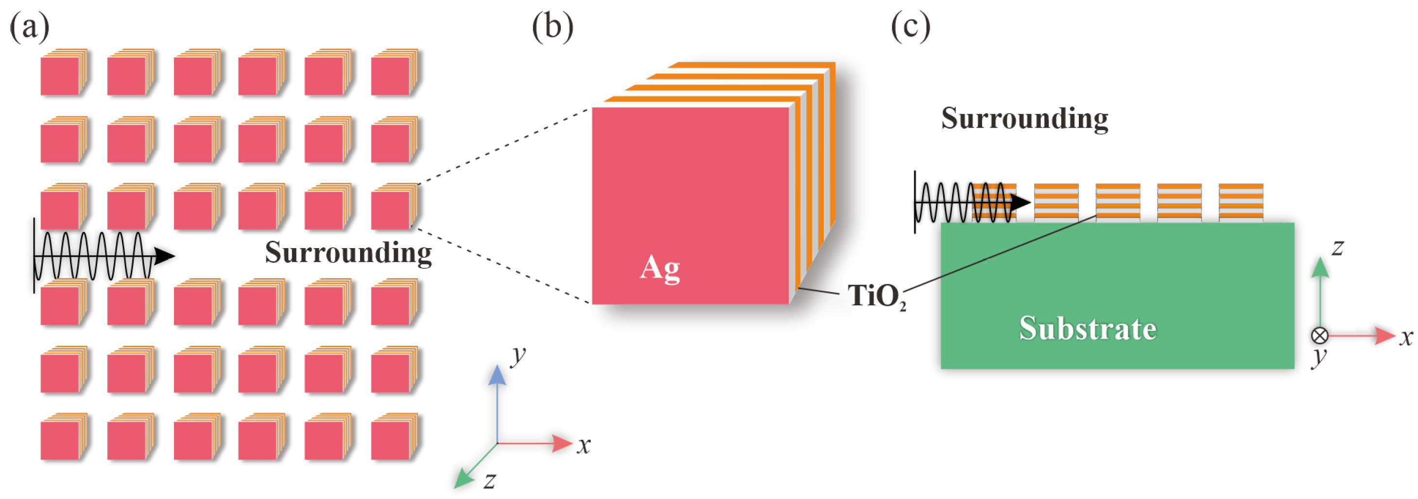
The proposed HMM waveguide consists of arrays of HMM nanorods in a dielectric surrounding environment, as depicted in Figure 1. The HMM arrays form a photonic crystal with a lattice constant of a = 0.2 μm. One array of HMM nanorods is removed to create a line defect, which serves as the waveguide for incident light. Each HMM nanorod has a side length of r = 0.1 μm and is composed of Ag and TiO2 layers, with a thickness of dm = 10 nm and dd = 15 nm, respectively. There are eight layers in every HMM nanorod, with a filling fraction (of metal) of f = 0.4. The effectiveness of the effective medium theory persists even when dealing with eight layers within an HMM rod. This validity is established through rigorous full electromagnetic calculations. We employed two distinct setups for this verification. Firstly, we configured HMM rods with multiple layers and utilized COMSOL’s eigenvalue solver to conduct comprehensive electromagnetic calculations. Secondly, we considered a bulk HMM rod with the incorporation of effective permittivity. Remarkably, our findings reveal that the approximated approach yields results that closely resemble those obtained through full electromagnetic calculations [44]. Numerical studies on the HMM arrays have been conducted using both the plane-wave expansion method and finite-element method, with the commercial software COMSOL Multiphysics (Version 4.2.1.134, CnTech Co., Ltd., Gumi-si, Gyeongsangbuk-do, Republic of Korea). The benefits of employing the plane-wave expansion method and FEM in numerical investigations lie in their direct solution of Maxwell’s equations, yielding highly accurate results that closely mirror real-world scenarios. The plane-wave expansion method is specifically tailored to address electromagnetic challenges within periodic systems. Meanwhile, we employ the FEM to compute light transmission, as well as to assess sensitivity and FOM. The study only considers TE waves with Ez polarization, and as shown in the figure, the light waves propagate in the x-y plane. The transverse and longitudinal components of the effective permittivity of HMMs are denoted as and , respectively. The tensor employed is as follows:
where the off-diagonal elements are zero. The reason for these off-diagonal elements being zero stems from our choice of coordinates aligned with the orientation of the HMM rods, where wave propagation occurs exclusively within the x-y plane. Consequently, the tensor exhibits zero off-diagonal elements in this coordinate system. It is important to note that if an alternate coordinate system is applied, in which wave propagation deviates from the x-y plane, the off-diagonal elements of the tensor will no longer remain zero. In Ez polarization, we have and . The fabrication of the system can be achieved using electron beam lithography, a technique that is widely used to fabricate arrays of nanorods [43]. Compared to conventional HMM-enhanced SPR sensors based on fibers, the proposed waveguide is easier to fabricate as it lies on a planar substrate. In contrast to other waveguide structures, the proposed HMM PtC waveguides exhibit superior performance, especially when it comes to achieving high FOMs. However, they come with increased fabrication complexity, necessitating additional steps involving electron beam lithography to attain the PtC structure. Nonetheless, given the promisingly high FOMs, the HMM PtC waveguide holds the potential for broader applications beyond traditional HMM sensors.
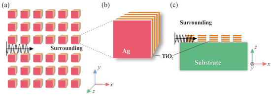
Figure 1.
Schematic diagrams of (a) the HMM PtC waveguide, and (b) the HMM nanorod composed of alternating layers of Ag and TiO2. (c) A detailed cross-sectional view of the HMM PtC waveguide.
To ensure universality, we utilized the Drude model to describe the permittivity of Ag, while representing the refractive index of TiO2 with a constant (nTiO2 = 2.0951), which corresponds to the optical constant of TiO2 at the wavelength of 0.8 μm. The waveguide system was placed on a glass substrate with an optical constant of nglass = 1.440. The permittivity of Ag was obtained using the Drude model as follows:
where , , and are the high-frequency permittivity, the plasma angular frequency, the damping term, and the operating frequency, respectively. The parameters in Equation (2) were derived from experimental data of the permittivity of Ag [45,46] through data fitting, resulting in: = 1.4447, = 1.328 × 10¹⁶ rad/s and = 9.1269 × 10¹³ rad/s. The permittivity of Ag obtained from Drude model fits the experimental data very well.
In Equation (2), the imaginary part of Ag contributes significantly to the loss of wave propagation in the system. The alteration of the SRI causes a change in the electric field distribution, ultimately affecting the absorption of waves by the HMM waveguide. Propagating waves through a bulk Ag or HMM material is challenging due to high material loss and wave vector mismatch, which cannot satisfy the boundary conditions. However, the use of HMM arrays as a photonic crystal (PtC) can overcome this limitation and provide an effective waveguide system. In other words, waves encounter significant absorption challenges within bulk Ag or HMM materials due to the potential for substantial absorption. However, HMM PtC structures are adept at overcoming these obstacles by introducing a bandgap. Within the PtC, wave propagation primarily occurs through the line-defect waveguide, rather than within the bulk HMMs. This configuration mitigates material absorption, all while ensuring strong coupling between SPRs and waveguide modes. The HMM PtC nanostructure system preserves the field enhancement properties of HMM while enabling efficient wave propagation [47]. Moreover, the HMM waveguide system offers flexibility in parameters, which is plausible for various applications.
Since the thickness of the layers inside an HMM rod is much smaller than the wavelength of waves that propagate in the system, the optical property of HMM nanorods can be investigated using effective medium methods. According to the method, an HMM can be treated as having an isotropic permittivity tensor, with components and given by the following equations:
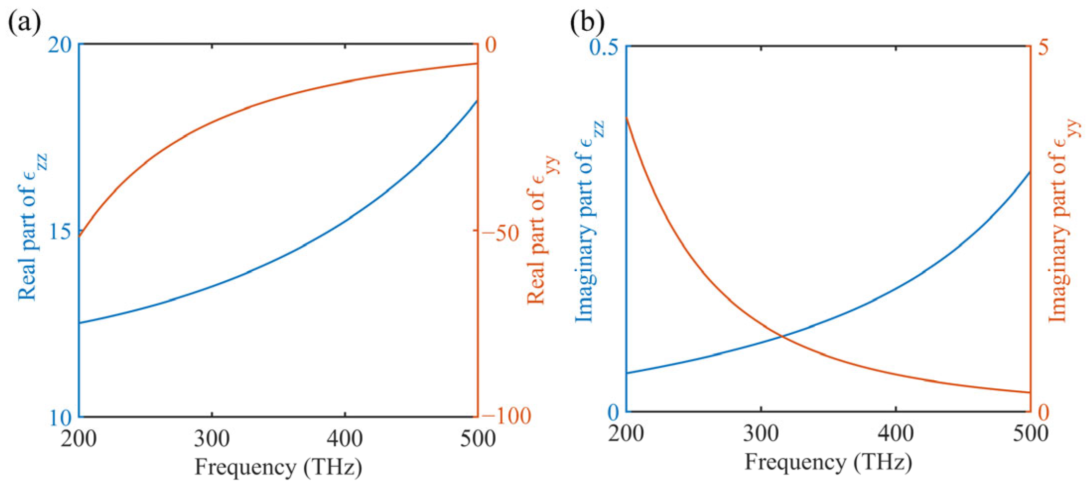
where and are the permittivities of Ag and TiO2, respectively. Using Equations (3) and (4), we calculated the effective permittivity of the HMM as illustrated in Figure 2. By altering the components or fractions of the HMM’s materials, we can adjust its optical properties. Based on the signs of and , we can categorize HMMs as (i) Effective Dielectric (, ), (ii) Effective Metal (, ), (iii) Type-I HMM (, ), and (iv) Type-II HMM (, ). The transition between these HMM types is an important area of inquiry in HMM research, as the different types of HMMs can exhibit unique wave propagation properties.
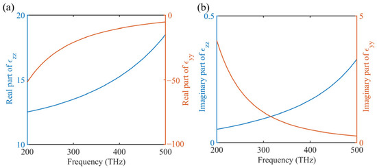
Figure 2.
The longitudinal and transverse components of the effective permittivity ( and ) of the HMMs. The real and imaginary parts of the permittivity are illustrated in panels (a) and (b), respectively.
In Figure 2, when the incident light’s operating frequency falls between 200 THz and 500 THz, the real part of the transverse components of the effective permittivities of HMMs is positive, while the real part of the longitudinal components is negative. This signifies that the HMMs are functioning as Type-I HMM. However, the signs of the components are not important for our waveguide system as long as there are gaps in the PtC structure, which means that the waveguide can operate properly. The dispersion relation shown in the figure is the mainstay for the sensor. As shown in the figure, the effective permittivity of the HMMs changes with the frequency, allowing the HMMs to enhance the sensitivity of the waveguide system. Note that the dispersion relation can be improved further by moving to a frequency region near the transition point of the HMMs, as the dispersion curve changes dramatically. However, the material loss (associated with the imaginary part of permittivity) is also high near the transition point. Therefore, additional optimization is required to balance the two factors that affect the waveguide system’s sensing performance. Overall, the dispersion of HMMs enhances the system’s sensitivity and provides additional versatility when adjusting its properties, making it an ideal platform for realizing high-performance sensors.
Now, let us delve into how the proposed system manages potential errors or discrepancies in the fabrication process. Since the PtC waveguide system operates as an integrated whole, localized disruptions do not significantly impact its overall properties. Consequently, when errors occur, alterations may manifest in local structures, potentially leading to mismatches during wave propagation within the waveguide system. Such mismatches can introduce increased loss in guided modes, modestly affecting the sensor’s efficiency. However, given that a bandgap can be generated across a broad spectrum of PtC structure parameters, and as long as this bandgap remains present and the operating frequency falls within its bounds, inconsistencies will not exert any substantial influence on the waveguide system.
3. Results and Discussions
Figure 3a shows the band structure of the two-dimensional arrays of HMMs with an SRI of 1.33. The bands were computed using COMSOL Multiphysics software based on the finite-element method. Since the structure is periodic, only one column was required to complete the calculation. The selection of simulation parameters adheres to several key criteria. Firstly, the operating frequency is chosen to ensure the presence of a bandgap, the formation of waveguide modes, and the attainment of satisfactory propagation efficiency. Additionally, it is imperative that the frequency of SPR coincides with that of the guided modes. To achieve this alignment, the HMM must effectively behave as a metal in the Ez polarization. These parameters offer the flexibility to modify the sensor’s properties, with room for further optimization. However, the proposed parameter configuration is sufficient to demonstrate the unique characteristics of the HMM PtC waveguide sensor and its exceptional performance. The obtained bands reveal a bandgap between the first and second band, within which a dispersion curve arises. This curve corresponds to the guided modes in the system. The lower cutoff frequency of the guided mode is approximately 345 THz, which marks the lower end of the dispersion curve. By adjusting the SRI, the cutoff frequency can be varied. In Figure 3b, the electric field (Ez) profiles of the guided modes are depicted for kx = 0, 0.1(2π/a), and 0.2(2π/a), while ky = 0. The field profiles indicate the localization of the guided modes in the y direction. Note that in such a system, only a single guided mode can be supported. To achieve multi-mode operation, one can expand the line defect between the HMM arrays by removing more rows of HMM nanorods.
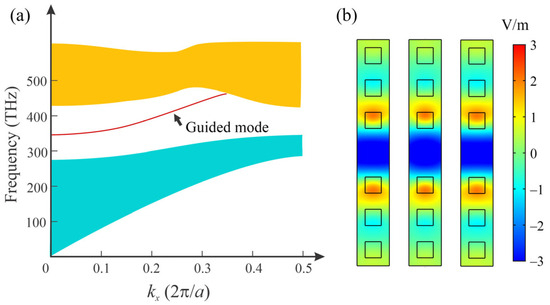
Figure 3.
(a) Band structure of the HMM PtC waveguide when SRI = 1.33, with an arrow highlighting a dispersion curve of the guided mode located in the middle of the bandgap. (b) Electric field (Ez) profiles of guided modes for different values of kx (0, 0.1(2π/a), and 0.2(2π/a)) while ky is fixed at 0. The eigenfrequencies for these modes are 344.38 THz, 356.07 THz, and 390.22 THz, respectively.
Based on the calculation result, all the eigenfrequencies have imaginary parts, which are not shown in the figure. The existence of imaginary parts in the eigenfrequencies indicates that all the modes will experience losses over time and their amplitude will decrease. These losses are mainly caused by the material loss of Ag. Moreover, changing the SRI will have an impact on both the imaginary and real parts of the guided modes, represented as and , respectively. If the waveguide is long enough, the transmission spectra of the sensor can be obtained using the following equation:
where is the transmission power, is the angular frequency of the light source, and L is the length of the HMM waveguide. The working mechanism of conventional sensors typically follows Equation (5). However, in our work, the change in SRI not only modifies the output of Equation (5) but also causes the dispersion curve to change, leading to a further modification of the transmission spectra. This is where the HMM waveguide sensors have an advantage over conventional ones. In the subsequent discussion, we will provide a detailed explanation of how the transmission spectra of the system are affected by the change in SRI. Note that the material loss of Ag is exceptionally low for several reasons. Firstly, the system operates in a state where waves primarily propagate within the waveguide, rather than traversing the bulk HMM. In theory, evanescent waves, which are prevalent in this scenario, do not transport energy, resulting in minimal absorption. Additionally, the system employs a limited-size PtC structure, further reducing Ag’s material loss.
In the simulation presented above, we focused only on a two-dimensional model and neglected the substrate. We have confirmed that this model is accurate enough for our proposal by investigating the field distribution in the third dimension. Figure 4 shows the electric field (Ez) profiles in x-y and x-z planes from simulations using a three-dimensional model. The model employed the same parameters for the HMM arrays as shown in Figure 3, and the HMM nanorods have a thickness of 0.1 μm. The field profiles demonstrate that the field can be localized in both the y and z directions without divergence. This result indicates that the standing wave condition can be achieved in the third dimension for the HMM waveguide system. Furthermore, additional simulations have confirmed that we can use a substrate material with the same refractive index as the SRI, and the guided mode can still propagate effectively within the waveguide without diffusion. These results demonstrate that the proposed sensor can be both compact and flexible, as the structure can be fabricated on a variety of substrates and still function properly. Additionally, the results suggest that the design of the sensor can be simplified by considering a 2D system instead of a 3D one.
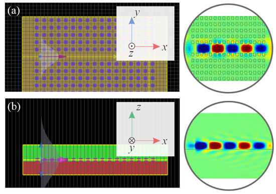
Figure 4.
The result of a three-dimensional simulation, which illustrates the electric field (Ez) profiles of the guided mode in both the (a) x-y plane and (b) x-z planes. The simulation highlights the localization of the electric field in the y and z directions, as the electric field appears to be concentrated in these two directions. Notably, the frequency of the incident light in this simulation is 360 THz.
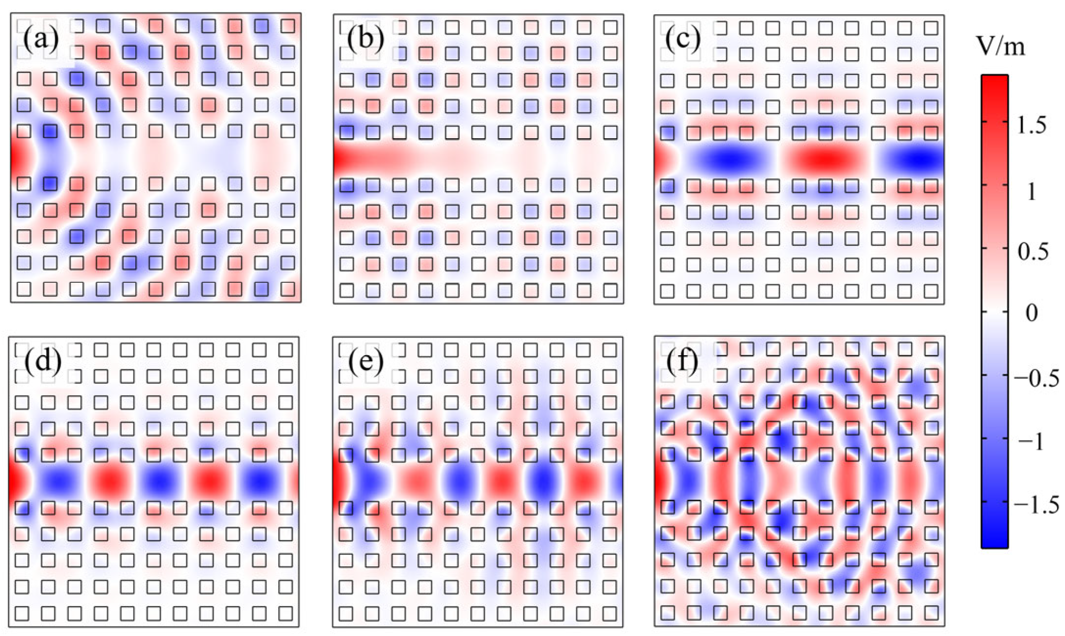
For different frequencies of the incident light, the waveguide indicates different properties in the guidance of waves, as shown in Figure 5. In total, 11 columns of HMM nanorods are used in Figure 5, so the total length of the waveguide is 2.2 μm. As shown in Figure 5a, when the frequency of the incident light is 325 THz, which falls in the first band and is below the cutoff frequency, the propagation of light indicates non-localization and no guided modes exist. As a result, little energy has passed through the waveguide to the right end. In Figure 5b, the frequency of the incidence is 350 THz, which falls in the gap and is below the cutoff frequency, we can clearly see that the field decays exponentially. The HMM waveguide is in a “cutoff” state, blocking the forward propagation of waves. Additionally, near the cutoff frequency, the guided modes have very small wave vectors and low group velocities, e.g., the group velocity is approaching zero at the frequency of 345 THz. Therefore, only a small amount of energy from the incident light can successfully propagate toward the other end of the waveguide. Note that some of the energy of the incident light also has been absorbed by the HMM nanorods. At the frequencies of 375 THz and 425 THz, the wave can propagate in the waveguide to the other end, but their transmissions are different, which is related to the property of the waveguide in different frequencies. All the phenomena above can be explained by the dispersion curve shown in the band structure in Figure 3. Consequently, modifying the dispersion curve means changing the propagation behavior of waves in the HMM waveguide. The key benefit of utilizing the HMM PtC waveguide is its capacity to enhance the FOM in comparison to conventional SPR sensors. This advantage is rooted in its ability to yield high-performance sensors. FOM serves as a critical parameter that characterizes sensing efficacy, in which a higher FOM equates to greater sensitivity when it comes to detecting even minute changes in the surroundings. These advantages hold profound implications in real-world applications.
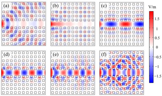
Figure 5.
The electric field (Ez) profiles of waves propagating in the HMM PtC waveguide under different frequencies of incident light. Specifically, panels (a–f) depict the Ez profiles when the incident light frequencies are 325 THz, 350 THz, 375 THz, 425 THz, 450 THz, and 500 THz, respectively.
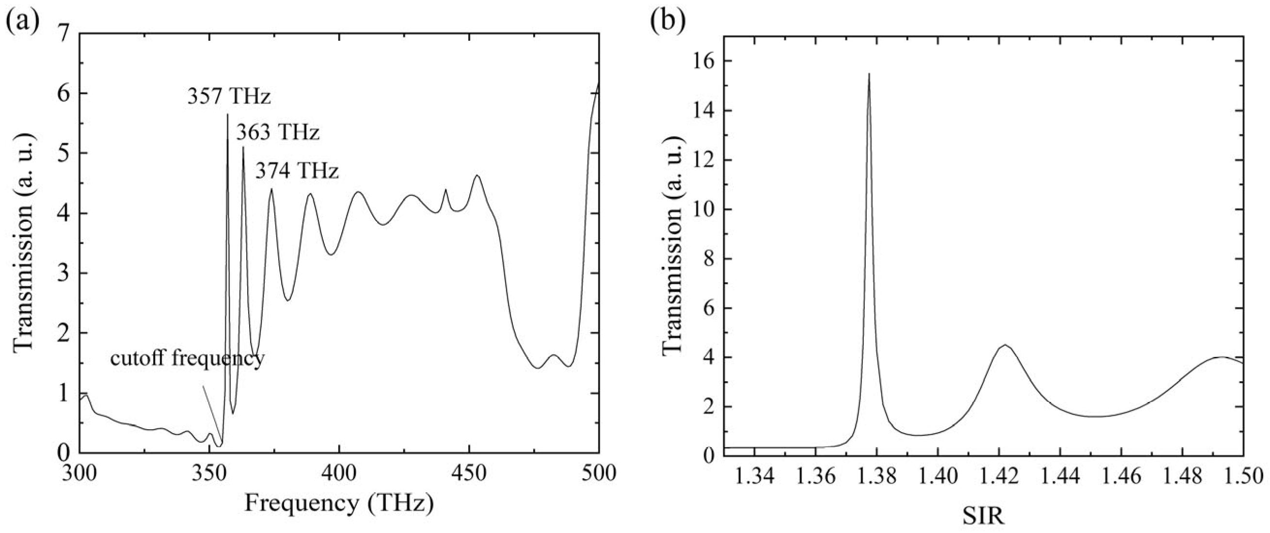
The full transmission spectrum is illustrated in Figure 6a, from which we can accurately determine the cutoff frequency of the waveguide to be approximately 355 THz. Below this frequency, the waveguide has very low transmission, as the incident light is either blocked due to the gap or undergoes diffusion propagation within the band. When the waveguide is working above the cutoff frequency, guided modes are generated, resulting in high transmission of the waveguide. The multiple peaks in the spectrum correspond to frequencies that satisfy the resonant condition of the Fabry–Perot (FP) cavity. The FP cavity is formed by the finite length of the waveguide, with the two ends of the waveguide functioning as reflectors. These transmission peaks are crucial for achieving sensors with high FOMs. To illustrate this point, we set the frequency of the incident light to 350 THz and obtained the transmission of the HMM waveguide at different SIRs, as shown in Figure 6b. Two factors play important roles in the propagation of light: the change in the dispersion curve of the guided mode following the change in the propagation behavior of light, and the energy absorbed by the materials, which reduces the transmission power of the waveguide. Modification of the SIR affects both of these factors, which is how the sensor operates. Figure 6b shows that the sensing ability of the HMM PtC waveguide is excellent, with a significant change in transmission, particularly when the SIR is around 1.370 or 1.380. For example, when the SIR increases from 1.373 to 1.377, the transmission increases from 1.144 to 13.832, which represents a one-order-of-magnitude increase in transmission.
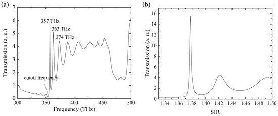
Figure 6.
(a) The transmission spectrum of the HMM PtC waveguide when the SIR is 1.33. (b) The transmission of the HMM PtC waveguide when the frequency of the incident light is 350 THz.
Conventional waveguides exhibit a theoretical red shift in their entire transmission spectrum as the SIR increases, but the effect is too small to be practically applicable. On the other hand, the HMM PtC waveguide has been improved through the combined effects of the dispersion properties of HMMs and PtCs. As a result, the nonlinear effect is considerably prominent. The sensitivity of the HMM PtC waveguide sensor (S) can be defined as:
where is the shift in the wavelength, is the shift in the angular frequency, and is the change in the SIR. Furthermore, the FOM of the system can be calculated using the following equation:
where FWHM (full width at half-maximum) refers to the width of the transmission spectra of the HMM PtC waveguide sensor, measured at the point at which the transmission reaches half of its maximum value. By utilizing the FEM, we can compute the transmission spectrum. By adjusting various parameters within the model, such as altering the refractive index of the surrounding materials, we can obtain spectra under these conditions. Subsequently, we can calculate variables like (the shift in wavelength), (the shift in angular frequency), and (the change in SIR). With these values in hand, we can then proceed to calculate sensitivity using Equation (6). Similarly, the FOM is determined using the same methodology.
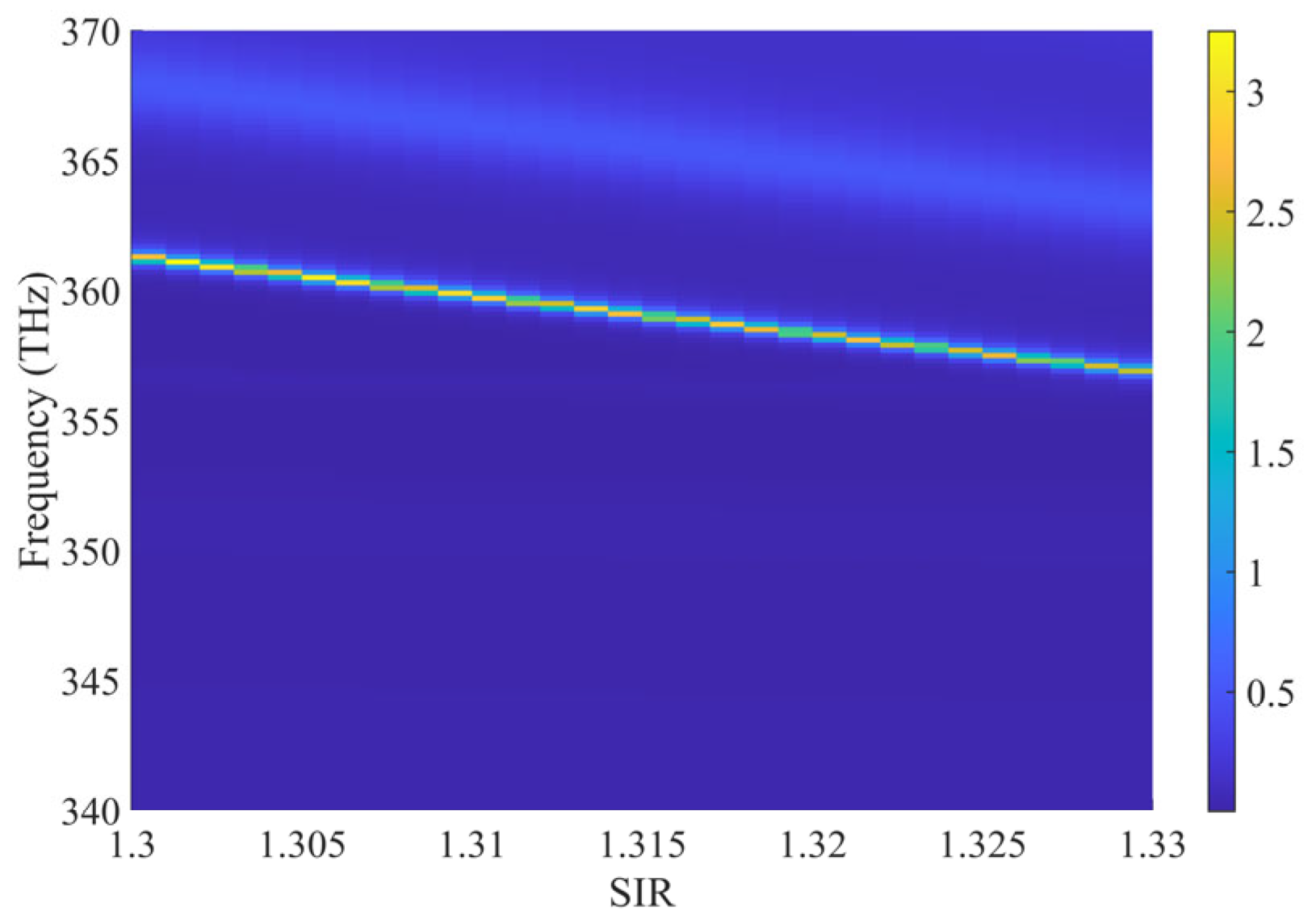
Figure 7 illustrates a more detailed relationship between transmission, frequency, and SIR. The y-axis shows the transmission spectra for different SIRs, with two transmission peaks near 360 THz and 365 THz. Along the x-axis, as the SIR increases, the transmission peaks move to lower frequencies, and the whole transmission spectrum is red-shifted. According to the results, the average sensitivity and FOM of the HMM PtC waveguide sensor around 360 THz can be calculated based on Equations (6) and (7), respectively, which are 476.10 nm/RIU (RIU: refractive index unit) and 476.10 RIU−1. The sensitivity appears to be nonsignificant compared to that of conventional SPR sensors. However, we only use a waveguide with a length of 0.8 μm here, which is much shorter than the centimeter-scale lengths of conventional SPR sensors. The longer the waveguide, the greater the sensitivity will be, since the absorption will be more significant. On the other hand, the FOM of the HMM PtC waveguide sensor is very promising compared to conventional sensors. Usually, only resonant cavities can provide such large FOMs, but cavities are not suitable for sensing because the area of SIR for sensing is too small, requiring very precise fabrication. Table 1 shows a comparison of different types of sensors. After comparing the performance of the HMM PtC waveguide sensor with conventional fiber sensors, it is evident that the former has a much larger FOM and is therefore superior in sensing. Although conventional fiber sensors have high sensitivity, their small FOM limits their performance. For example, changing the SIR at a specific frequency may not significantly modify the transmission due to the large FWHM of the sensors. The drawback can be addressed by attaining higher FOMs using an alternative configuration, such as the HMM PtC waveguide. Indeed, the utilization of the guided modes in HMM waveguides allows for the direct coupling of electromagnetic waves to the highly dispersive material, making it a more efficient method than the side-coupling of fiber modes to SPR modes. Additionally, while fabrication presents greater challenges, the scalability of the proposed sensor outshines conventional fibers, especially within integrated optic systems. Although fabrication costs are high, maintenance costs remain low. Moreover, once the complexity hurdle has been addressed, the proposed sensor can outperform other state-of-the-art sensors.

Figure 7.
The transmission of the HMM PtC waveguide in different frequencies and SIRs.

Table 1.
Comparison of different types of sensors.
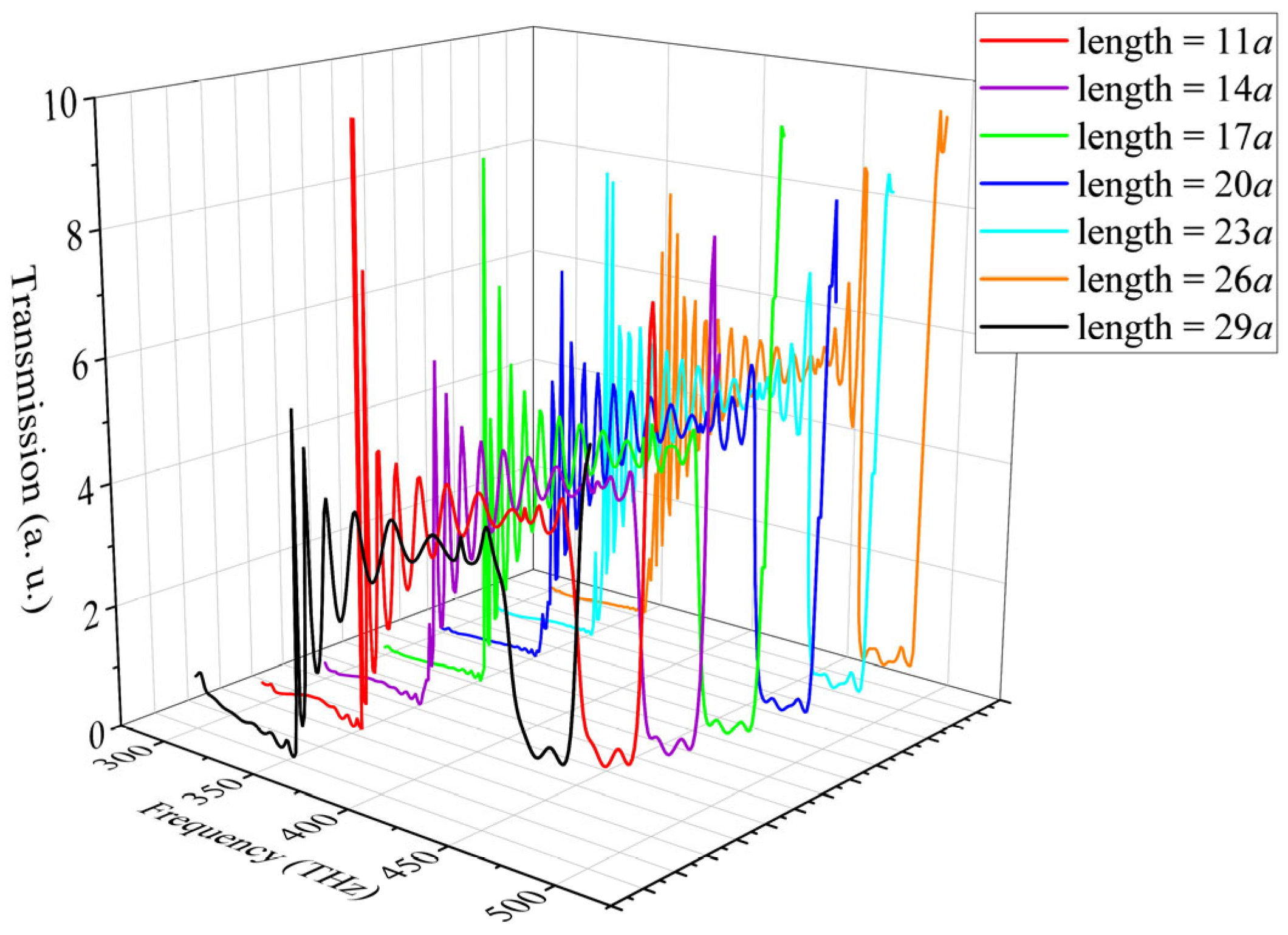
The HMM PtC waveguide sensor can be designed with various lengths to suit different applications. Figure 8 shows the calculated transmission spectra of HMM PtC waveguides with different lengths, which exhibit similar properties. This confirms that the configuration is very flexible and can be applied to various scenarios. Additionally, the HMM PtC waveguide sensor is both compact and efficient. Note that the operational wavelength of the suggested sensor is adjustable [51]. Altering the structural parameters can lead to modifications in the transmission spectrum of the HMM PtC waveguide. The operational wavelength of our proposed sensor can be finely tuned by adjusting the parameters of the HMM rods. The HMM PtC waveguide sensor holds substantial potential for diverse applications. Tailoring the refractive indices of the surrounding materials to match the sensor’s specific application is a key feature. For instance, in temperature sensing applications, thermal infrared materials can be employed as the surrounding medium. As the temperature fluctuates, the refractive index of the surrounding material dynamically changes, influencing the waveguide modes and, subsequently, absorption and transmission properties. This adaptability allows seamless integration and offers a high FOM, making it suitable for a wide range of scenarios. Furthermore, it is expected to meet various requirements with ease.

Figure 8.
The transmission spectra of the HMM PtC waveguide with various lengths.
4. Conclusions
In summary, our study presents a novel approach for developing high FOM sensors using HMM PtC waveguides. Compared to conventional HMM sensors, the HMM PtC waveguide sensor employs an innovative approach that combines both HMM and PtC structures. This integration facilitates the direct coupling of SPRs with guided modes, resulting in exceptionally high efficiency and a substantial FOM. While the fabrication process may be more complex and costly compared to conventional sensors, the outstanding performance of the HMM PtC sensor justifies these investments. By utilizing the HMM arrays as waveguides, the unique properties of HMM can be fully harnessed to achieve optimal sensor performance. Through numerical simulations, we have demonstrated that our proposed sensor design exhibits a sensitivity of 324.16 nm/RIU and an exceptional FOM of 469.58 RIU−1, surpassing what is currently achievable with conventional HMM sensors, which only have low FOMs. Note that the sensitivity and FOM calculations were performed using FEM, where both the layer parameters of the HMM and the lattice parameters of the PtC structure played pivotal roles in determining the results.
Our work offers promising opportunities for advancing the performance of HMM sensors, with potential applications in biology, medicine, and clinical settings. This sensor has the capability to detect changes when the surrounding materials are altered. Moreover, it is noteworthy that the HMM PtC waveguide sensor can be miniaturized and seamlessly integrated, rendering it highly competitive in the fields of biology and clinical applications. One potential challenge lies in the demanding fabrication techniques required to construct the sensor, but this challenge is expected to be mitigated as technology continues to advance. Due to its compact design, the HMM PtC waveguide sensor can be seamlessly integrated into photonic chips. Furthermore, the PtC platform offers considerable scalability. The potential challenges associated with this system primarily revolve around fabrication. However, the solutions to these challenges are feasible and involve additional operations and efforts, which are not particularly complex tasks.
The FEM employed in this manuscript can exclusively provide static results. This limitation arises from the inherent nature of FEM as a numerical technique operating in the frequency domain. In instances in which nonlinear effects are essential to the system, FEM fails to deliver the desired results. In such cases, a transition to time-domain solutions becomes imperative, necessitating the utilization of the Finite-Difference Time-Domain (FDTD) method.
Future research and development in this field encompass two key aspects. The first is the advancement of fabrication technology, which aims to address the challenges associated with achieving greater precision when constructing both HMM and PtC structures. The second is the exploration of the unique phenomena within the HMM PtC system. The synergy resulting from combining these two exemplary structural designs offers the potential to unlock innovative solutions for the development of high-performance photonic devices.
Author Contributions
Conceptualization, Y.Z. and Q.W.; methodology, Y.Z.; software, Y.Z.; validation, F.K., B.A. and Q.W.; formal analysis, Y.Z.; investigation, Y.Z., F.K., B.A. and Q.W.; resources, Y.Z.; data curation, Q.W.; writing—original draft preparation, Y.Z., F.K. and B.A.; writing—review and editing, Y.Z., F.K., B.A. and Q.W.; visualization, Y.Z.; supervision, Q.W.; project administration, Q.W.; funding acquisition, Y.Z. and Q.W. All authors have read and agreed to the published version of the manuscript.
Funding
The authors would like to extend their heartfelt thanks for the support provided by the China Postdoctoral Science Foundation (No. 2023M732734) and the Shenzhen Science and Technology Project (No. JCYJ20190808161801637), which were essential for the successful completion of this work.
Data Availability Statement
The data presented in this study are available on request from the corresponding author.
Conflicts of Interest
The authors declare no conflict of interest.
References
- Estakhri, N.M.; Edwards, B.; Engheta, N. Inverse-designed metastructures that solve equations. Science 2019, 363, 1333–1338. [Google Scholar] [CrossRef]
- Lalegani, Z.; Seyyed Ebrahimi, S.A.; Hamawandi, B.; La Spada, L.; Batili, H.; Toiprak, M.S. Targeted dielectric coating of silver nanoparticles with silica to manipulate optical properties for metasurface applications. Mater. Chem. Phys. 2022, 287, 126250. [Google Scholar] [CrossRef]
- Pacheco-Peña, V.; Beruete, M.; Rodríguez-Ulibarri, P.; Engheta, N. On the performance of an ENZ-based sensor using transmission line theory and effective medium approach. New J. Phys. 2019, 21, 043056. [Google Scholar] [CrossRef]
- Akbari, M.; Shahbazzadeh, M.J.; Spada, L.; Khajehzadeh, A. The graphene field effect transistor modeling based on an optimized ambipolar virtual source model for DNA detection. Appl. Sci. 2021, 11, 8114. [Google Scholar] [CrossRef]
- Greybush, N.J.; Pacheco-Peña, V.; Engheta, N.; Murray, C.B.; Kagan, C.R. Plasmonic optical and chiroptical response of self-assembled Au nanorod equilateral trimers. ACS Nano 2019, 13, 1617–1624. [Google Scholar] [CrossRef]
- Lincoln, R.L.; Scarpa, F.; Ting, V.P.; Trask, R.S. Multifunctional composites: A metamaterial perspective. Multifunct. Mater. 2019, 2, 043001. [Google Scholar] [CrossRef]
- Poddubny, A.; Iorsh, I.; Belov, P.; Kivshar, Y. Hyperbolic metamaterials. Nat. Photonics 2013, 7, 948–957. [Google Scholar] [CrossRef]
- Gric, T.; Hess, O. Investigation of hyperbolic metamaterials. Appl. Sci. 2018, 8, 1222. [Google Scholar] [CrossRef]
- Bhardwaj, A.; Srivastava, K.V.; Ramakrishna, S.A. Enhanced coupling of light from subwavelength sources into a hyperbolic metamaterial fiber. J. Light. Technol. 2019, 37, 3064–3072. [Google Scholar] [CrossRef]
- Davidovich, M.V. Hyperbolic metamaterials: Production, properties, applications, and prospects. Phys. Uspekhi 2019, 62, 1173. [Google Scholar] [CrossRef]
- Huo, P.; Zhang, S.; Liang, Y.; Lu, Y.; Xu, T. Hyperbolic metamaterials and metasurfaces: Fundamentals and applications. Adv. Opt. Mater. 2019, 7, 1801616. [Google Scholar] [CrossRef]
- Cortes, C.; Newman, W.; Molesky, S.; Jacob, Z. Quantum nanophotonics using hyperbolic metamaterials. J. Opt. 2012, 14, 063001. [Google Scholar] [CrossRef]
- Popov, A.K.; Myslivets, S.A.; Slabko, V.V.; Tkachenko, V.A.; George, T.F. Shaping light in backward-wave nonlinear hyperbolic metamaterials. Photonics 2018, 5, 8. [Google Scholar] [CrossRef]
- Liu, J.; Chen, W.; Ma, W.-Z.; Chen, Y.-S.; Deng, X.-C.; Zhuang, P.-P.; Ye, Q. Biaxial hyperbolic metamaterial THz broadband absorber utilizing anisotropic two-dimensional materials. Results Phys. 2021, 22, 103818. [Google Scholar] [CrossRef]
- Wang, Z.; Huo, Y.; Ning, T.; Liu, R.; Zha, Z.; Shafi, M.; Li, C.; Li, S.; Xing, K.; Zhang, R.; et al. Composite structure based on gold-nanoparticle layer and HMM for surface-enhanced Raman spectroscopy analysis. Nanomaterials 2021, 11, 587. [Google Scholar] [CrossRef]
- Feng, K.; Sivco, D.L.; Hoffman, A.J. Engineering optical emission in sub-diffraction hyperbolic metamaterial resonators. Opt. Express 2018, 26, 4382–4391. [Google Scholar] [CrossRef]
- Azmoudeh, E.; Farazi, S. Ultrafast and low power all-optical switching in the mid-infrared region based on nonlinear highly doped semiconductor hyperbolic metamaterials. Opt. Express 2021, 29, 13504–13517. [Google Scholar] [CrossRef]
- Jiang, H.-L.; Pan, J.; Zhou, W.; Li, H.-M.; Liu, S. Fabrication and application of arrays related to two-dimensional materials. Rare Met. 2022, 41, 262–286. [Google Scholar] [CrossRef]
- Mitsushio, M.; Higashi, S.; Higo, M. Construction and evaluation of a gold-deposited optical fiber sensor system for measurements of refractive indices of alcohols. Sens. Actuators A Phys. 2004, 111, 252–259. [Google Scholar] [CrossRef]
- Pollet, J.; Delport, F.; Janssen, K.P.; Jans, K.; Maes, G.; Pfeiffer, H.; Wevers, M.; Lammertyn, J. Fiber optic SPR biosensing of DNA hybridization and DNA–protein interactions. Biosens. Bioelectron. 2009, 25, 864–869. [Google Scholar] [CrossRef]
- Herranz, S.; Bocková, M.; Marazuela, M.D.; Homola, J.; Moreno-Bondi, M.C. An SPR biosensor for the detection of microcystins in drinking water. Anal. Bioanal. Chem. 2010, 398, 2625–2634. [Google Scholar] [CrossRef]
- Caucheteur, C.; Voisin, V.; Albert, J. Near-infrared grating-assisted SPR optical fiber sensors: Design rules for ultimate refractometric sensitivity. Opt. Express 2015, 23, 2918–2932. [Google Scholar] [CrossRef]
- Skorobogatiy, M.; Kabashin, A. Plasmon excitation by the Gaussian-like core mode of a photonic crystal waveguide. Opt. Express 2006, 14, 8419–8424. [Google Scholar] [CrossRef]
- Kim, S.A.; Kim, S.J.; Moon, H.; Jun, S.B. In vivo optical neural recording using fiber-based surface plasmon resonance. Opt. Lett. 2012, 37, 614–616. [Google Scholar] [CrossRef]
- Zeng, S.; Baillargeat, D.; Ho, H.-P.; Yong, K.-T. Nanomaterials enhanced surface plasmon resonance for biological and chemical sensing applications. Chem. Soc. Rev. 2014, 43, 3426–3452. [Google Scholar] [CrossRef]
- Wang, H.; Zhang, H.; Dong, J.; Hu, S.; Zhu, W.; Qiu, W.; Lu, H.; Yu, J.; Guan, H.; Gao, S.; et al. Sensitivity-enhanced surface plasmon resonance sensor utilizing a tungsten disulfide (WS 2) nanosheets overlayer. Photonics Res. 2018, 6, 485–491. [Google Scholar] [CrossRef]
- Yang, M.; Xiong, X.; He, R.; Luo, Y.; Tang, J.; Dong, J.; Lu, H.; Yu, J.; Guan, H.; Zhang, J.; et al. Halloysite nanotube-modified plasmonic interface for highly sensitive refractive index sensing. ACS Appl. Mater. Interfaces 2018, 10, 5933–5940. [Google Scholar] [CrossRef]
- Vasilantonakis, N.; Nasir, M.E.; Dickson, W.; Wurtz, G.A.; Zayats, A.V. Bulk plasmon-polaritons in hyperbolic nanorod metamaterial waveguides. Laser Photonics Rev. 2015, 9, 345–353. [Google Scholar] [CrossRef]
- Vasilantonakis, N.; Wurtz, G.A.; Podolskiy, V.A.; Zayats, A.V. Refractive index sensing with hyperbolic metamaterials: Strategies for biosensing and nonlinearity enhancement. Opt. Express 2015, 23, 14329–14343. [Google Scholar] [CrossRef]
- Cheng, M.; Fu, P.; Weng, M.; Chen, X.; Zeng, X.; Feng, S.; Chen, R. Spatial and angular shifts of terahertz wave for the graphene metamaterial structure. J. Phys. D Appl. Phys. 2015, 48, 285105. [Google Scholar] [CrossRef]
- Sreekanth, K.V.; Alapan, Y.; ElKabbash, M.; Ilker, E.; Hinczewski, M.; Gurkan, U.A.; De Luca, A.; Strangi, G. Extreme sensitivity biosensing platform based on hyperbolic metamaterials. Nat. Mater. 2016, 15, 621–627. [Google Scholar] [CrossRef]
- Sreekanth, K.V.; Mahalakshmi, P.; Han, S.; Rajan, M.S.M.; Choudhury, P.K.; Singh, R. Brewster Mode-Enhanced Sensing with Hyperbolic Metamaterial. Adv. Opt. Mater. 2019, 7, 1900680. [Google Scholar] [CrossRef]
- Guo, Z.W.; Jiang, H.T.; Li, Y.H.; Chen, H.; Agarwal, G.S. Enhancement of electromagnetically induced transparency in metamaterials using long range coupling mediated by a hyperbolic material. Opt. Express 2018, 26, 627–641. [Google Scholar] [CrossRef]
- Yang, W.; Gao, J.J.; Li, Z.; Li, C.; Cheng, Y.; Huo, Y.; Jiang, S.; Jiang, M. High-performance D-type plastic fiber SPR sensor based on a hyperbolic metamaterial composed of Ag/MgF2. J. Mater. Chem. C 2021, 9, 13647–13658. [Google Scholar] [CrossRef]
- Shalabney, A.; Abdulhalim, I. Sensitivity-enhancement methods for surface plasmon sensors. Laser Photonics Rev. 2011, 5, 571–606. [Google Scholar] [CrossRef]
- Gasior, K.; Martynkien, T.; Napiorkowski, M.; Zolnacz, K.; Mergo, P.; Urbanczyk, W. A surface plasmon resonance sensor based on a single mode D-shape polymer optical fiber. J. Opt. 2016, 19, 025001. [Google Scholar] [CrossRef]
- Sreekanth, K.V.; Alapan, Y.; ElKabbash, M.; Wen, A.M.; Ilker, E.; Hinczewski, M.; Gurkan, U.A.; Steinmetz, N.F.; Strangi, G. Enhancing the angular sensitivity of plasmonic sensors using hyperbolic metamaterials. Adv. Opt. Mater. 2016, 4, 1767–1772. [Google Scholar] [CrossRef]
- Zhao, J.; Cao, S.; Liao, C.; Wang, Y.; Wang, G.; Xu, X.; Fu, C.; Xu, G.; Lian, J.; Wang, Y. Surface plasmon resonance refractive sensor based on silver-coated side-polished fiber. Sens. Actuators B Chem. 2016, 230, 206–211. [Google Scholar] [CrossRef]
- Dong, J.; Zhang, Y.; Wang, Y.; Yang, F.; Hu, S.; Chen, Y.; Zhu, W.; Qiu, W.; Guan, H.; Lu, H.; et al. Side-polished few-mode fiber based surface plasmon resonance biosensor. Opt. Express 2019, 27, 11348–11360. [Google Scholar] [CrossRef]
- Hu, S.; Chen, Y.; Chen, Y.; Chen, L.; Zheng, H.; Azeman, N.H.; Liu, M.X.; Liu, G.-S.; Luo, Y.; Chen, Z. High-performance fiber plasmonic sensor by engineering the dispersion of hyperbolic metamaterials composed of Ag/TiO2. Opt. Express 2020, 28, 25562–25573. [Google Scholar] [CrossRef]
- Hu, S.; Chen, J.; Liang, J.; Luo, J.; Shi, W.; Yuan, J.; Chen, Y.; Chen, L.; Chen, Z.; Liu, G.-S.; et al. Hyperbolic-Metamaterials-Based SPR Temperature Sensor Enhanced by a Nanodiamond-PDMS Hybrid for High Sensitivity and Fast Response. ACS Appl. Mater. Interfaces 2022, 14, 42412–42419. [Google Scholar] [CrossRef]
- Li, J.; Xu, M.; Liu, J.; Li, H.; Song, H.; Zhou, A. Theoretical analysis of a highly sensitive SPR temperature sensor based on Ag/TiO2 hyperbolic metamaterials and PDMS film. Opt. Laser Technol. 2022, 156, 108610. [Google Scholar] [CrossRef]
- Galfsky, T.; Gu, J.; Narimanov, E.E.; Menon, V.M. Photonic hypercrystals for control of light–matter interactions. Proc. Natl. Acad. Sci. USA 2017, 114, 5125–5129. [Google Scholar] [CrossRef]
- Zheng, Y.; Wang, Q.; Lin, M.; Bibbò, L.; Ouyang, Z. Twisted bands with degenerate points of photonic hypercrystals in infrared region. Nanomaterials 2022, 12, 1985. [Google Scholar] [CrossRef]
- Johnson, P.B.; Christy, R.-W. Optical constants of the noble metals. Phys. Rev. B 1972, 6, 4370. [Google Scholar] [CrossRef]
- Popov, V.; Lavrinenko, A.V.; Novitsky, A. Surface waves on multilayer hyperbolic metamaterials: Operator approach to effective medium approximation. Phys. Rev. B 2018, 97, 125428. [Google Scholar] [CrossRef]
- Zheng, Y.; Wang, Q.; Lin, M.; Ouyang, Z. Enhancement of self-collimation effect in photonic crystal membranes using hyperbolic metamaterials. Nanomaterials 2022, 12, 555. [Google Scholar] [CrossRef]
- Zhang, H.; Chen, Y.; Feng, X.; Xiong, X.; Hu, S.; Jiang, Z.; Dong, J.; Zhu, W.; Qiu, W.; Guan, H.; et al. Long-range surface plasmon resonance sensor based on side-polished fiber for biosensing applications. IEEE J. Sel. Top. Quantum Electron. 2018, 25, 2868159. [Google Scholar] [CrossRef]
- Shukla, S.; Sharma, N.K.; Sajal, V. Sensitivity enhancement of a surface plasmon resonance based fiber optic sensor using ZnO thin film: A theoretical study. Sens. Actuators B Chem. 2015, 206, 463–470. [Google Scholar] [CrossRef]
- Huang, T. Highly Sensitive SPR Sensor Based on D-shaped Photonic Crystal Fiber Coated with Indium Tin Oxide at Near-Infrared Wavelength. Plasmonics 2017, 12, 583–588. [Google Scholar] [CrossRef]
- Abdulkareem, M.-U.A.; López-Rayón, F.; Sosa-Sánchez, C.T.; Bautista González, R.E.; Arroyo Carrasco, M.L.; Peña-Gomar, M.; Coello, V.; Téllez-Limón, R. Integrated Optical Filters with Hyperbolic Metamaterials. Nanomaterials 2023, 13, 759. [Google Scholar] [CrossRef]


Disclaimer/Publisher’s Note: The statements, opinions and data contained in all publications are solely those of the individual author(s) and contributor(s) and not of MDPI and/or the editor(s). MDPI and/or the editor(s) disclaim responsibility for any injury to people or property resulting from any ideas, methods, instructions or products referred to in the content. |
© 2023 by the authors. Licensee MDPI, Basel, Switzerland. This article is an open access article distributed under the terms and conditions of the Creative Commons Attribution (CC BY) license (https://creativecommons.org/licenses/by/4.0/).