Abstract
In this study, the results of hydrogen plasma treatments of β-Ga2O3, α-Ga2O3, κ-Ga2O3 and γ-Ga2O3 polymorphs are analyzed. For all polymorphs, the results strongly suggest an interplay between donor-like hydrogen configurations and acceptor complexes formed by hydrogen with gallium vacancies. A strong anisotropy of hydrogen plasma effects in the most thermodynamically stable β-Ga2O3 are explained by its low-symmetry monoclinic crystal structure. For the metastable, α-, κ- and γ-polymorphs, it is shown that the net result of hydrogenation is often a strong increase in the density of centers supplying electrons in the near-surface regions. These centers are responsible for prominent, persistent photocapacitance and photocurrent effects.
1. Introduction
Ga2O3 is a wide-bandgap semiconductor material currently under intense study for a new generation of ultra-high-power electronic devices and high-performance UV solar-blind photodetectors [1,2,3,4]. As with some other wide-bandgap semiconductors, Ga2O3 is characterized by prominent polymorphism. Hydrogen is one of the most important impurities in this material. Interstitial hydrogen (Hi) and hydrogen at the oxygen site (HO) are predicted to be shallow donors. One of the most important interactions is with gallium vacancies (VGa) to form VGa-H complexes, since these have especially low formation energies. This H can have strong impacts on the electrical conductivity.
Six different polymorphs of Ga2O3 have been described in the literature, with four being of practical interest: thermodynamically stable monoclinic β-Ga2O3 and three metastable polymorphs, (1) corundum α-Ga2O3, (2) orthorhombic κ-Ga2O3 and (3) the cubic γ-Ga2O3 with defect spinel structure [1,2]. The main focus has been on β-Ga2O3, which, in addition to the wide bandgap of 4.7–4.9 eV and a high breakdown electric field of at least 8 MV/cm (several times higher than that for SiC or GaN), has an advantage, namely, that it can be grown in bulk crystal form using standard melt-growth techniques. This contrasts with the physical vapor transport technique needed for SiC crystals, meaning that the cost of growing bulk substrates is less for Ga2O3. β-Ga2O3 can be easily doped n-type with an electron concentration from mid-1015 to ~1019 cm−3 or made semi-insulating by doping with Fe, Mg or N. It can be grown epitaxially by all versions of epitaxial growth and has convenient ternary solid solutions with Al2O3 and In2O3, allowing the fabrication of useful heterojunction devices [2,4]. Various devices, such as high-power rectifiers, field-effect transistors (FETs), vertical FETs of different designs and heterojunction high-electron-mobility transistors (HEMTs) with promising properties, have been described and, in some cases, surpass the performance of the SiC and GaN competitors [2,4].
The second most popular polymorph, the corundum α-Ga2O3, has a higher crystal symmetry than monoclinic β-Ga2O3, a wider bandgap of 5.2 eV, the existence of isomorphous metal oxides available for heterojunction engineering, the use of cheap and mature sapphire substrates for epi growth, and the possibility of fabricating ternary solutions with other metal oxides with natural p-type conductivity, such as α-Ir2O3. This leads to the feasibility of p-type doping [1,2,5,6,7,8,9,10], which is important because the room-temperature p-type doping is an issue for all binary G2O3 polymorphs [9]. Although the thermal stability of α-Ga2O3 is limited to temperatures below ~600 °C, there are approaches allowing an increase to ~900 °C by growth on α-(AlGa)2O3 [11]. α-Ga2O3-based devices, power rectifiers and FETs, as well as highly sensitive solar-blind photodetectors, have been demonstrated and show considerable promise [5,6,7,8,9,10].
The interest in the orthorhombic κ-Ga2O3 has been stimulated by the existence in this polymorph of a very high spontaneous electric polarization exceeding that of the AlGaN system by about an order of magnitude. In addition, it has prominent ferroelectric properties [12,13]. These potentially create additional functionality when applying κ-Ga2O3 in the fabrication of high-performance FETs with polarization doping similar to GaN-based FETs [14,15,16,17]. The high piezoelectric polarization of κ-Ga2O3 can be employed for radiofrequency (RF) resonators and modulators [18]. The thermal stability of the κ-Ga2O3 polymorph is inferior only to the stable β-Ga2O3 (κ-Ga2O3 converts to β-Ga2O3 at 700–800 °C [2,19]). However, this polymorph has a tendency to grow in the form of 120° rotational nanodomains, which handicaps the in-plane electric conductivity [14,20].
The cubic γ-Ga2O3 polymorph with defective spinel structure readily forms as a result of the radiation-induced disorder accumulation in β-Ga2O3 [2,20,21,22,23,24]. Recently, it has been demonstrated that γ-Ga2O3 is an exceptionally radiation-resistant material if judged by the structural properties of the films converted from β-Ga2O3 by high doses of heavy-ion implantation [25].
1.1. Role of Hydrogen
In all Ga2O3 polymorphs, hydrogen is an important contaminant from the growth ambient. In addition, it is often introduced in the course of device fabrication and operation. Hence, there is an interest in the performance of hydrogen in different polymorphs of Ga2O3. Theoretical modeling of isolated H properties [26,27,28] in the stable polymorph showed that interstitial hydrogen, Hi, is expected to be a shallow donor, Hi+, which is mobile at room temperature. In the vicinity of shallow donor dopants, such as Si or Sn, an acceptor state of Hi− can be stabilized, forming a deep acceptor complex with shallow donors, resulting in a deep level at 0.5 eV below the conduction band minimum (EC−0.5 eV) [28]. Hydrogen can also form a complex with oxygen vacancies at one of the three O sites, O1, O2 and O3, in β-Ga2O3 [28]. The HO1 and HO3 states are shallow donors which are mobile at room temperature [28]. The HO2 state is expected to be a metastable negative-U center with two stable charge states corresponding to either positively charged or negatively charged defects, with the neutral state being metastable. Theory predicts the energy of the metastable charge transfer (0/-) level obtainable from deep-level transient spectroscopy (DLTS) to be at EC−0.7 eV [28]. The electron accumulation and downward surface band bending in n-type β-Ga2O3 [29] could be due to the presence of donor Hi+ centers at the surface, whereas the electron concentration depletion at the surface and the upward surface band bending observed after the elimination of hydrogen from the surface by high-temperature annealing could be caused by the acceptor states due to the H− complexes with shallow donors in the bulk of the material [28,29].
1.2. Complexing with Defects
Since interstitial hydrogen is a donor, it is expected to form complexes with point defects that are acceptors. Among the native defects, the most important are Ga vacancies in the tetrahedral Ga1 site and the octahedral Ga2 site [26,27,30,31]. These are triply charged deep acceptors with charge transfer levels located from ~1 eV above the valence band maximum (EV + 1 eV) towards the midgap, consistent with the negative charge on the vacancy increasing [26,27,30,31]. Attachments of hydrogen donors to these acceptors should change the charge transfer level positions depending on the number of H atoms involved [26]. In Ref. [32], it is shown that up to four H atoms can be accommodated in such a complex. For β-Ga2O3 annealed at 900 °C in molecular hydrogen in sealed ampoules with different pre-treatments of the surface, it was shown by combined positron annihilation spectroscopy (PAS) [33] and electrical conductivity and thermoluminescence [34] measurements that, for complexes including four H atoms, such H2 treatment, creates surface layers with high electron conductivity and donor centers close to 20 meV. By contrast, for complexes with H atoms equal to two or higher, the surface layer becomes p-type, with the dominant acceptors having an ionization energy of 40 meV [32]. This procedure may be a method of preparing thin p-type surfaces of β-Ga2O3 [32].
Theoretical modeling suggests that Ga vacancies can be transformed into a more favorable configuration of split (or shifted) VGai vacancies, which are off-center Ga vacancies combined with different types of Ga interstitials [30,31]. The resulting acceptor centers have charge transfer levels slightly shifted compared to isolated vacancies and are expected to be the dominant native defects in as-grown β-Ga2O3 [30]. They have been directly observed experimentally in scanning transmission electron microscopy (STEM) experiments, and their concentration strongly increases in the presence of heavy Sn doping [35]. Steady-state photocapacitance (SSPC) spectroscopy, deep-level optical spectroscopy (DLOS), and capacitance–voltage measurements under monochromatic illumination (so-called LCV measurements) [36] on β-Ga2O3 associate with these centers an optical absorption/photocapacitance/DLOS band with an optical threshold near 2–2.3 eV and a high Franck–Condon shift of ~0.6 eV [36,37]. These centers have concentrations in the 1015–1017 cm−3 range in as-grown β-Ga2O3 [37]. Such defects also give rise to highly anisotropic PAS features in the spectra of as-grown and proton-irradiated β-Ga2O3 [33,38].
Theoretical modeling predicts that complexes of these VGai vacancies with two H atoms, VGai−2H, should be stable and give rise to SSPC/LVM bands slightly shifted compared to the unhydrogenated samples [30,39,40,41]. These complexes are predicted to be active in IR spectra, with the wavelength and intensity of the respective O-H vibrations sensitive to the crystal orientation and light polarization and also to changing the ratio of hydrogen and deuterium constituents in the complex because of the isotopic effect [42]. Such local vibrational modes (LVMs) were detected in as-grown or proton/deuterium-implanted samples [38,39,40,41,43].
1.3. Carrier Compensation by Defect Complexes
It has been proposed that the acceptor complexes of VGai−2H could be responsible for the compensation of shallow donors and electron removal in proton-irradiated n-type β-Ga2O3 [30,38]. However, in many cases, there is a considerable disparity between the number of VGai and VGai−2H complexes and the total number of compensating acceptors, with the density of the former being much higher than the concentration of the latter [37]. Also, in many cases, the presence of a high concentration of “hidden” (i.e., not IR-active) hydrogen has to be postulated to account for the changes in the type and density of LVM-active H complexes upon annealing [38,39,40,41,43]. The actual concentration of this “hidden” hydrogen is of the order of 1018 cm−3 [38,39,40,41,43], in good agreement with the hydrogen concentration in as-grown β-Ga2O3 [44]. The location of this “hidden” hydrogen is not clear, but an explanation offered in Ref. [45] assumed that neutral complexes of VGai with oxygen vacancy, VO, and multiple H atoms could account for the observed discrepancies. The positron lifetime of the p-n-converted p-Ga2O3 films containing a high number of VGa-complexes with two or more H atoms was greatly enhanced, thus decreasing the PAS signal and therefore effectively “hiding” a portion of hydrogen in such complexes [32].
The properties of VGai-H-VO1 and VGa1-H-VO1 complexes in β-Ga2O3 have been theoretically investigated [28] and suggested to arise from negative-U deep acceptor states with a charge transition level of (-/2-) EC−0.5 eV, similar to the position of the E1 electron trap in n-type β-Ga2O3 [30,32,37]. Measurements of the dependence of the electron emission coefficients of the E1 traps on the electric field indicate that these traps are deep donors and more likely related to SiGa1-H complexes [32,46].
1.4. Study of Hydrogen Plasma Effects
Studies of H plasma treatment of n-type β-Ga2O3 show that the effects critically depend on the energy of H ions in the plasma and on β-Ga2O3 orientation [47,48]. For H plasma treatments under mild conditions with low energy of H ions, the hydrogen/deuterium penetration was negligible at 330 °C, with slight changes observed in net donor concentration profiles and in DLTS spectra of electron traps [48].
By sharp contrast, when similar hydrogen treatments were performed under harsh conditions involving high-energy H ions, the results were radically different: the hydrogen penetration depth was larger and the electrical property changes more pronounced [47,48]. The hydrogen propagation in β-Ga2O3 requires the generation of defects. The dependence of hydrogen diffusion on temperature and orientation [49,50] was studied by fitting deuterium (D) SIMS profiles after implantation and annealing. For D diffusion in D-implanted ()-oriented [49,50] or ()-oriented [50] β-Ga2O3, the diffusion profiles are described by a trap-limited diffusion model, with the diffusion being a three-step process consisting of the moving species being trapped by defects, released by defects, and diffusing between the trapping and release stages [51]. The result is the appearance of a well-defined concentration plateau in the diffusion profile followed by a clear-cut diffusion front. This behavior is characteristic for H(D) diffusion in H(D) plasma-treated semiconductors [51]. The analysis of the profiles obtained at different temperatures allows the extraction of the concentrations of the trapped species as a function of temperature and hence the reaction rates of capture and release of the diffusing species by the traps and the activation energy and pre-exponential factor, Do, for diffusion.
Diffusion in the () orientation occurs faster than for () because of the existence of low-atomic-density channels normal to the () plane, which facilitates the easy movement of hydrogen and defects from the surface [50]. Analysis [50] yielded an activation energy for diffusion of 1.2 eV [49] or 1.9 eV [50] and an activation energy of H(D) release from the traps of 2.6 eV for the () orientation. Detailed comparisons with calculated binding energies of hydrogen with different defect complexes [49] suggest that the trap sites are most likely the split vacancies, VGai, with some possible contribution from VGa-VO divacancies.
The hydrogen capture, release and diffusion in β-Ga2O3 show differences in dense H plasma effects on n-type β-Ga2O3(Sn) with () and () orientations [47]. In the as-grown states, both types of samples had similar electrical properties and deep trap spectra. The net donor concentrations were 2.7 × 1017 cm−3 for () and 3.2 × 1017 cm−3 for (), with similar Schottky barrier heights of 1.5–1.75 eV. DLTS spectras of deep electron traps were dominated by the EC−0.8 eV E2 trap due to Fe acceptors [30,37], and the EC−1 eV trap E3 due to either Ti donors or native defect donors [30,37], with a low temperature shoulder due to the E2* trap at EC−0.74 eV [30,37], was assigned [52,53] to VGa-Vo complexes. The deep acceptor trap spectra were dominated by the acceptors with an optical threshold of 2.3 eV and a high barrier for capture of electrons (most likely the VGai centers), the acceptor with an optical ionization threshold near 3.1 eV, associated with unrelaxed Ga vacancies [54], and traps with an optical ionization threshold of 1.3 eV. The concentrations of the traps were respectively 5 × 10¹⁵, 6 × 10¹⁵ and 1015 cm−3 [47].
After H plasma treatment at 330 °C for 0.5 h, the upper ~1.2 µm of () samples was fully depleted, while, deeper inside the sample, the net donor density was decreased to 3.2 × 1016 cm−3. Complete passivation of the Fe acceptor E2 state was observed, with the densities of the deep acceptors also decreased. In contrast, for the () sample subjected to H plasma treatment under the same conditions, we observed an increase in the net shallow donor density to 2.6 × 1018 cm−3, with a shallower depth of tenths of a micron after the H plasma treatment. Similar to the () case, a total passivation of the E2 states due to Fe acceptors was observed.
The series resistance after H plasma treatment showed for the () sample an activation energy of 22 meV, similar to that in the high-temperature H2-annealed samples converted to heavy n-type [32], where the effect was attributed to the formation of the VGa−4H complexes. The explanation of the phenomenon [47] was that for the () samples, the hydrogen penetration depth due to Hi+ diffusion was shallow, with a high surface density of hydrogen available for trapping and, simultaneously, a high density of plasma-damage-related defects of the Ga vacancy type, hence the high density of formed VGa (or VGai−4H) shallow donor complexes that were formed.
In the () samples, the H-plasma-induced vacancy defect states penetrated deeper inside the samples and had a high density, which resulted in deep acceptor hydrogen complexes and heavier compensation than in the pristine sample. Under these conditions, one can expect p-n conversion in the near-surface region if the ratio of the densities of the moving Hi+ species and the VGai centers is balanced, although this state has not been attained [55].
1.5. Implications of Hydrogenation Effects in β-Ga2O3
Thus, for β-Ga2O3, the directions in which hydrogen plasma treatments could prove to be of scientific and practical interest are: (1) determining the possibilities of p-type layer fabrication on the surface by introducing in a controlled manner the Ga vacancy defects and hydrogenating them; (2) determining if n+ layers for use in Ohmic contact fabrication and not employing high doses of donor implantation and very-high-temperature annealing could be obtained; and (3) using hydrogen passivation of deep acceptor non-radiative recombination centers to improve the properties of β-Ga2O3 devices, which is the classical application of hydrogen plasma treatment experiments in semiconductors [51].
1.6. Hydrogen in Other Polymorphs
For α-Ga2O3, the understanding of the processes occurring upon H interaction is lagging behind that for β-Ga2O3. Some studies of the deep and shallow traps in α-Ga2O3 films have been published [37,56,57] and can be compared to the results of theoretical modeling [58]. The dislocation densities in α-Ga2O3 are currently quite high, the control over n-type doping is less than in the beta polymorph and the number of deep traps is high [37,56,57,59]. The trap spectra are similar to those in β-Ga2O3, and the diffusion lengths of charge carriers are low [37]. If H plasma treatments could be used to decrease the density of acceptor-type deep traps, that would be beneficial for device applications. Some initial studies have been reported for the effects caused by annealing in molecular H2 [56] and by proton implantation [57], and LVM studies for H treatments of α-Ga2O3 suggest that Ga vacancies also tend to form split configurations [60]. Complexes of 2H or 2D atoms with gallium vacancies were detected in LVM spectra of H- or D-implanted α-Ga2O3, but in such complexes the Ga vacancies prefer the unrelaxed VGa structure. This may be particularly interesting because of the significantly higher mobility of VGa in α-Ga2O3 compared to that in β-Ga2O3 [61].
Future directions of interest include checking the possibility of obtaining a high electron concentration density at the surface via low-temperature H plasma treatments, which would be useful, because donor ion implantation with high-temperature annealing is problematic for α-Ga2O3 due to its low thermal stability.
In κ-Ga2O3, there exists a serious problem of the overall low crystalline quality, with a high density of dislocations and a high density of rotational domains that make the fabrication of device quality material with controllable in-plane and vertical conductivity very difficult [14,62].
Recent work on the growth of thick epitaxial films by HVPE and by epitaxial lateral overgrowth (ELOG) HVPE [63,64] allowed improvement of the crystalline quality of κ-Ga2O3 films. However, the efficiency of n-type doping is low, at least in part because of the presence of deep traps, particularly in the upper portions grown close to the end of the process [63]. A detailed theory of defects in κ-Ga2O3 has yet to be developed. Calculations suggest that unshifted VGa at the Ga1 site is the lowest energy of Ga vacancy species and that LVM features due to H attached to the O1 site and VGa1 are to be expected, which has not been confirmed by experiment (Ref. [65]). It is hoped that H plasma treatments will have a positive effect on the properties, enhancing the shallow donor concentration at the surface.
Finally, recently, it has been found that monoclinic β-Ga2O3 crystals and films can be readily transformed into the cubic defective spinel γ-Ga2O3 polymorph in the regions subjected to the radiation disorder [22,23,24]. This phase appears in the heavily damaged material instead of the more common amorphization after high doses of implantation. The structural properties of this γ-Ga2O3 polytype are extremely radiation tolerant and such structures could form a basis for some highly radiation-resistant devices. The ability to capitalize on this observation depends on the ability to produce electrical conduction in implanted films and the suitability of the properties for use in devices. Here, again, there is a hope that H plasma treatments at moderate temperatures can play a role satisfying the thermal stability of γ-polymorphs. The γ-Ga2O3 polymorph is difficult to obtain in pure form by growth, and it is difficult to study its properties. Therefore, the highly nonequilibrium method of fabricating γ-Ga2O3 by heavy-ion implantation into β-Ga2O3 is at present the only way to obtain and study the pure γ-Ga2O3.
In this review, we summarize the results of our recent experiments with H plasma treatment of all four of the abovementioned polymorphs. These results stress the similarity of the major effects, indicating the similarity of the underlying processes.
2. Materials and Methods
2.1. Samples Used
2.1.1. β-Ga2O3 Samples
Four β-Ga2O3 samples labeled β-GaO1, β-GaO2, β-GaO3 and β-GaO(O) were used. Sample β-GaO1 was cut from a β-Ga2O3 () EFG wafer doped with Sn. Sample β-GaO2 was cut from an ()-oriented wafer doped and grown in the same manner. The net donor concentration of these samples was (2–3) × 1017 cm−3. Sample β-GaO3 was cut from an unintentionally doped EFG () wafer subjected to 900 °C ampoule annealing in molecular H2 to study the effects on deep trap spectra. We employed different spectroscopic techniques to understand the presence and origin of defects. Deep-level transient spectroscopy (DLTS) [66] measurements as a function of the applied electric field showed a strong increase in the concentration of the deep electron trap with the level EC−0.6 eV, the so-called E1 center [28,32,37]. The measurements as a function of applied electric field [46] demonstrated that the E1 center is a deep donor and identified a complex of shallow donors, with hydrogen as the most likely candidate for the E1 trap [28].
Sample β-GaO(O) subjected to H plasma treatment was unintentionally doped β-GaO(O) with an (001) orientation. It was grown by halide vapor phase epitaxy (HVPE) on a bulk n+ EFG substrate doped with Sn to a donor density of 3 × 1018 cm−3. All bulk wafers and substrates were purchased from Tamura/Novel Crystals, Inc., Tokyo, Japan. The sample was studied after two sets of treatments. In the first, it was implanted with 1016 cm−2 1 MeV O ions, characterized, subjected to H plasma treatment and again characterized [67]. In the second set, the sample was further implanted with O ions to a total fluence of 4 × 1016 cm−2, characterized and subjected to H plasma treatment, with detailed electrical characterization and deep trap spectra measurements after the second O implantation and after H plasma treatment.
2.1.2. α-Ga2O3 Samples
The α-Ga2O3 samples were grown by HVPE at 500 °C on basal-plane (0001) sapphire substrates [57,59,68]. The samples GO1062-2 and GO1058-2 were nominally undoped and had a thickness of 5 µm. These samples were characterized before and after H plasma treatment. The sample GO1058-2 was cut into two pieces and characterized, then one of the pieces was treated in molecular hydrogen flow at 500 °C (GO1058-2(H2)), characterized, then subjected to H plasma treatment (GO-1058-2(H plasma)) and again characterized to be compared with the sample not subjected to H2 or H plasma treatment and serving as a reference for the H2 and H plasma procedure (GO-1058-2).
2.1.3. κ-Ga2O3 Samples
The samples were grown by halide vapor phase epitaxy (HVPE) using a homemade hot-wall horizontal quartz atmospheric pressure reactor. Gallium chloride (GaCl) and oxygen (O2, 99.999%) were used as precursors. The GaCl vapor was produced in situ by flowing hydrogen chloride gas (HCl, 99.999%) over metallic gallium (Ga, 99.999%). The precursors were carried by argon (Ar) gas to the growth zone, where they reacted to form Ga2O3. The mole ratio of the O2 to Ga flows was close to 3. The growth was performed at 570 °C, with a growth rate of up to 5 μm/h.
Growth was performed using the epitaxial lateral overgrowth (ELOG) approach, following the recipe proposed by Oshima et al. [64]. On (0001) sapphire substrates a thin film of TiO2 was first deposited. It was then masked by 20 µm wide SiO2 stripes going along the () direction of the sapphire, with a 5 µm distance between the stripes. The grown films were either undoped or Sn-doped. Their properties were studied before and after H plasma treatment.
2.1.4. γ-Ga2O3 Samples
The γ-Ga2O3 samples were prepared from (010)-oriented semi-insulating Fe-doped bulk β-Ga2O3 crystals implanted at room temperature with 1.7 MeV Ga ions to a fluence of 6 × 1015 cm−2 (sample γ-GaO1). Two additional samples were implanted with 28Si+ ions at an energy of 300 keV (fluence 1015 cm−2) and 36 keV (fluence 2 × 1014 cm−2) at 200 °C and rapid thermal annealed to 600 °C (sample γ-GaO2) or Si-implanted at 400 °C (sample γ-GaO3) [69]. All three samples were characterized, H plasma-treated (samples with additional H indexes in the sample names) and characterized again. Subsequently, samples γ-GaO2-H and γ-GaO3-H were irradiated with 1 MeV protons to fluences of 1014 cm−2 (γ-GaO2-H) or 1015 cm−2 (γ-GaO3-H). These proton-irradiated samples were compared with two n-type β-Ga2O3 samples: (1) β-GaO1, an (001)-oriented n-type β-Ga2O3 10 mm thick film grown by HVPE on an n+ EFG substrate, and (2) () β-Ga2O3, an EFG-grown bulk β-Ga2O3 sample with a net donor density of 4 × 1017 cm−3 irradiated with 1015 cm−2 1 MeV protons.
2.2. Schottky Diode and Ohmic Contact Preparation
Circular, optically transparent Ni Schottky diodes with a 1 mm diameter and a 20 nm thickness were deposited by e-beam evaporation. Ohmic contacts consisting of the Ti/Au stack (20 nm/80 nm) were deposited by e-beam evaporation either on the back surface of conducting n+ β-Ga2O3 substrates or on the front surface of films deposited on semi-insulating Fe-doped β-Ga2O3 substrates or on sapphire substrates [48,57,61,69].
2.3. Structural Characterization
The structural quality of the implanted samples was characterized by a combination of Rutherford backscattering spectrometry in channeling mode (RBS/C) and X-ray diffraction (XRD) [22]. RBS/C measurements were performed using 2.5 MeV He2+ ions incident along the (010) direction and backscattered into a detector placed at 165° relative to the incident beam direction. XRD θ–2θ measurements were performed using the Bruker AXS D8 Discover diffractometer with a Cu Kα1 source. These were complemented with high-resolution XRD (HRXRD) measurements in a double-axis or triple-axis geometry in which the crystalline quality was assessed by the full width at half maximum (FWHM) of the symmetric or asymmetric X-ray reflections [22,69].
Additionally, some samples were characterized by XRD θ−2θ measurements and HRXRD measurements using the Bede D1 System diffractometer.
The morphology of the samples was studied by observation in the secondary electron mode (SE) of the JSM-6490 scanning electron microscope (SEM) (JEOL, Tokyo, Japan) and by AFM and contact profilometry.
2.4. Characterization of Electrical Properties, Deep Trap Spectra, Microcathodoluminescence and Electron-Beam-Induced Current Imaging
The samples with Ni Schottky contacts and Ti/Au Ohmic contacts were characterized by current–voltage (I−V) measurements between the Ohmic contacts and between the Schottky and Ohmic contacts, capacitance versus temperature measurements (C−T), capacitance versus frequency (C−f) measurements, capacitance versus voltage (C−V) profiling and admittance spectra measurements (AS) [66], photoinduced current transient spectroscopy (PICTS) [70], current deep-level transient spectroscopy (CDLTS) [71], and capacitance deep-level transient spectroscopy (DLTS) [66].
The I−V, C−f, C−V and DLTS measurements were performed in the dark or with monochromatic illumination using a set of light-emitting diodes (LEDs) with wavelengths ranging from 259 to 940 nm in a temperature range of 77–500 K and powers at the mW level. Capacitances were measured at frequencies from 20 Hz to 20 MHz, and DLTS spectra were monitored using the probing frequency corresponding to the plateau of the C−f dependence. The probing frequency could be set between 1 kHz and 1 MHz, and the measured capacitance relaxation curves were corrected by changes of the capacitance values during capacitance transients [47,54,72].
Microcathodoluminescence (MCL) spectra measurements were performed in a JSM-6490 (JEOL, Tokyo, Japan) SEM at room temperature using the MonoCL3 (Gatan, Abingdon, UK) system with a Hamamatsu photomultiplier as a detector. In most experiments, the CL measurements were carried out with a probing beam energy (Eb) of 10 keV and a probing beam current (Ib) of about 1 nA. The experimentally measured broad MCL spectra were deconvoluted into a set of Gaussian bands fitting the experiment and allowing the determination of the individual radiative recombination bands and their relative intensities.
The recombination rate of excess carriers was characterized by electron-beam-induced current (EBIC) measurements [73]. The EBIC studies were carried out using the JSM-840 scanning electron microscope (SEM) (JEOL, Tokyo, Japan) at room temperature with a beam energy in the range from 3 keV to 38 keV and a beam current of 10−10 A. A Keithley 428 current amplifier was used in the EBIC measurements. Briefly, the procedure of the diffusion length estimation consisted of fitting the experimentally measured collected current, Ic, dependence on beam energy, Eb, to the calculated one. The collected current was calculated according to the approach proposed by Donolato [74] for the Schottky barrier excited through a metal contact [73].
2.5. Hydrogen Plasma Treatment
All hydrogen plasma treatments were performed in an inductively coupled plasma (ICP) reactor (PlasmaLab 100 dual, Oxford Instruments Technology, Oxford, UK) at 330 °C for 30 min, at a pressure of 36 mTorr. The ICP RF power was 1500 W, the RF power applied to the chuck was 75 W and the bias on the chuck was 298 V. This regime was found to be effective in inducing measurable changes in the electrical properties of bulk n-type β-Ga2O3 [47,67,69] and was adopted as basal for the treatment of all samples described in this paper.
3. Results and Discussion
In this section, we present the recent experimental results and propose a possible interpretation of the hydrogen plasma treatment experiments for all four studied Ga2O3 polymorphs. We start with the most important of them, the stable β-Ga2O3 polymorph.
3.1. Recent Experiments with Hydrogen Plasma Treatment of β-Ga2O3
The results of hydrogen plasma treatment of β-Ga2O3 are clearly dependent on the plasma characteristics and on crystal or film orientation. The ability to incorporate H into n-type β-Ga2O3 critically depends on the energy of H ions in the plasma. For example, H ions with high energy create surface defects which enhance the incorporation of H into the surface and its diffusion proceeding via the capture and release of hydrogen at defect sites. This diffusion proceeds faster for loosely packed () planes with channels going in the growth direction since these are conducive to the high mobility of both hydrogen and trapping defects [50]. This process is less efficient for closely packed () planes with no such channels along the growth direction. This anisotropy results in differences in changes of net donor density. Figure 1a,b illustrate this by showing the changes in net donor profile in the () orientation (β-GaO() and two samples with a () orientation (sample β-GaO()-1 and sample β-GaO()-2). For the β-GaO() sample, one can observe a decrease in the net donor concentration, Nd, to 1 µm after the dense H plasma treatment at 330 °C, whereas, for samples β-GaO()-1 and β-GaO()-2, the net donor density is strongly increased in a shallow surface region of submicron depth.

Figure 1.
(a) Concentration profiles calculated from C−V measurements for (010) β-Ga2O3 samples treated in H plasma. (b) The same for the () sample. The initial (starting) carrier profiles (red) and those after H plasma exposure (purple) are shown.
The model proposed in Ref. [32] explains the changes induced by 900 °C molecular hydrogen annealing of β-Ga2O3 by competition between the formation of the (VGa−2H)− acceptors compensating the n-type conductivity and of the (VGa−4H)+ donors enhancing the n-type conductivity. Based on this, one can assume that the result illustrated by Figure 1a,b is the consequence of the difference in H penetration depth and concentration in the () and () samples. For the () samples in which hydrogen diffusion is fast, the surface solubility of hydrogen is lower due to the faster movement of H-plasma-induced defects, which decreases the concentration of H available for complex formation. The predominant process is the formation of compensating (VGa−2H)− acceptors and an associated decrease in n-type conductivity. Conversely, for the ()-oriented samples, the Ga vacancies are mostly confined to the near-surface region, thus increasing the surface solubility of hydrogen. By contrast, the slower diffusivity of hydrogen increases the rate of creating the (VGa−4H)+ donors, enhancing the net density of centers providing electrons and contributing to electron concentration. From the donor concentration profiles in Figure 1a,b, the hydrogen diffusion in the two () samples leads to shallow profiles of submicron depth. It is expected that interstitial Hi+ ions moving between the acts of capture and release by the Ga vacancies can also effectively form complexes with other acceptors. The most prominent of these are the E2 centers with the level EC−0.8 eV related to substitutional Fe acceptors [30]. These centers are predominant in the deep electron trap spectra of EFG-grown bulk β-Ga2O3 samples and are the main deep electron traps in the samples (see Figure 2a); the y-axis in the figure is the product of 2Nd multiplied by the DLTS signal ΔC/C and by the spectrometer function F−1 [66], which gives for the temperatures corresponding to the peaks in the spectra the concentrations of the respective traps without taking into account the λ-correction [66]; the labels on the figures give the bias and pulse voltages; the pulse length, tp; and the ratio of time windows, t1/t2, for which the differential signal, ΔC, was calculated for the capacitance relaxation curves taken with the time step, td, indicated on the figures. After the H plasma treatment, the E2 (Fe) acceptor centers were suppressed, revealing another prominent electron trap at EC−0.74 eV, the so-called E2* center [30] also present in DLTS spectra of the starting samples, but masked by the dominant E2 (Fe) acceptor traps. Once those were removed by H plasma treatment, leading to their passivation with H donors, the signal from the E2* traps became the major feature of the spectra. The origin of the E2* traps is under debate, but it has been suggested based on theoretical modeling that they could be due to VGa-VO divacancies, possibly complexed with hydrogen [46,52]. The E3 centers have reduced concentration after plasma exposure, possibly indicating passivation by atomic hydrogen. The spectra in Figure 2a–c were measured with low bias, thus mainly probing the surface region. The E2* concentration after the treatment was considerably higher for the two () samples, with a higher concentration of H available for complex formation. For the () sample, the spectra after irradiation contained two more electron traps, E1 (EC−0.6 eV) and E8 (EC−0.28 eV), often introduced by high-energy irradiation of β-Ga2O3 [37]. The E1 trap has been recently associated with donor complexes of Si donors with H [46]. They are clearly visible in the spectra of the sample β-GaO-3 before H plasma treatment in Figure 2b because this was previously treated in molecular hydrogen [28]. After H plasma treatment, all spectra showed a broad, high structureless signal in the low-temperature region whose nature is yet to be understood. Currently, it is believed that the Ga vacancies in β-Ga2O3 mostly are present as split VGai configurations rather than simple unrelaxed vacancies [30,41,45].
Figure 2.
DLTS spectra in the () samples (a) and (c) and the () β-Ga2O3 sample with the () β-Ga2O3 orientation sample (b).
It appears that the effects of H plasma in β-Ga2O3 can be enhanced if the density of Ga vacancies is artificially increased by high-energy particle irradiation. This is of interest if one wants to check the possibility of boosting the efficiency of hydrogen-forming acceptor (VGa-nH) complexes to form a surface p-type layer [32]. The authors of the latter study claim to have achieved this result by high-temperature ampoule annealing in molecular H2 of properly pre-conditioned β-Ga2O3 crystals.
We tried to achieve this goal by irradiation of n-type β-Ga2O3 HVPE-grown films on a heavily Sn-doped n+ EFG-grown substrate. The sample had the orientation of (001), which should behave in terms of hydrogen diffusion similarly to the () samples discussed above because of the absence of the low atomic density channels and facilitating H and defect mobility. This means a low hydrogen diffusion depth combined with high surface solubility if enough defects that serve as hydrogen traps are created.
In this experiment, we first tried performing 1 MeV oxygen implantation with a high fluence of 1016 cm−2 that created the bulk Ga vacancy concentration in the peak located near 1.2 µm (with the full range of O ions of 1.4 µm) of about 1019 cm−3 and the bulk vacancy concentration over 1020 cm−3 in the peak [67]. The sample had a net donor density of 1016 cm−3. The results of such O implantation are illustrated in Figure 3. O implantation creates a surface layer with a thickness close to the oxygen ion range (1.4 µm) bereft of mobile charge carriers and behaving in a way like a metal–insulator–semiconductor (MIS) structure, with the “insulator” formed by the highly defective oxygen implanted region (Figure 3a).
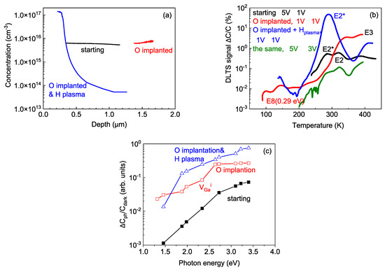
Figure 3.
(a) Evolution of concentration profiles in the β-Ga2O3 sample irradiated with 1016 cm−2 1 MeV O ions. (b) DLTS spectra measured for the starting sample (black line) and for the sample after O implantation (red line) and after O implantation and H plasma treatment (blue line). The olive line corresponds to DLTS spectra measurements in the undamaged bulk of the O-implanted and H plasma-treated sample probed with an applied bias of 5 V and a forward bias pulse of −3 V. (c) LCV measurements for the samples.
DLTS spectra measured for the sample before O implantation showed the presence of the dominant E2, E2* and E3 centers commonly observed in n-type β-Ga2O3 grown by HVPE on native n+ β-Ga2O3 substrates (Figure 3b). DLTS spectra measurements of the quasi-MIS structure formed by O implantation showed signals due to the same traps with the addition of the E8 traps due to radiation defects [37]. These spectra were taken with reverse bias on the MIS structure of −1 V and a forward bias pulse of +1 V and thus probed the region of the interface between the undamaged β-Ga2O3 matrix and the O-implanted damaged region. After H plasma treatment, the C−V profile presented in Figure 3a displays the near-surface region of high electron concentration of about 0.3 µm with a long tail of low net donor density extending into the implanted region to 1.2 µm (Figure 3a). DLTS spectra taken with the bias of −1 V and the forward bias pulse of 1 V, and which thus probed the surface region, are shown in Figure 3b. These demonstrate complete suppression of the E2 traps due to Fe acceptors, with an enhancement of the E2*, E3 and E8 traps. Overall, these results are in line with those obtained after H plasma treatment of the as-grown β-Ga2O3 samples with the () orientation.
The most likely explanation is that hydrogen enters from the plasma and forms donor complexes with abundant VGai formed by O ions. This results in an increased shallow donor concentration. The C−V profiles suggest that the number of H ions introduced from plasma exposure is sufficient to saturate up to the (VGai−4H) state of ~2 × 1017 cm−3 vacancies to a depth of ~0.3 µm. Thus, the density of H ions overshoots the density of Ga vacancies created by irradiation, and the acceptor states due to VGai-nH complexes, if they are formed, are formed deeper inside the sample. This was indirectly confirmed by C−V profiling with the monochromatic illumination photocapacitance spectra (LCV spectra [36]) displayed in Figure 3c. Before the O irradiation, the main feature of the spectra was due to acceptors with an optical ionization threshold near 1.3 eV. After O implantation, a very prominent center with an optical ionization energy close to 2.3 eV attributed to the VGai acceptors emerged. After H plasma treatment, this center was fully quenched because of the formation of complexes with H ions [30].
The above observations suggested that in order to get into the regime where the formation of acceptor complexes with hydrogen from plasma will prevail, the density of radiation defects should be strongly increased, but in such a way as to form predominantly shallow acceptors [32]. To this end, we further irradiated this sample with a higher O fluence of 4 × 1016 cm−3.
The as-implanted sample showed a low current with a current density of 10−9 A/cm2, the capacitance indicating a full depletion of the top 1.4 µm near the surface and the capacitance–voltage characteristic typical for a quasi-MIS structure, with the O-implanted region standing for the “insulator”.
After H plasma treatment, the capacitance versus voltage characteristic was that of an MIS structure (Figure 4). The spectral dependence of these “MIS” characteristics could be deconvoluted into the “oxide” insulator capacitance and the capacitance of the n-region using the values of capacitance in accumulation and depletion [66]. The “oxide” thickness, dox, in the dark was close to the thickness of the heavily damaged region but slightly lower (1.26 µm). With illumination, the thickness of this “oxide” high-resistivity region was first slightly increased to 1.4 µm with a photon energy of 1.35 eV and then gradually decreased with increasing photon energy (Figure 4b). These changes were due to carrier trapping and detrapping effects. The capacitance in depletion behaved correspondingly, indicating that the effective width of the insulating region was also spectrally dependent because part of the implanted layer adjacent to the Schottky diode became more conducting. The corresponding spectral dependence of photocapacitance in accumulation, Cph (high), is shown in Figure 4c. We observed the spectral shift of the voltage corresponding to transition from accumulation to depletion, which allowed us to estimate the change in the sheet density, Ns, of the charge generated in the high-resistivity region from Ns = C(accumulation) × ΔV/(q × S) [66], where C (accumulation) is the capacitance in accumulation, ΔV is the shift of the C−V curve caused by illumination with photons of the given wavelength, q is the charge of the electron and S is the diode area. We did not see evidence of the formation of a conducting n-type or p-type layer at the surface. This might be due to the fact that the density of Ga vacancies greatly increased compared to the 1016 cm−2 O fluence irradiation and the concentration of hydrogen being only sufficient for producing compensating acceptors of VGa, with hydrogen giving rise to the high resistivity. With the (001) orientation, the hydrogen penetration into the sample was 0.3 µm. The situation could become better if HVPE samples with the () orientation were used, so the possibility of achieving the p-n conversion at the surface by H plasma treatment has yet to be proved. Given the situation with respect to variations in defect density created by implantation and the density of hydrogen available for diffusion and complex formation, the task of finding conditions suitable for the preparation of p-type surface films in that way would require optimization.

Figure 4.
(a) C−V characteristics measured for the sample implanted with 4 × 1016 cm−2 oxygen ions and treated in H plasma, with corresponding LED irradiation wavelengths. (b) The spectral dependence of the effective “oxide” thickness calculated from C−V characteristics in (a); also shown is the dark value. (c) The photocapacitance spectrum of the ΔCph (high). (d) Estimated densities and signs of deep traps in the implanted insulating layer.
3.2. α-Ga2O3
We studied two samples of undoped α-Ga2O3 grown by HVPE in the as-grown state and after H plasma treatment. Figure 5a presents the dark current density dependence on voltage for sample GO1058-2 at 300 K in the dark and under illumination with a wavelength of 277 nm and a dark current density at 402 K, all measured on a Ni Schottky diode. There was no rectification in the Schottky diode because of the high resistance of the sample limiting the current flow. The temperature dependence of the current was strong, and the sample showed a high photocurrent obtained under illumination with 277 nm at an optical output power density of 15 mW/cm2. Figure 5b displays the temperature dependence of the current density measured at 5 V after illumination at room temperature and heating up in the dark to 400 K (magenta line), during subsequent cooling down to 140 K in the dark (black line), and after illumination at 140 K and heating up (blue line). From the temperature dependence during cooling from 400 K in the dark (black line), the Fermi level in the film was pinned near EC−0.6 eV. The peaks of the blue and magenta lines corresponding to carrier emission from deep traps filled with light at lower temperature (thermally stimulated current (TSC) [71]) indicate the presence of centers with ionization energies of 0.3, 0.5 and 0.6 eV. Such centers are often observed in undoped HVPE-grown α-Ga2O3 [59]. The PICTS spectra measurements in Figure 5c point to the existence of 0.3 and 0.6 eV traps, also seen in Figure 5b, and an additional deep trap near EC−1.2 eV often encountered in α-Ga2O3 films. The photocurrent at the 5 V spectrum in Figure 5d shows traps filled with electrons and having optical ionization thresholds of 1.3 eV, 2.3 eV and 3.1 eV. No capacitance could be measured for such an as-grown undoped sample.

Figure 5.
(a-GO1058-2) (a) I−V characteristics of undoped α-Ga2O3 film at room temperature in the dark, at room temperature with 277 nm LED illumination and in the dark at 402 K. (b) TSC spectra of the sample. (c) PICTS spectra. The uppermost curve is for the time window of 150 ms/750 ms; the lowermost curve is for the time window of 2550 ms/12,750 ms. (d) The spectral dependence of the photocurrent density at 5 V for undoped α-Ga2O3 film.
After the hydrogen plasma treatment, the capacitance of the sample was easily measured and the carrier density was high (9 × 1018 cm−3), similar to the capacitance of the heavily Sn-doped α-Ga2O3 film with a net donor density of 8.4 × 1018 cm−3 (Figure 6a). No signal from deep traps could be detected in the H plasma-treated sample, in contrast to the Sn-doped sample, where deep traps near EC−0.3 eV and EC−1.2 eV with concentrations near 6 × 1016 cm−3 and 2 × 1016 cm−3, respectively, could be seen (Figure 6b).
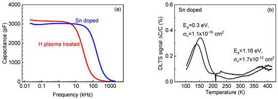
Figure 6.
(a) Comparison of C−f characteristics of the H plasma-treated α-Ga2O3 sample and the α-Ga2O3 sample doped with Sn (both have similar electron concentrations close to 8 × 1018 cm−3 at room temperature. (b) DLTS spectra of the Sn-doped sample (the data shown are for the time windows 0.35 s/3.5 s and 3.5 s/35 s).
For the second undoped α-Ga2O3 sample, GO-1062-2, with properties before hydrogen plasma treatment similar to those of GO-1058-2 hydrogen plasma exposure, there was also a dramatic increase in the capacitance of the Schottky diodes prepared on the treated film (Figure 7a). Cooling the sample to 130 K led to some decrease in capacitance because of freezing out of electrons supplied by the centers introduced by the H plasma. However, illumination with the 277 nm LED increased the capacitance up to the level comparable with room temperature by additional injection of carriers. This capacitance was persistent after the light was switched off and even after the forward bias pulse of 10 s and 1 V was applied. Capacitances at different frequencies measured after illumination remained considerably higher than for the measurement while cooling in the dark up to temperatures close to 400 K, thus suggesting the existence of a barrier for the capture of electrons by centers introduced by the H plasma, similar to the well-known case of DX-like centers [28]. The density of such centers supplying electrons was quite high, close to 1019 cm−3, but slowly decreased with depth (Figure 7c).
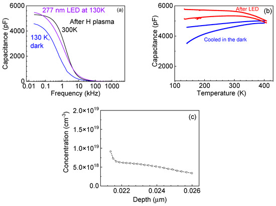
Figure 7.
(Color online) (a) C−f characteristics measured for the H plasma-treated α-Ga2O3 film at room temperature, at 130 K in the dark and at 130 K under 277 nm LED illumination. (b) Capacitance versus temperature measurements at 20 Hz and 200 Hz performed while cooling down in the dark (blue lines) and after illumination at low temperature (red lines). (c) Concentration profile measured in the dark at room temperature.
To sum up the above observations: H plasma treatment of undoped, highly resistive α-Ga2O3 films grown by HVPE on sapphire creates a very high density of centers supplying electrons up to ~1019 cm−3 at room temperature. These centers demonstrate negative-U DX-like behavior implying the presence of a barrier for the capture of electrons photoexcited from the centers at low temperatures. Such centers could be useful in α-Ga2O3-related device technology since standard methods of Si ion implantation and annealing present a problem for α-Ga2O3 because of the low thermal stability of that polymorph. An additional bonus is that the hydrogen plasma produced heavily conducting n-type layers which do not show the high densities of deep traps characteristic of heavily Sn-doped films. It is necessary, however, to check the thermal stability of these H plasma-treatment effects.
3.3. κ-Ga2O3
As discussed in the Introduction, κ-Ga2O3 is of high interest both scientifically and practically because of the high spontaneous electrical polarization field, which greatly exceeds that of GaN or AlN. This has the potential for making possible heterojunction field-effect transistors with very high densities of the two-dimensional electron gas (2DEG) and high saturation currents. The main obstacle to the realization of this potential is the tendency of κ-Ga2O3 films to grow in the form of 120° rotational nanodomains, which strongly handicaps the in-plane current density. One of the ways to partly improve this situation has been proposed by Oshima et al. [64], who used the epitaxial lateral overgrowth (ELOG) approach to radically decrease the density of dislocations and to suppress the formation of rotational nanodomains in the laterally overgrown wings of the ELOG structures deposited on basal-plane sapphire with a thin TiO2 buffer [64]. In earlier work, we used the recipe proposed by Oshima et al. [64] to grow κ-Ga2O3 films with reduced dislocation density and single-domain κ-Ga2O3 structures in the wings and studied the electrical properties, deep trap spectra, and photocurrent and photocapacitance spectra of undoped and Sn-doped ELOG κ-Ga2O3 films. These experiments showed that, even with Sn doping, the donor concentration was quite low, only about 5 × 1012 cm−3.
After H plasma treatment, the capacitance became very high even for undoped samples. Figure 8a shows the data for one such undoped sample at room temperature in the dark and under 277 nm illumination. The concentration obtained from C−V profiling was close to 1019 cm−3 but gradually decreased away from the surface (Figure 8b). The profiles showed sensitivity to light and to heating and cooling under bias, but these features need better understanding. Cooling the sample in the dark led to about 20% decrease in capacitance on the plateau of the C−f dependence. (Figure 8c shows the data for several frequencies on the plateau and for the region of capacitance roll-off with frequency.) After illumination, the capacitance on the plateau became slightly higher than at room temperature and remained persistently high at low temperatures. As the temperature after illumination was increasing, the persistent capacitance stayed virtually unchanged and started to decrease and merged with the dark capacitance in the C versus T dependences above 410 K, slightly increasing with frequency. This behavior is similar to the one observed for the undoped α-Ga2O3 film subjected to plasma treatment (Figure 7b). The activation energies of the carriers that freeze out in the dark as measured in the forward current temperature dependence are also similar, close to 0.1 eV. However, for the ELOG κ-Ga2O3 sample there is a distinction. For frequencies higher than those corresponding to the plateau in the C−f dependence, the temperatures of merging of the persistent and dark C−T curves are lower than for frequencies on the plateau. Moreover, the temperatures of the merging become lower for increasing frequencies. The phenomenon is not fully understood but could be related to the fact that the ELOG κ-Ga2O3 films consist of high-crystalline-quality window regions with a width of 20 µm and of highly defective wing regions with a width of 5 µm. Our measurements performed for Sn-doped films suggest that the wing regions are more resistive and that there is a potential barrier for electrons to penetrate from the wing into the window region. When measuring the capacitance on the C−f plateau, one mostly probes the higher area wing region. However, for frequencies higher than the frequencies corresponding to the plateau, the measured capacitance, C(f), decreases with angular frequency, ω = 2πf, compared to the frequency on the plateau, C0, as C(ω) = C0/[1 + (ωRsC0)2] and is a strong function of the series resistance, Rs [71]. In ELOG κ-Ga2O3, Rs is a function of the potential barrier height between the wing and the window. Illumination decreases this barrier height and increases the capacitance at a high frequency, but the barrier height between the two regions must be lower than the barrier height for the capture of electrons by the centers supplying electrons. This leads to a lower temperature of merging between the dark capacitance and persistent capacitance. However, the detailed picture needs to be established from additional experiments.

Figure 8.
(a) C−f characteristics of the undoped ELOG k-Ga2O3 sample treated in H plasma measured at room temperature in the dark and under 277 nm LED illumination. (b) Concentration profile at room temperature. (c) C−T measurements performed at 20 Hz, 10 kHz, 20 kHz, 30 kHz, 50 kHz, 100 kHz and 200 kHz while cooling in the dark (blue lines) and after illumination at low temperature (red lines). The frequency of 20 kHz (thick lines) corresponds to the start of the capacitance roll-off due to the series resistance effects.
3.4. γ-Ga2O3
The fabrication of these samples is described briefly in the Materials and Methods section. The properties of the samples γ-GO2 and γ-GO3 implanted with Ga ions at 1.7 MeV (fluence: 6 × 1015 cm−2) at room temperature and with 300 keV Si (fluence: 1015 cm−2) and 36 keV Si (fluence: 2 × 1014 cm−2) at 200 °C (sample γ-GaO2, also further annealed to 600 °C) or 400 °C (sample γ-GaO3) have been discussed in some detail previously [69]. Here, we additionally present the results for sample γ-GaO1 implanted only with Ga at room temperature. All samples were prepared by implantation into commercial (010)-oriented β-Ga2O3 EFG-grown bulk crystals compensated with Fe [32]. In the as-implanted state, all samples were highly resistive, with the Fermi level pinned near EC−0.8 eV and the presence of strong potential fluctuations [69]. Structural characterization showed that, after implantation, a thin layer of γ-Ga2O3 with a thickness close to 1 µm was formed. The hydrogen plasma treatment of the Ga-implanted sample γ-GaO1 led to the formation of a conducting layer with a very high capacitance that froze out at 80 K but showed a prominent photocapacitance due to 277 nm illumination that brought the capacitance value to a level close to the one at room temperature. The concentration of the centers responsible for the high capacitance was about 1019 cm−3 at room temperature, based on the results of C−V profiling at room temperature (Figure 9b). This capacitance was persistent and required heating above 400 K to return to the dark value, as can be seen from Figure 9c. The activation energy of the dark current of the forward-biased Schottky diode when cooling in the dark was 95 meV (Figure 9d). This behavior bears a striking resemblance to that shown above for the H plasma-treated α-Ga2O3 and κ-Ga2O3.
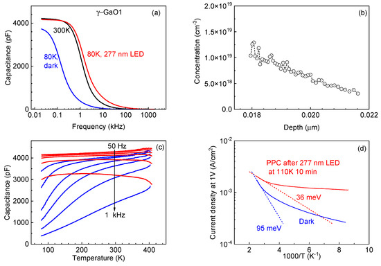
Figure 9.
(a) The 300 K and 80 K dark C−f characteristics and 80 K C−f characteristic measured under 277 nm LED illumination. (b) Concentration profile. (c) C−T characteristics measured while cooling in the dark (blue lines) and while heating up after illumination for different measurement frequencies. (d) TSC spectra for the γ-GaO1 sample implanted with Ga.
The samples γ-GaO2 and γ-GaO3 implanted with Ga and Si showed much lower net donor concentrations of (3–3.5) × 1012 cm−3. Figure 10a shows the corresponding 1/C2 versus V plot for sample γ-GaO2. Both samples were reasonably photosensitive. Figure 10b shows the spectral dependence of the Schottky diode photocurrent at −3 V for samples γ-GaO2 and γ-GaO3. The photosensitivity was 20 times higher for sample γ-GaO3, and both samples showed optical thresholds of 1.3–1.5 eV and 2 eV. The photocapacitance spectra of both samples showed similar optical ionization thresholds. Figure 10c shows the results for sample γ-GaO2.
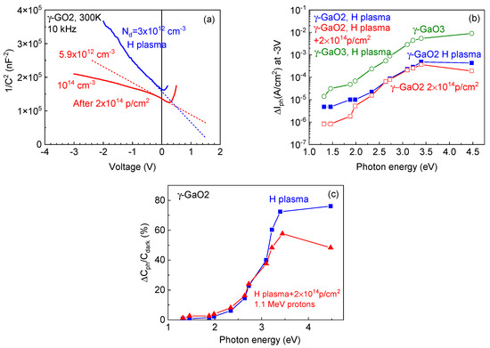
Figure 10.
(a) C−V characteristics of sample γ-GaO2 after H plasma treatment and after additional irradiation with 2 × 10¹⁴ p/cm2 1.1 MeV protons. (b) Spectral dependences of photocurrent at −3 V for samples γ-GaO2 and γ-GaO3 after H plasma treatment. (c) The spectrum for γ-GaO2 after additional proton irradiation with 2 × 10¹⁴ p/cm2 of 1.1 MeV protons; photocapacitance for sample g-GaO2 before and after irradiation with 2 × 10¹⁴ p/cm2 1.1 MeV protons.
As discussed in the Introduction, the results of structural studies for γ-Ga2O3 layers converted from β-Ga2O3 by ion implantation strongly suggest that, structurally, these films are exceptionally radiation tolerant, which is attributed to the peculiar atomic arrangement of γ-Ga2O3 with the structure of cubic defect spinel with a high density of stoichiometric Ga vacancies [25]. There is, however, a question of whether the electrical and optical properties of such films will be of interest for electronic devices. As we saw, the two samples implanted with Ga and Si and treated in H plasma showed a low donor density and measurable photocurrent and could be of interest for trying to fabricate electronic or optoelectronic devices, provided the properties could be improved by optimization.
The other question is whether the radiation tolerance of such structures when assessed by electrical and photoelectrical measurements will indeed be superior to the more established β-Ga2O3. To this end, we compared the electron removal rates in one of the gamma-phase γ-Ga2O3 films, sample γ-GaO2, irradiated with 1.1 MeV protons with a fluence of 2 × 10¹⁴ p/cm2, with that observed in the bulk (001)-oriented β-Ga2O3 sample with a much higher net donor density of 4.3 × 1016 cm−3. The β-Ga2O3 film was fully compensated by such irradiation down to the depth corresponding to the range of 1.1 MeV protons. At the same time, for the sample γ-GaO2 with a much lower electron density of 3 × 1012 cm−3, such proton irradiation only slightly increased the net donor concentration to 5 × 1012 cm−3 (Figure 10a) and only slightly decreased the photosensitivity (Figure 10c).
An interesting question is why the performance is so different for the sample implanted only with Ga and the two samples implanted additionally with high doses of Si. In a simplistic picture, the donors we observe after hydrogen plasma treatment come from: (a) the formation of H complexes with defects, resulting in shallow donors; (b) hydrogen passivation of deep compensating acceptors, thus activating the residual shallow donors; or (c) hydrogen interaction with residual donors, forming deep donor centers. Unfortunately, we know little about the properties of defects and impurities in γ-Ga2O3. General considerations suggest that Fe, which creates a deep compensating acceptor in β-Ga2O3, will behave similarly in γ-Ga2O3 and thus easily form neutral complexes with hydrogen, thus increasing the density of uncompensated residual donors this way but also “wasting” some of the mobile hydrogen that would otherwise form donor complexes with Ga vacancies. If one additionally introduces defects created by Si implantation (whose density is very high in the samples γ-GaO2 and γ-GaO3), the budget of H ions available for increasing the density of electrons could be further moved towards lower values. Some of the products of H interaction with Si-related defects could form deep centers not effective in producing free electrons. In β-Ga2O3, for example, the complexes of Si with hydrogen have been proposed to give rise to deep donor centers near EC−0.6 eV [46]. If this happens in γ-Ga2O3, it would explain the lower efficiency of electron introduction in the samples with combined implantation of Ga and Si. It would seem advisable to repeat the Ga implantation into β-Ga2O3 experiment with samples that do not have high densities of in-grown or implantation related defects that could compromise the effective formation of H-related centers supplying electrons.
4. Conclusions
- In all four Ga2O3 polymorphs treated in dense hydrogen plasma, such treatment has a strong effect on the density of centers supplying electrons and on the density of deep electron and hole traps.
- The similarity of effects in β-, α-, κ- and γ-polymorphs, such as the introduction of a high density of centers supplying electrons, the prominent persistent photoconductivity and photocapacitance, and the similarity of concentrations of such defects introduced by the same kind of hydrogen plasma, limit the range of defects that could be feasible candidates. Such candidates could be hydrogen species, e.g., interstitial hydrogen donors or hydrogen complexes with omnipresent structural defects, likely Ga vacancies, either simple vacancies or split vacancies that are expected to be predominant in all polymorphs.
- The most likely explanation of the observed phenomena seems to be the formation of donor-like complexes of interstitial hydrogen interaction with relaxed or split VGa, with 4Hi and acceptor-like complexes including (2–3) H ions with vacancies.
- The end result depends on the relative number of VGa and Hi determining the relative concentration of VGa−4H complexes (donors) and VGa−2H complexes (acceptors). This is a function of the number and type of defects created by either H plasma or by irradiation of high-energy ions; at least for β-Ga2O3, crystal orientation plays an important role, with the (010) orientation being conducive to deeper H penetration.
- H is effective in “passivating” acceptor centers (Fe, Mg, N and VGa), influencing compensation and recombination.
- H plasma treatment could prove to be useful in the preparation of contact n+ layers in metastable polymorphs not amenable to standard Si implantation and high-temperature annealing commonly requiring annealing temperatures not compatible with the preservation of the metastable polymorph intact.
- All the work desribed here shows that hydrogen has a major influence on the electrical properties of all the polymorphs of Ga2O3 and that attention must be paid to its incorporation during growth and processing steps.
Author Contributions
Conceptualization, A.Y.P. and S.J.P.; methodology, A.Y.P., E.B.Y., V.I.N., A.I.P., A.V.M., A.A., A.A.V. and I.V.S.; software, A.A.V., I.V.S. and S.J.P.; validation, A.Y.P., E.B.Y., V.I.N., A.K. and I.-H.L.; formal analysis, A.Y.P., A.K. and I.-H.L.; investigation, A.Y.P., E.B.Y., V.I.N., A.I.P., A.K., A.A., A.A.V., A.I.K. and I.V.S.; resources, A.Y.P., V.I.N., A.I.P., A.V.M., A.K., A.A., I.-H.L. and S.J.P.; data curation, A.Y.P., A.A., A.A.V., A.I.K. and I.V.S.; writing—original draft preparation, A.Y.P., E.B.Y. and S.J.P.; writing—review and editing, I.-H.L., A.A.V., A.I.K. and S.J.P.; visualization, A.Y.P., A.A.V. and A.I.K.; supervision, A.Y.P. and S.J.P.; project administration, A.Y.P., A.K. and S.J.P.; funding acquisition, A.Y.P., E.B.Y., A.K. and S.J.P. All authors have read and agreed to the published version of the manuscript.
Funding
The research at NUST MISIS was funded by Ministry of Science and Higher Education of the Russian Federation grant number 075-15-2022-1113. The research at the University of Oslo was funded by the Research Council of Norway project numbers 337627 and 322382 and by the Norwegian Directorate for Higher Education and Skills project number UTF-2021/10210. The research at the University of Florida was funded by the Department of Defense, the Defense Threat Reduction Agency, grant number HDTRA1–20–2–0002.
Data Availability Statement
The data that support the findings of this study are available within the article.
Acknowledgments
The work at NUST MISIS was supported in part by a grant from the Ministry of Science and Higher Education of the Russian Federation (agreement number 075-15-2022-1113). The work at the University of Oslo was enabled by the M-ERA.NET funds administrated by the Research Council of Norway via project number 337627, as well as the INTPART program at the Research Council of Norway via project number 322382 and the UTFORSK program funded by the Norwegian Directorate for Higher Education and Skills via project UTF-2021/10210. The work at the University of Florida was performed as part of the Interaction of Ionizing Radiation with Matter University Research Alliance (IIRM-URA) sponsored by the Department of Defense, the Defense Threat Reduction Agency, under award HDTRA1–20–2–0002.
Conflicts of Interest
The authors declare no conflict of interest.
References
- Pearton, S.J.; Ren, F.; Tadjer, M.; Kim, J. Perspective: Ga2O3 for Ultra-High Power Rectifiers and MOSFETS. J. Appl. Physics. Am. Inst. Phys. Inc. 2018, 124, 220901. Available online: https://pubs.aip.org/aip/jap/article/124/22/220901/155633/Perspective-Ga2O3-for-ultra-high-power-rectifiers (accessed on 1 September 2023). [CrossRef]
- Higashiwaki, M.; Fujita, S. Springer Series in Materials Science 293 Gallium Oxide Materials Properties, Crystal Growth, and Devices; Springer: Berlin/Heidelberg, Germany, 2020; Available online: https://link.springer.com/book/10.1007/978-3-030-37153-1 (accessed on 1 September 2023).
- Xu, J.; Zheng, W.; Huang, F. Gallium Oxide Solar-Blind Ultraviolet Photodetectors: A Review. J. Mater. Chem. C R. Soc. Chem. 2019, 7, 8753–8770. Available online: https://pubs.rsc.org/en/content/articlelanding/2019/tc/c9tc02055a (accessed on 1 September 2023). [CrossRef]
- Speck, J.S.; Farzana, E. Ultrawide Bandgap β-Ga2O3 Semiconductor Theory and Applications; AIP Publishing LLC: New York, NY, USA, 2023. [Google Scholar] [CrossRef]
- Kaneko, K.; Fujita, S.; Hitora, T. A power device material of corundum-structured α-Ga2O3 fabricated by MIST EPITAXY® technique. Jpn. J. Appl. Phys. Jpn. Soc. Appl. Phys. 2018, 57, 02CB18. [Google Scholar] [CrossRef]
- Ahmadi, E.; Oshima, Y. Materials issues and devices of α- and β-Ga2O3. J. Appl. Phys. Am. Inst. Phys. Inc. 2019, 126, 160901. [Google Scholar] [CrossRef]
- Bae, J.; Park, J.-H.; Jeon, D.-W.; Kim, J. Self-Powered Solar-Blind α-Ga2O3 Thin-Film UV-C Photodiode Grown by Halide Vapor-Phase Epitaxy. APL Mater. Am. Inst. Phys. Inc. 2021, 9, 101108. Available online: https://pubs.aip.org/aip/apm/article/9/10/101108/123072/Self-powered-solar-blind-Ga2O3-thin-film-UV-C (accessed on 1 September 2023). [CrossRef]
- Kaneko, K.; Masuda, Y.; Kan, S.; Takahashi, I.; Kato, Y.; Shinohe, T.; Fujita, S. Ultra-Wide Bandgap Corundum-Structured p-Type α-(Ir,Ga)2O3 Alloys for α-Ga2O3 Electronics. Appl. Phys. Lett. Am. Inst. Phys. Inc. 2021, 118, 102104. Available online: https://pubs.aip.org/aip/apl/article-abstract/118/10/102104/1058736/Ultra-wide-bandgap-corundum-structured-p-type-Ir?redirectedFrom=fulltext (accessed on 1 September 2023). [CrossRef]
- Peelaers, H.; Lyons, J.L.; Varley, J.B.; Van de Walle, C.G. Deep acceptors and their diffusion in Ga2O3. APL Mater. Am. Inst. Phys. Inc. 2019, 7, 022519. [Google Scholar] [CrossRef]
- Oshima, Y.; Ando, H.; Shinohe, T. Reduction of Dislocation Density in α-Ga2O3 Epilayers via Rapid Growth at Low Temperatures by Halide Vapor Phase Epitaxy. Appl. Phys. Express 2023, 16, 065501. Available online: https://iopscience.iop.org/article/10.35848/1882-0786/acddca (accessed on 1 September 2023). [CrossRef]
- McCandless, J.P.; Chang, C.S.; Nomoto, K.; Casamento, J.; Protasenko, V.; Vogt, P.; Rowe, D.; Gann, K.; Ho, S.T.; Li, W.; et al. Thermal Stability of Epitaxial α-Ga2O3 and (Al,Ga)2O3layers on m-Plane Sapphire. Appl. Phys. Lett. Am. Inst. Phys. Inc. 2021, 119, 062102. Available online: https://pubs.aip.org/aip/apl/article/119/6/062102/41883/Thermal-stability-of-epitaxial-Ga2O3-and-Al-Ga-2O3 (accessed on 1 September 2023). [CrossRef]
- Mezzadri, F.; Calestani, G.; Boschi, F.; Delmonte, D.; Bosi, M.; Fornari, R. Crystal Structure and Ferroelectric Properties of ε-Ga2O3 Films Grown on (0001)-Sapphire. Inorg. Chem. 2016, 55, 12079–12084. Available online: https://pubs.acs.org/doi/10.1021/acs.inorgchem.6b02244 (accessed on 1 September 2023). [CrossRef]
- Parisini, A.; Bosio, A.; Montedoro, V.; Gorreri, A.; Lamperti, A.; Bosi, M.; Garulli, G.; Vantaggio, S.; Fornari, R. Si and Sn Doping of ε-Ga2O3 Layers. APL Mater. 2019, 7, 031114. Available online: https://pubs.aip.org/aip/apm/article/7/3/031114/1024354/Si-and-Sn-doping-of-Ga2O3-layers (accessed on 1 September 2023). [CrossRef]
- Von Wenckstern, H. Group-III Sesquioxides: Growth, Physical Properties and Devices. Adv. Electron. Mater. 2017, 3, 1600350. Available online: https://onlinelibrary.wiley.com/doi/abs/10.1002/aelm.201600350 (accessed on 1 September 2023). [CrossRef]
- Wang, J.; Guo, H.; Zhu, C.-Z.; Cai, Q.; Yang, G.-F.; Xue, J.-J.; Chen, D.-J.; Tong, Y.; Liu, B.; Lu, H.; et al. ε-Ga2O3: A Promising Candidate for High-Electron-Mobility Transistors. IEEE Electron. Device Lett. 2020, 41, 1052–1055. Available online: https://ieeexplore.ieee.org/document/9095303 (accessed on 1 September 2023). [CrossRef]
- Cho, S.B.; Mishra, R. Epitaxial Engineering of Polar ε-Ga2O3 for Tunable Two-Dimensional Electron Gas at the Heterointerface. Appl. Phys. Lett. 2018, 112, 162101. Available online: https://pubs.aip.org/aip/apl/article/112/16/162101/35526/Epitaxial-engineering-of-polar-Ga2O3-for-tunable (accessed on 1 September 2023). [CrossRef]
- Polyakov, A.Y.; Nikolaev, V.I.; Pechnikov, A.I.; Yakimov, E.B.; Karpov, S.Y.; Stepanov, S.I.; Shchemerov, I.V.; Vasilev, A.A.; Chernykh, A.V.; Kuznetsov, A.; et al. Two-Dimensional Hole Gas Formation at the κ-Ga2O3/AlN Heterojunction Interface. J. Alloys Compd. 2023, 936, 168315. Available online: https://www.sciencedirect.com/science/article/abs/pii/S0925838822047065 (accessed on 1 September 2023). [CrossRef]
- Chen, Z.; Lu, X.; Tu, Y.; Chen, W.; Zhang, Z.; Cheng, S.; Chen, S.; Luo, H.; He, Z.; Pei, Y.; et al. ε-Ga2O3: An Emerging Wide Bandgap Piezoelectric Semiconductor for Application in Radio Frequency Resonators. Adv. Sci. 2022, 9, 2203927. Available online: https://onlinelibrary.wiley.com/doi/full/10.1002/advs.202203927 (accessed on 1 September 2023). [CrossRef] [PubMed]
- Mu, S.; Van de Walle, C.G. Phase Stability of (AlxGa1−x)2O3 Polymorphs: A First-Principles Study. Phys. Rev. Mater. 2022, 6, 104601. Available online: https://journals.aps.org/prmaterials/abstract/10.1103/PhysRevMaterials.6.104601 (accessed on 1 September 2023). [CrossRef]
- Cora, I.; Fogarassy, Z.; Fornari, R.; Bosi, M.; Recnik, A.; Pécz, B. In Situ TEM Study of κ→β and κ→γ Phase Transformations in Ga2O3. Acta Mater. 2020, 183, 216–227. Available online: https://www.sciencedirect.com/science/article/abs/pii/S1359645419307505 (accessed on 1 September 2023). [CrossRef]
- García-Fernández, J.; Kjeldby, S.B.; Nguyen, P.D.; Karlsen, O.B.; Vines, L.; Prytz, Ø. Formation of γ-Ga2O3 by ion Implantation: Polymorphic Phase Transformation of β-Ga2O3. Appl. Phys. Lett. 2022, 121, 191601. Available online: https://pubs.aip.org/aip/apl/article-abstract/121/19/191601/2834492/Formation-of-Ga2O3-by-ion-implantation-Polymorphic?redirectedFrom=fulltext (accessed on 1 September 2023). [CrossRef]
- Azarov, A.; Bazioti, C.; Venkatachalapathy, V.; Vajeeston, P.; Monakhov, E.; Kuznetsov, A. Disorder-Induced Ordering in Gallium Oxide Polymorphs. Phys. Rev. Lett. 2022, 128, 015704. Available online: https://journals.aps.org/prl/abstract/10.1103/PhysRevLett.128.015704 (accessed on 1 September 2023). [CrossRef]
- Anber, E.A.; Foley, D.; Lang, A.C.; Nathaniel, J.; Hart, J.L.; Tadjer, M.J.; Hobart, K.D.; Pearton, S.; Taheri, M.L. Structural Transition and Recovery of Ge Implanted β-Ga2O3. Appl. Phys. Lett. 2020, 117, 152101. Available online: https://pubs.aip.org/aip/apl/article/117/15/152101/1061356/Structural-transition-and-recovery-of-Ge-implanted (accessed on 1 September 2023). [CrossRef]
- Huang, H.-L.; Chae, C.; Johnson, J.M.; Senckowski, A.; Sharma, S.; Singisetti, U.; Wong, M.H.; Hwang, J. Atomic Scale Defect Formation and Phase Transformation in Si Implanted β-Ga2O3. APL Mater. 2023, 11, 061113. Available online: https://pubs.aip.org/aip/apm/article/11/6/061113/2894427/Atomic-scale-defect-formation-and-phase (accessed on 1 September 2023). [CrossRef]
- Azarov, A.; García Fernández, J.; Zhao, J.; Djurabekova, F.; He, H.; He, R.; Prytz, Ø.; Vines, L.; Bektas, U.; Chekhonin, P.; et al. Universal Radiation Tolerant Semiconductor. Nat. Commun. 2023, 14, 4855. Available online: https://www.nature.com/articles/s41467-023-40588-0 (accessed on 1 September 2023). [CrossRef]
- Varley, J.B.; Weber, J.R.; Janotti, A.; van de Walle, C.G. Oxygen Vacancies and Donor Impurities in β-Ga2O3. Appl. Phys. Lett. 2010, 97, 142106. Available online: https://pubs.aip.org/aip/apl/article-abstract/97/14/142106/1023190/Oxygen-vacancies-and-donor-impurities-in-Ga2O3?redirectedFrom=fulltext (accessed on 1 September 2023). [CrossRef]
- Varley, J.B.; Peelaers, H.; Janotti, A.; van de Walle, C.G. Hydrogenated Cation Vacancies in Semiconducting Oxides. J. Phys. Condens. Matter 2011, 23, 334212. Available online: https://iopscience.iop.org/article/10.1088/0953-8984/23/33/334212/meta (accessed on 1 September 2023). [CrossRef] [PubMed]
- Langørgen, A.; Zimmermann, C.; Kalmann Frodason, Y.; Førdestrøm Verhoeven, E.; Weiser, P.M.; Karsthof, R.M.; Varley, J.B.; Vines, L. Influence of Heat Treatments in H2 and Ar on the E1 center in β-Ga2O3. J. Appl. Phys. 2022, 131, 115702. Available online: https://pubs.aip.org/aip/jap/article/131/11/115702/2836786/Influence-of-heat-treatments-in-H2-and-Ar-on-the (accessed on 1 September 2023). [CrossRef]
- Swallow, J.E.N.; Varley, J.B.; Jones, L.A.H.; Gibbon, J.T.; Piper, L.F.J.; Dhanak, V.R.; Veal, T.D. Transition from Electron Accumulation to Depletion at β-Ga2O3 Surfaces: The Role of Hydrogen and the Charge Neutrality Level. APL Mater. 2019, 7, 022528. Available online: https://pubs.aip.org/aip/apm/article/7/2/022528/1064149/Transition-from-electron-accumulation-to-depletion (accessed on 1 September 2023). [CrossRef]
- Ingebrigtsen, M.E.; Kuznetsov, A.Y.; Svensson, B.G.; Alfieri, G.; Mihaila, A.; Badstubner, U.; Perron, A.; Vines, L.; Varley, J.B. Impact of Proton Irradiation on Conductivity and Deep Level Defects in β-Ga2O3. APL Mater. 2019, 7, 022510. Available online: https://pubs.aip.org/aip/apm/article/7/2/022510/1064089/Impact-of-proton-irradiation-on-conductivity-and (accessed on 1 September 2023). [CrossRef]
- Deák, P.; Ho, Q.D.; Seemann, F.; Aradi, B.; Lorke, M.; Frauenheim, T. Choosing the Correct Hybrid for Defect Calculations: A case Study on Intrinsic Carrier Trapping in β−Ga2O3. Phys. Rev. B 2017, 95, 075208. Available online: https://journals.aps.org/prb/abstract/10.1103/PhysRevB.95.075208 (accessed on 1 September 2023). [CrossRef]
- Islam, M.M.; Liedke, M.O.; Winarski, D.; Butterling, M.; Wagner, A.; Hosemann, P.; Wang, Y.; Uberuaga, B.; Selim, F.A. Chemical Manipulation of Hydrogen Induced High p-Type and N-Type Conductivity in Ga2O3. Sci. Rep. 2020, 10, 6134. Available online: https://www.nature.com/articles/s41598-020-62948-2 (accessed on 1 September 2023). [CrossRef]
- Karjalainen, A.; Prozheeva, V.; Simula, K.; Makkonen, I.; Callewaert, V.; Varley, J.B.; Tuomisto, F. Split Ga Vacancies and the Unusually Strong Anisotropy of Positron Annihilation Spectra in β−Ga2O3. Phys. Rev. B 2020, 102, 195207. Available online: https://journals.aps.org/prb/abstract/10.1103/PhysRevB.102.195207 (accessed on 1 September 2023). [CrossRef]
- Portoff, A.; Venzie, A.; Stavola, M.; Fowler, W.B.; Glaser, E.; Pearton, S.J. Classes of O–D Centers in Unintentionally and Fe-doped β-Ga2O3 Annealed in a D2 Ambient. J. Appl. Phys. 2023, 134, 045701. Available online: https://pubs.aip.org/aip/jap/article-abstract/134/4/045701/2904193/Classes-of-O-D-centers-in-unintentionally-and-Fe?redirectedFrom=fulltext (accessed on 1 September 2023). [CrossRef]
- Huang, H.-L.; Chae, C.; Hwang, J. Perspective on Atomic Scale Investigation of Point and Extended Defects in Gallium Oxide. J. Appl. Phys. 2022, 131, 190901. Available online: https://pubs.aip.org/aip/jap/article/131/19/190901/2836854/Perspective-on-atomic-scale-investigation-of-point (accessed on 1 September 2023). [CrossRef]
- Zhang, Z.; Farzana, E.; Arehart, A.R.; Ringel, S.A. Deep Level Defects Throughout the Bandgap of (010) β-Ga2O3 Detected by Optically and Thermally Stimulated Defect Spectroscopy. Appl. Phys. Lett. 2016, 108, 052105. Available online: https://pubs.aip.org/aip/apl/article/108/5/052105/1022811/Deep-level-defects-throughout-the-bandgap-of-010 (accessed on 1 September 2023). [CrossRef]
- Polyakov, A.Y.; Nikolaev, V.I.; Yakimov, E.B.; Ren, F.; Pearton, S.J.; Kim, J. Deep Level Defect States in β-, α-, and ε-Ga2O3 Crystals and Films: Impact on Device Performance. J. Vac. Sci. Technol. A 2022, 40, 020804. Available online: https://pubs.aip.org/avs/jva/article/40/2/020804/2843491/Deep-level-defect-states-in-and-Ga2O3-crystals-and (accessed on 1 September 2023). [CrossRef]
- Karjalainen, A.; Weiser, P.M.; Makkonen, I.; Reinertsen, V.M.; Vines, L.; Tuomisto, F. Interplay of Vacancies, Hydrogen, and Electrical Compensation in Irradiated and Annealed n-β-Ga2O3. J. Appl. Phys. 2021, 129, 165702. Available online: https://pubs.aip.org/aip/jap/article-abstract/129/16/165702/157758/Interplay-of-vacancies-hydrogen-and-electrical?redirectedFrom=fulltext (accessed on 1 September 2023). [CrossRef]
- Sharma, R.; Patrick, E.; Law, M.E.; Ahn, S.; Ren, F.; Pearton, S.J.; Kuramata, A. Extraction of Migration Energies and Role of Implant Damage on Thermal Stability of Deuterium in Ga2O3. ECS J. Solid. State Sci. Technol. 2017, 6, P794–P797. Available online: https://iopscience.iop.org/article/10.1149/2.0201712jss (accessed on 1 September 2023). [CrossRef]
- Fowler, W.B.; Stavola, M.; Qin, Y.; Weiser, P. Trapping of Multiple H Atoms at the Ga(1) Vacancy in β-Ga2O3. Appl. Phys. Lett. 2020, 117, 142101. Available online: https://pubs.aip.org/aip/apl/article/117/14/142101/1056584/Trapping-of-multiple-H-atoms-at-the-Ga-1-vacancy (accessed on 1 September 2023). [CrossRef]
- Portoff, A.; Venzie, A.; Qin, Y.; Stavola, M.; Fowler, W.B.; Pearton, S.J. Vibrational Properties of Oxygen-Hydrogen Centers in H+- and D+-Implanted Ga2O3. ECS J. Solid. State Sci. Technol. 2020, 9, 125006. Available online: https://iopscience.iop.org/article/10.1149/2162-8777/abd458 (accessed on 1 September 2023). [CrossRef]
- Venzie, A.; Portoff, A.; Perez Valenzuela, E.C.; Stavola, M.; Fowler, W.B.; Pearton, S.J.; Glaser, E.R. Impurity-Hydrogen Complexes in β-Ga2O3: Hydrogenation of Shallow Donors vs Deep Acceptors. J. Appl. Phys. 2022, 131, 035706. Available online: https://pubs.aip.org/aip/jap/article/131/3/035706/2836457/Impurity-hydrogen-complexes-in-Ga2O3-Hydrogenation (accessed on 1 September 2023). [CrossRef]
- Weiser, P.; Stavola, M.; Fowler, W.B.; Qin, Y.; Pearton, S. Structure and Vibrational Properties of the Dominant O-H Center in β-Ga2O3. Appl. Phys. Lett. 2018, 112, 232104. Available online: https://pubs.aip.org/aip/apl/article/112/23/232104/279988/Structure-and-vibrational-properties-of-the (accessed on 1 September 2023). [CrossRef]
- Nickel, N.H. Hydrogen Incorporation in Semiconductors. In Physica Status Solidi (b); John Wiley & Sons: Hoboken, NJ, USA, 2023; Available online: https://onlinelibrary.wiley.com/doi/pdf/10.1002/pssb.202300309 (accessed on 1 September 2023).
- Tuomisto, F. Ga Vacancies in β-Ga2O3: Split or not? Jpn. J. Appl. Phys. 2023, 62, SF0802. Available online: https://iopscience.iop.org/article/10.35848/1347-4065/acc7b1/meta (accessed on 1 September 2023). [CrossRef]
- Polyakov, A.Y.; Lee, I.-H.; Smirnov, N.B.; Shchemerov, I.V.; Vasilev, A.A.; Chernykh, A.V.; Pearton, S.J. Electric Field Dependence of Major Electron Trap Emission in Bulk β-Ga2O3: Poole–Frenkel Effect Versus Phonon-Assisted Tunneling. J. Phys. D Appl. Phys. 2020, 53, 304001. Available online: https://iopscience.iop.org/article/10.1088/1361-6463/ab87c1 (accessed on 1 September 2023). [CrossRef]
- Polyakov, A.Y.; Lee, I.-H.; Miakonkikh, A.; Chernykh, A.V.; Shchemerov, I.V.; Kochkova, A.I.; Vasilev, A.A.; Pearton, S.J. Anisotropy of Hydrogen Plasma Effects in Bulk n-type β-Ga2O3. J. Appl. Phys. 2020, 127, 175702. Available online: https://pubs.aip.org/aip/jap/article/127/17/175702/157157/Anisotropy-of-hydrogen-plasma-effects-in-bulk-n (accessed on 1 September 2023). [CrossRef]
- Polyakov, A.Y.; Lee, I.-H.; Smirnov, N.B.; Yakimov, E.B.; Shchemerov, I.V.; Chernykh, A.V.; Kochkova, A.I.; Vasilev, A.A.; Shiko, A.S.; Carey IV, P.H.; et al. Effects of Hydrogen Plasma Treatment Condition on Electrical Properties of β-Ga2O3. ECS J. Solid. State Sci. Technol. 2019, 8, P661–P666. Available online: https://iopscience.iop.org/article/10.1149/2.0041911jss (accessed on 1 September 2023). [CrossRef]
- Ahn, S.; Ren, F.; Patrick, E.; Law, M.E.; Pearton, S.J. Thermal Stability of Implanted or Plasma Exposed Deuterium in Single Crystal Ga2O3. ECS J. Solid. State Sci. Technol. 2017, 6, Q3026–Q3029. Available online: https://iopscience.iop.org/article/10.1149/2.0051702jss (accessed on 1 September 2023). [CrossRef]
- Reinertsen, V.M.; Weiser, P.M.; Frodason, Y.K.; Bathen, M.E.; Vines, L.; Johansen, K.M. Anisotropic and Trap-Limited Diffusion of Hydrogen/Deuterium in Monoclinic Gallium Oxide Single Crystals. Appl. Phys. Lett. 2020, 117, 232106. Available online: https://pubs.aip.org/aip/apl/article-abstract/117/23/232106/1022373/Anisotropic-and-trap-limited-diffusion-of-hydrogen?redirectedFrom=fulltext (accessed on 1 September 2023). [CrossRef]
- Pearton, S.J.; Corbett, J.W.; Stavola, M. Hydrogen in Crystalline Semiconductors; Springer: Berlin/Heidelberg, Germany, 1992; Volume 16, Available online: https://link.springer.com/article/10.1007/BF00615975 (accessed on 1 September 2023).
- Zimmermann, C.; Verhoeven, E.F.; Frodason, Y.K.; Weiser, P.M.; Varley, J.B.; Vines, L. Formation and Control of the E2∗ Center in Implanted β-Ga2O3 by Reverse-Bias and Zero-Bias Annealing. J. Phys. D Appl. Phys. 2020, 53, 464001. Available online: https://iopscience.iop.org/article/10.1088/1361-6463/aba64d (accessed on 1 September 2023). [CrossRef]
- Frodason, Y.K.; Zimmermann, C.; Verhoeven, E.F.; Weiser, P.M.; Vines, L.; Varley, J.V. Multistability of Isolated and Hydrogenated Ga–O Divacancies in β-Ga2O3. Phys. Rev. Mater. 2021, 5, 025402. Available online: https://journals.aps.org/prmaterials/abstract/10.1103/PhysRevMaterials.5.025402 (accessed on 1 September 2023). [CrossRef]
- Polyakov, A.Y.; Smirnov, N.B.; Shchemerov, I.V.; Pearton, S.J.; Ren, F.; Chernykh, A.V.; Lagov, P.B.; Kulevoy, T.V. Hole traps and persistent photocapacitance in proton irradiated β-Ga2O3 films doped with Si. APL Mater. 2018, 6, 096102. [Google Scholar] [CrossRef]
- Polyakov, A.Y.; Lee, I.-H.; Smirnov, N.B.; Yakimov, E.B.; Shchemerov, I.V.; Chernykh, A.V.; Kochkova, A.I.; Vasilev, A.A.; Ren, F.; Carey, P.H.; et al. Hydrogen Plasma Treatment of β-Ga2O3: Changes in Electrical Properties and Deep Trap Spectra. Appl. Phys. Lett. 2019, 115, 032101. Available online: https://pubs.aip.org/aip/apl/article/115/3/032101/37981/Hydrogen-plasma-treatment-of-Ga2O3-Changes-in (accessed on 1 September 2023). [CrossRef]
- Polyakov, A.Y.; Nikolaev, V.I.; Pechnikov, A.I.; Lagov, P.B.; Shchemerov, I.V.; Vasilev, A.A.; Chernykh, A.V.; Kochkova, A.I.; Guzilova, L.; Pavlov, Y.S.; et al. Carrier Removal Rates in 1.1 MeV Proton Irradiated α-Ga2O3 (Sn). J. Phys. D Appl. Phys. 2023, 56, 305103. Available online: https://iopscience.iop.org/article/10.1088/1361-6463/acd06b (accessed on 1 September 2023). [CrossRef]
- Polyakov, A.Y.; Nikolaev, V.I.; Stepanov, S.I.; Pechnikov, A.I.; Yakimov, E.B.; Smirnov, N.B.; Shchemerov, I.V.; Vasilev, A.A.; Kochkova, A.I.; Chernykh, A.V.; et al. Editors’ Choice—Electrical Properties and Deep Traps in α-Ga2O3:Sn Films Grown on Sapphire by Halide Vapor Phase Epitaxy. ECS J. Solid. State Sci. Technol. 2020, 9, 045003. Available online: https://iopscience.iop.org/article/10.1149/2162-8777/ab89bb (accessed on 1 September 2023). [CrossRef]
- Kobayashi, T.; Gake, T.; Kumagai, Y.; Oba, F.; Matsushita, Y. Energetics and Electronic Structure of Native Point Defects in α-Ga2O3. Appl. Phys. Express 2019, 12, 091001. Available online: https://iopscience.iop.org/article/10.7567/1882-0786/ab3763 (accessed on 1 September 2023). [CrossRef]
- Polyakov, A.; Nikolaev, V.; Stepanov, S.; Almaev, A.; Pechnikov, A.; Yakimov, E.; Kushnarev, B.O.; Shchemerov, I.; Scheglov, M.; Chernykh, A.; et al. Electrical Properties of α-Ga2O3 Films Grown by Halide Vapor Phase Epitaxy on Sapphire with α-Cr2O3 Buffers. J. Appl. Phys. 2022, 131, 215701. Available online: https://pubs.aip.org/aip/jap/article/131/21/215701/2837032/Electrical-properties-of-Ga2O3-films-grown-by (accessed on 1 September 2023). [CrossRef]
- Venzie, A.; Portoff, A.; Stavola, M.; Fowler, W.B.; Kim, J.; Jeon, D.-W.; Park, J.-H.; Pearton, S.J. H Trapping at the Metastable Cation Vacancy in α-Ga2O3 and α-Al2O3. Appl. Phys. Lett. 2022, 120, 192101. Available online: https://pubs.aip.org/aip/apl/article/120/19/192101/2833581/H-trapping-at-the-metastable-cation-vacancy-in (accessed on 1 September 2023). [CrossRef]
- Azarov, A.; Park, J.-H.; Jeon, D.-W.; Kuznetsov, A. High mobility of intrinsic defects in α-Ga2O3. Appl. Phys. Lett. 2023, 122, 182104. [Google Scholar] [CrossRef]
- Kneiß, M.; Splith, D.; Schlupp, P.; Hassa, A.; von Wenckstern, H.; Lorenz, M.; Grundmann, M. Realization of Highly Rectifying Schottky Barrier Diodes and pn Heterojunctions on κ-Ga2O3 by Overcoming the Conductivity Anisotropy. J. Appl. Phys. 2021, 130, 084502. Available online: https://pubs.aip.org/aip/jap/article/130/8/084502/568036/Realization-of-highly-rectifying-Schottky-barrier (accessed on 1 September 2023). [CrossRef]
- Polyakov, A.Y.; Nikolaev, V.I.; Pechnikov, A.I.; Stepanov, S.I.; Yakimov, E.B.; Scheglov, M.P.; Shchemerov, I.V.; Vasilev, A.A.; Kochkova, A.I.; Chernykh, A.V.; et al. Structural and Electrical Properties of Thick κ-Ga2O3 Grown on GaN/Sapphire Templates. APL Mater. 2022, 10, 061102. Available online: https://pubs.aip.org/aip/apm/article/10/6/061102/2835021/Structural-and-electrical-properties-of-thick (accessed on 1 September 2023). [CrossRef]
- Oshima, Y.; Kawara, K.; Oshima, T.; Shinohe, T. In-Plane Orientation Control of (001) κ-Ga2O3 by Epitaxial Lateral Overgrowth through a Geometrical Natural Selection Mechanism. Jpn. J. Appl. Phys. 2020, 59, 115501. Available online: https://iopscience.iop.org/article/10.35848/1347-4065/abbc57 (accessed on 1 September 2023). [CrossRef]
- Beall Fowler, W. Private communication; Academic Press: New York, NY, USA, 2023. [Google Scholar]
- Li, J.V.; Ferrari, G. Capacitance Spectroscopy of Semiconductors; Jenny Stanford Publishing: Dubai, United Arab Emirates, 2018. [Google Scholar]
- Polyakov, A.Y.; Vasilev, A.A.; Shchemerov, I.V.; Chernykh, A.V.; IShetinin, I.V.; Zhevnerov, E.V.; Kochkova, A.I.; Lagov, P.B.; Miakonkikh, A.V.; Pavlov, Y.S.; et al. Conducting Surface Layers Formed by Hydrogenation of O-Implanted β-Ga2O3. J. Alloys Compd. 2023, 945, 169258. Available online: https://papers.ssrn.com/sol3/papers.cfm?abstract_id=4336746 (accessed on 1 September 2023). [CrossRef]
- Nikolaev, V.I.; Polyakov, A.Y.; Stepanov, S.I.; Pechnikov, A.I.; Yakimov, E.B.; Chernykh, A.V.; Vasilev, A.A.; Shchemerov, I.V.; Kochkova, A.I.; Guzilova, L.; et al. Electrical and Structural Properties of Two-Inch Diameter (0001) α-Ga2O3 Films Doped with Sn and Grown by Halide Epitaxy. ECS J. Solid State Sci. Technol. 2022, 11, 115002. Available online: https://iopscience.iop.org/article/10.1149/2162-8777/ac9edb (accessed on 1 September 2023). [CrossRef]
- Polyakov, A.Y.; Kochkova, A.I.; Azarov, A.; Venkatachalapathy, V.; Miakonkikh, A.V.; Vasilev, A.A.; Chernykh, A.V.; Shchemerov, I.V.; Romanov, A.A.; Kuznetsov, A.; et al. Tuning Electrical Properties in Ga2O3 Polymorphs Induced with Ion Beams. J. Appl. Phys. 2023, 133, 095701. Available online: https://pubs.aip.org/aip/jap/article-abstract/133/9/095701/2879260/Tuning-electrical-properties-in-Ga2O3-polymorphs?redirectedFrom=fulltext (accessed on 1 September 2023). [CrossRef]
- Tapiero, M.; Benjelloun, N.; Zielinger, J.P.; El Hamd, S.; Noguet, C. Photoinduced Current Transient Spectroscopy in High-resistivity Bulk Materials: Instrumentation and Methodology. J. Appl. Phys. 1988, 64, 4006–4012. Available online: https://pubs.aip.org/aip/jap/article-abstract/64/8/4006/15474/Photoinduced-current-transient-spectroscopy-in?redirectedFrom=fulltext (accessed on 1 September 2023). [CrossRef]
- Schroder, D.K. Semiconductor Material and Device Characterization; John Wiley & Sons: Hoboken, NJ, USA, 2005. [Google Scholar]
- Polyakov, A.Y.; Shmidt, N.M.; Smirnov, N.B.; Shchemerov, I.V.; Shabunina, E.I.; Tal’nishnih, N.A.; Lee, I.-H.; Alexanyan, L.A.; Tarelkin, S.A.; Pearton, S.J. Deep Trap Analysis in Green Light Emitting Diodes: Problems and Solutions. J. Appl. Phys. 2019, 125, 215701. Available online: https://pubs.aip.org/aip/jap/article-abstract/125/21/215701/964545/Deep-trap-analysis-in-green-light-emitting-diodes?redirectedFrom=fulltext (accessed on 1 September 2023). [CrossRef]
- Yakimov, E.B. Study of Wide-Gap Semiconductors Using Electron-Beam Induced Current Method. Crystallogr. Rep. 2021, 66, 581–593. [Google Scholar] [CrossRef]
- Donolato, C. A Reciprocity Theorem for Charge Collection. Appl. Phys. Lett. 1985, 46, 270–272. Available online: https://pubs.aip.org/aip/apl/article-abstract/46/3/270/50054/A-reciprocity-theorem-for-charge-collection?redirectedFrom=fulltext (accessed on 1 September 2023). [CrossRef]
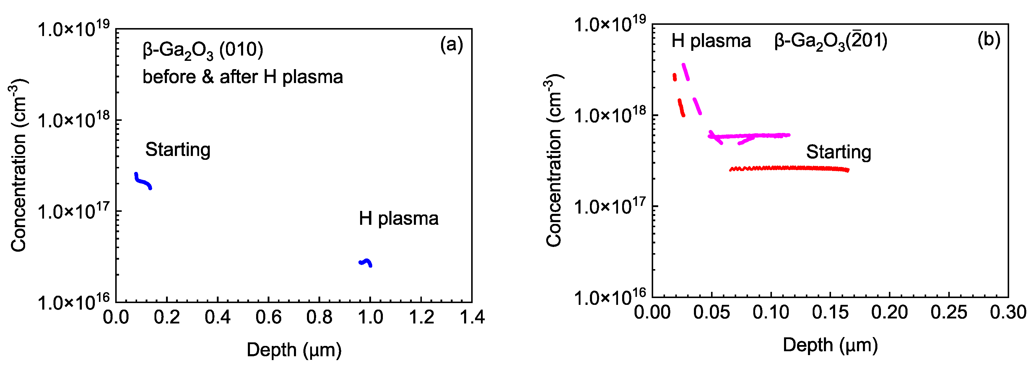
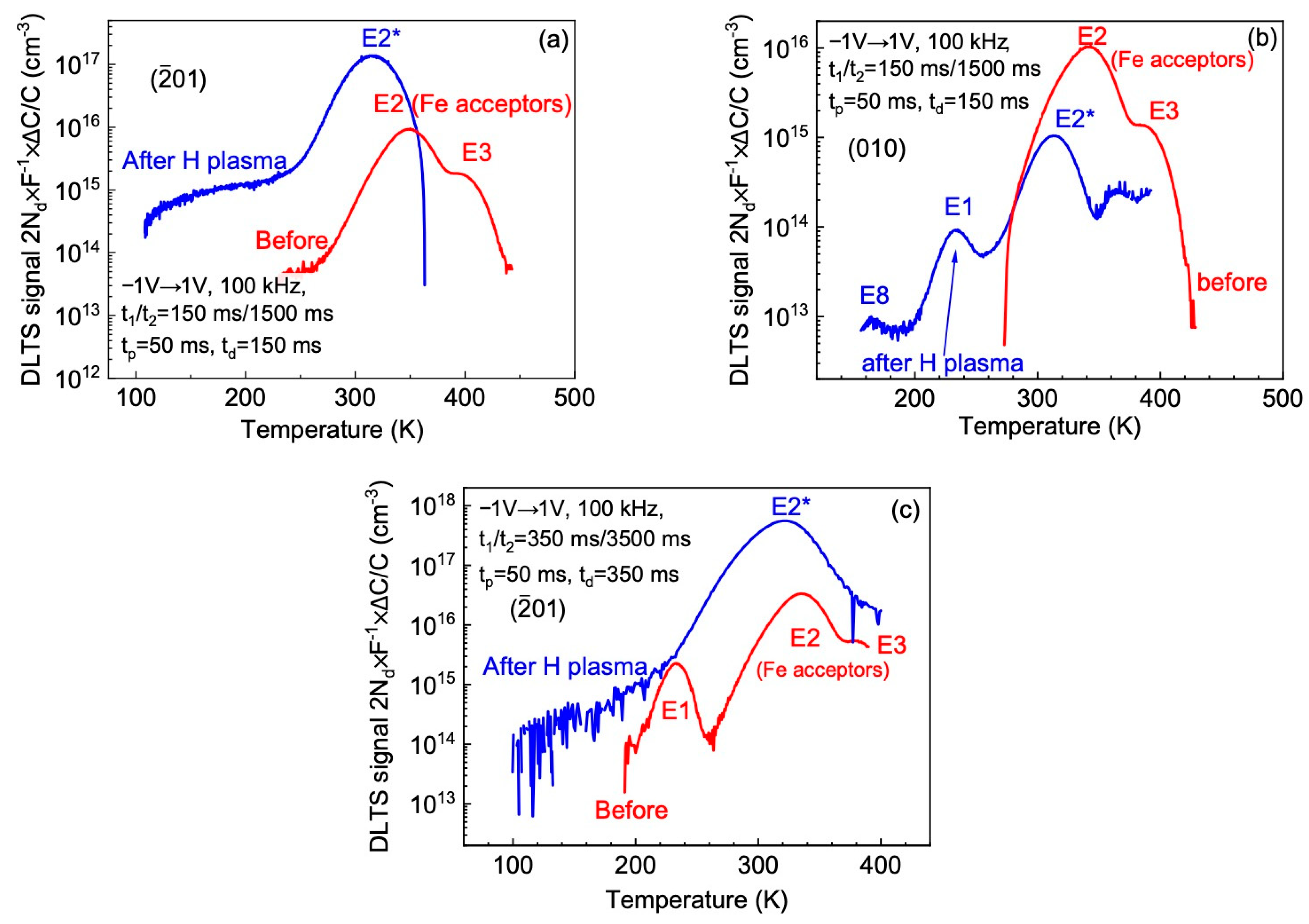
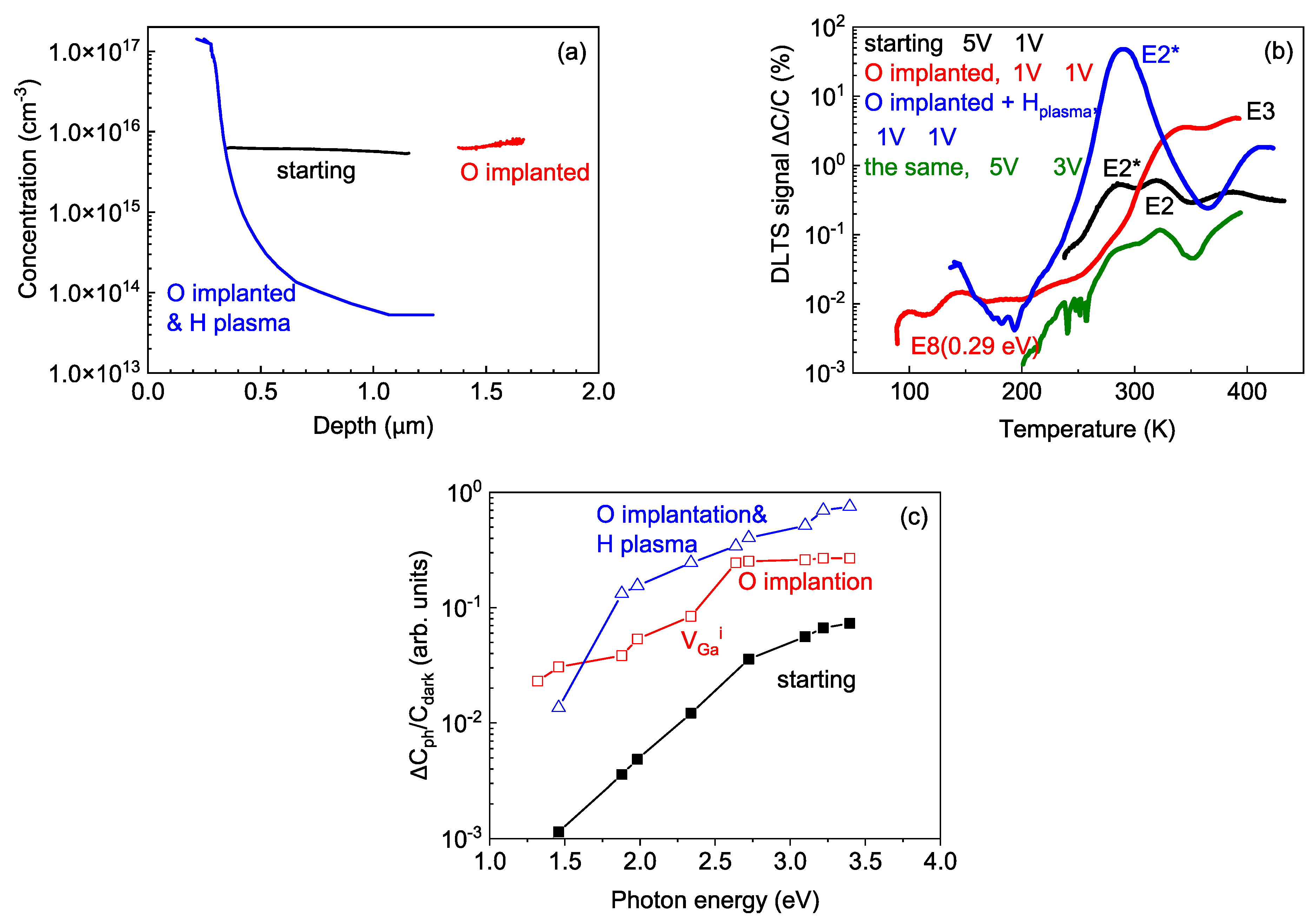
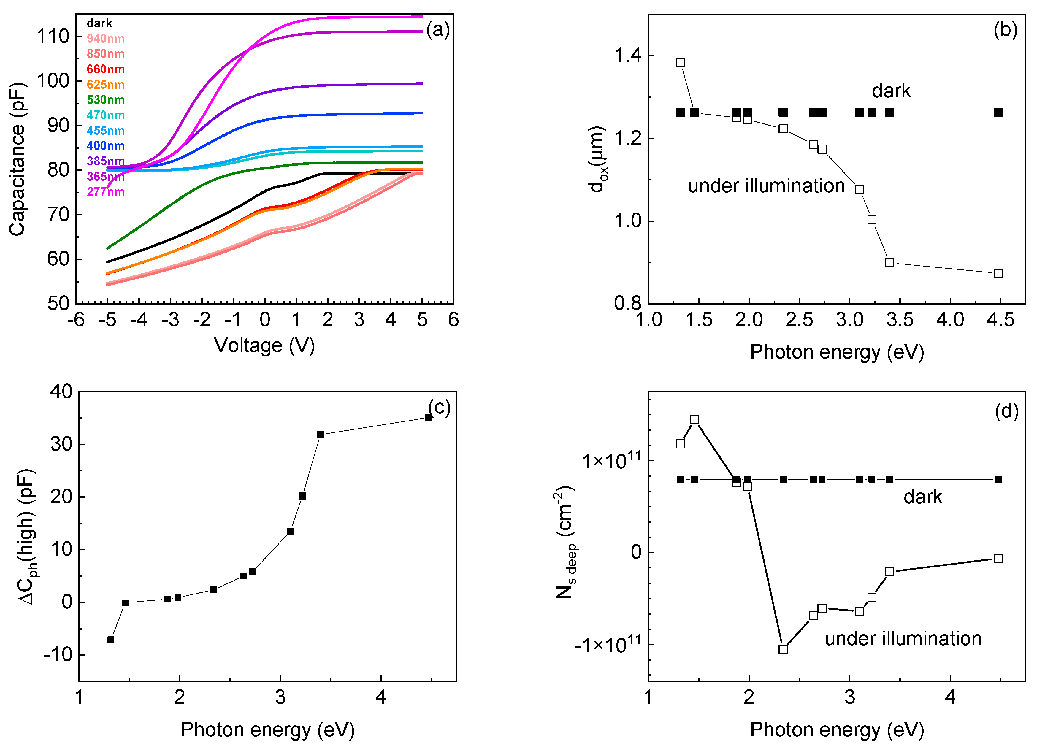
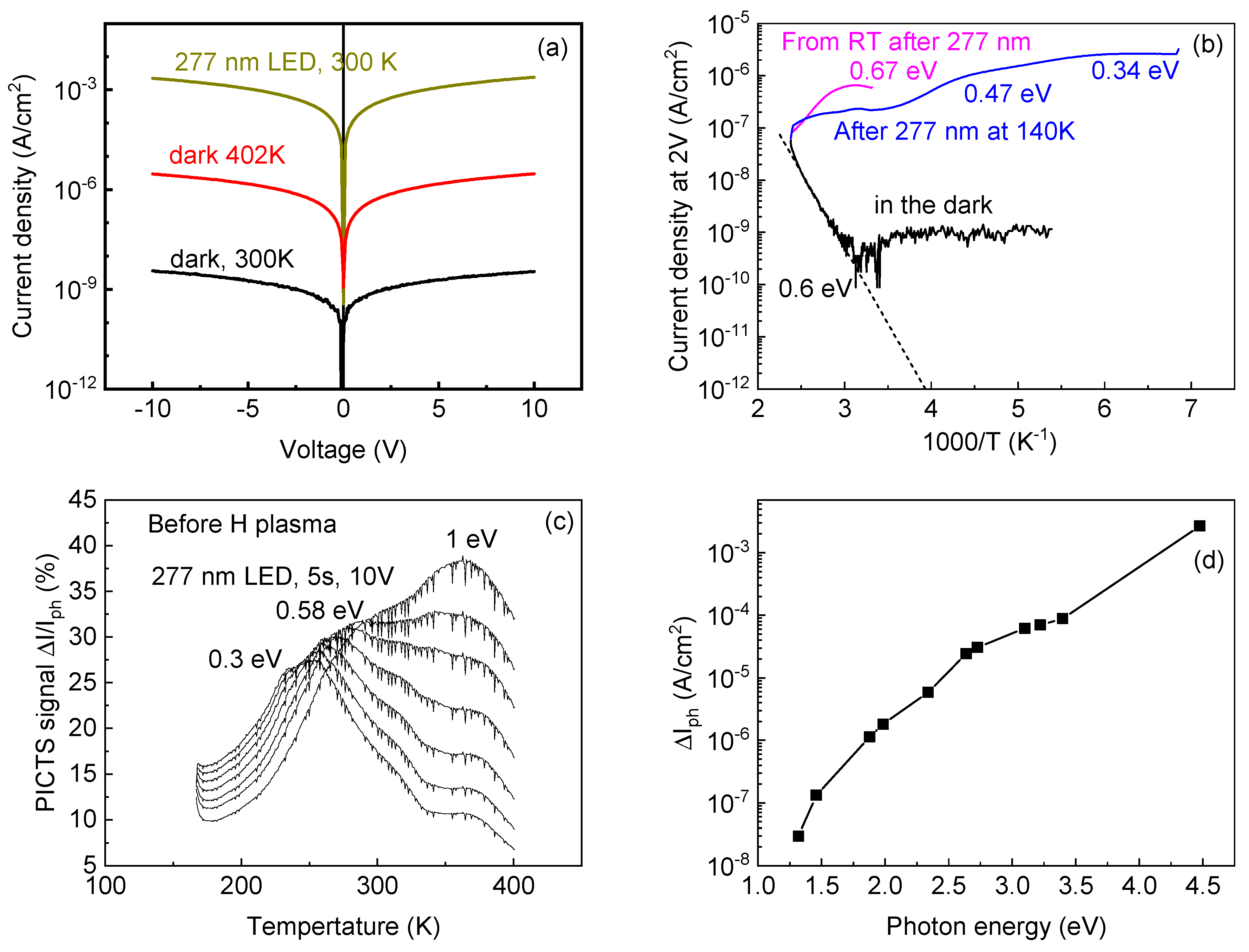
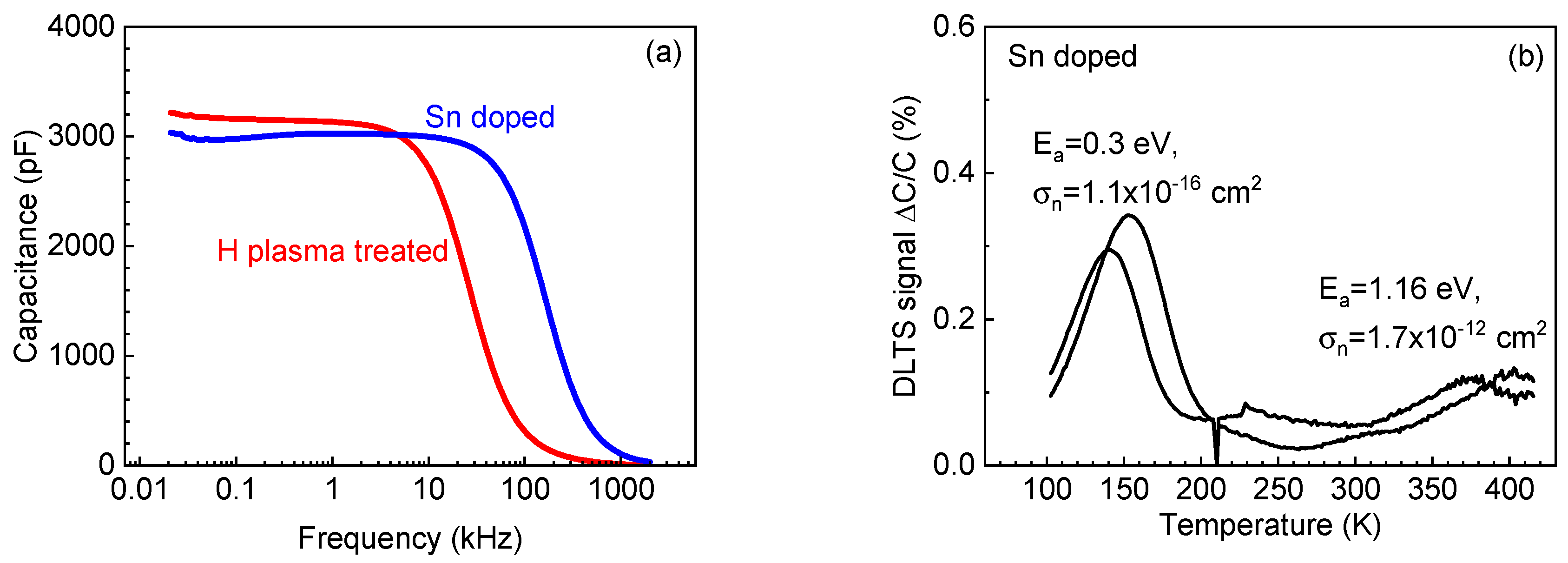
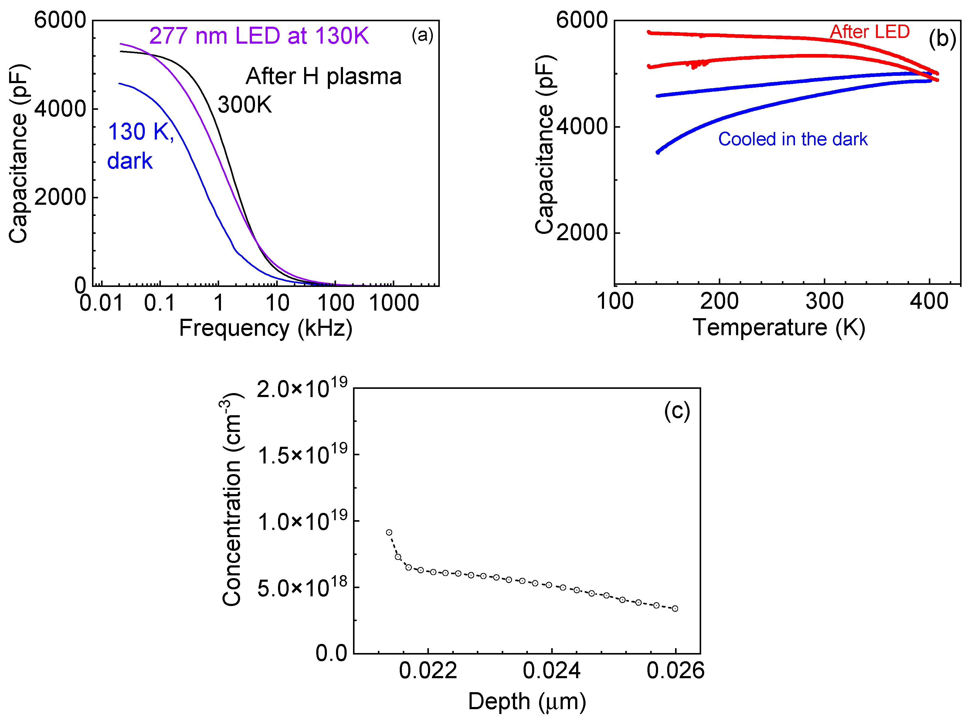
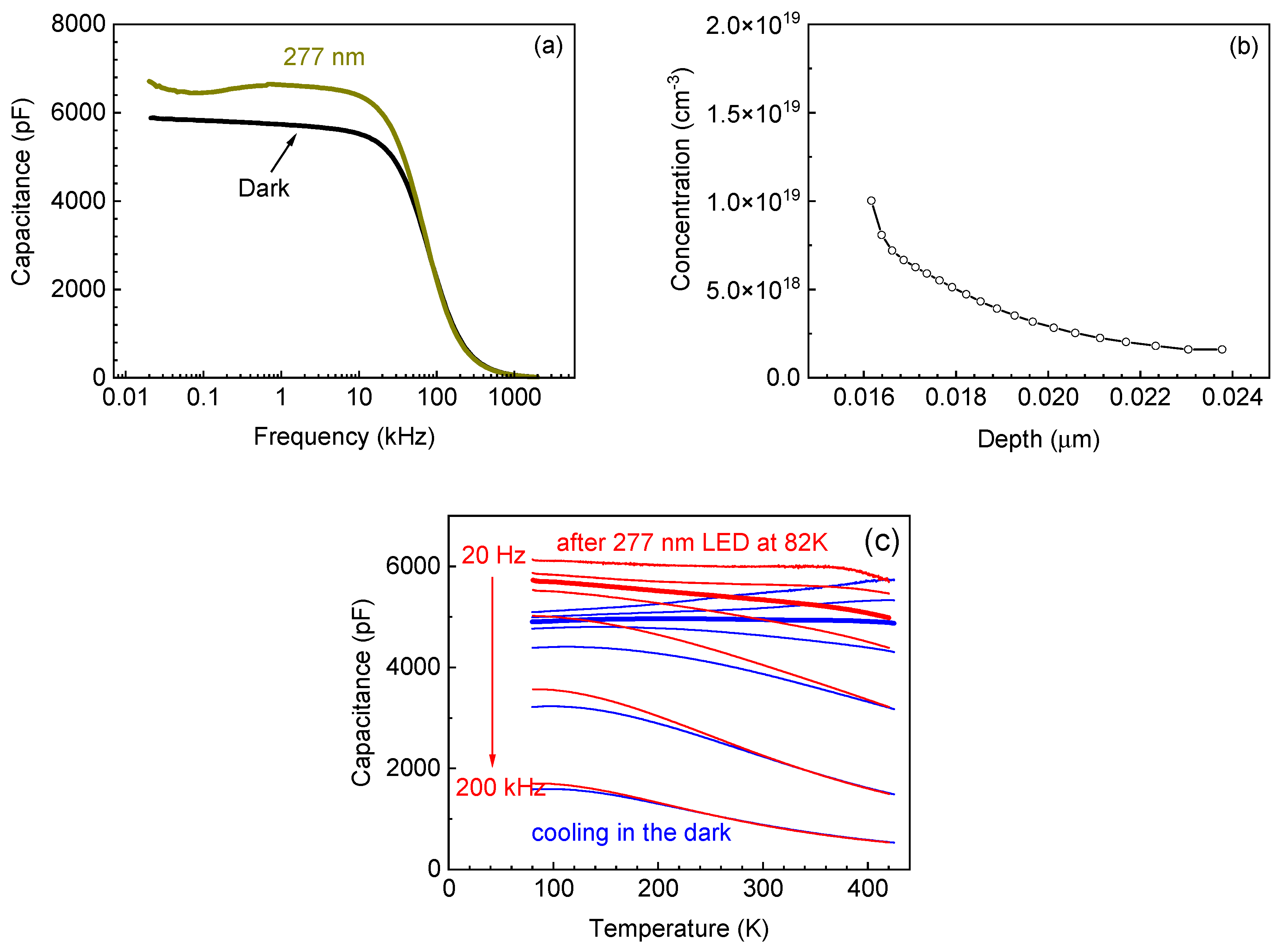

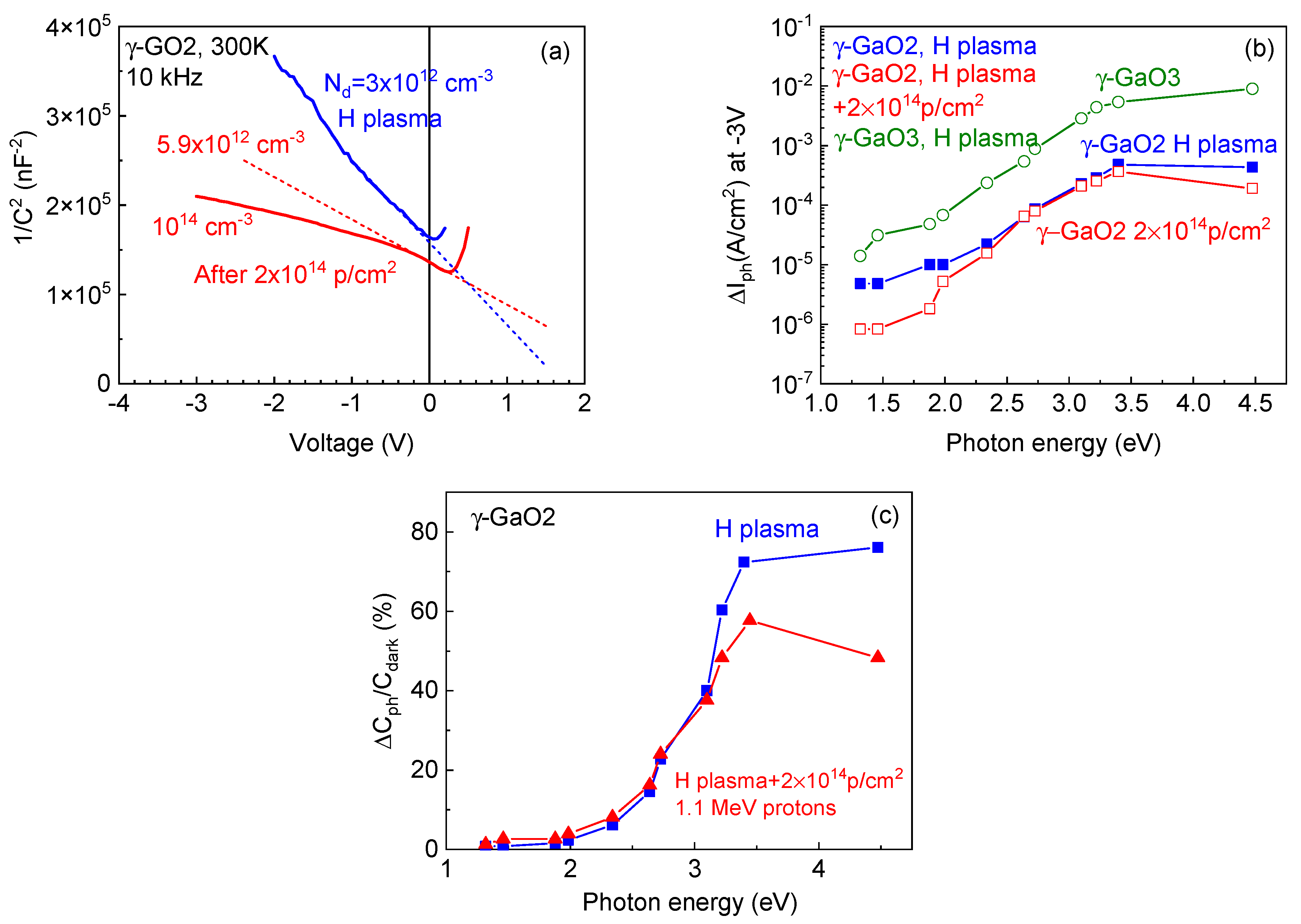
Disclaimer/Publisher’s Note: The statements, opinions and data contained in all publications are solely those of the individual author(s) and contributor(s) and not of MDPI and/or the editor(s). MDPI and/or the editor(s) disclaim responsibility for any injury to people or property resulting from any ideas, methods, instructions or products referred to in the content. |
© 2023 by the authors. Licensee MDPI, Basel, Switzerland. This article is an open access article distributed under the terms and conditions of the Creative Commons Attribution (CC BY) license (https://creativecommons.org/licenses/by/4.0/).