Article

β-Ga2O3 Schottky Barrier Diode with Ion Beam Sputter-Deposited Semi-Insulating Layer

by
Nikita N. Yakovlev
1,
Aleksei V. Almaev
1,2,*,
Bogdan O. Kushnarev
1,
Maksim G. Verkholetov
1,3,
Maksim V. Poliakov
3 and
Mikhail M. Zinovev
4
1
Research and Development Centre for Advanced Technologies in Microelectronics, National Research Tomsk State University, 634050 Tomsk, Russia
2
Fokon LLC, 248035 Kaluga, Russia
3
Institute of Nanotechnology of Microelectronics of the Russian Academy of Sciences, 119991 Moscow, Russia
4
Laboratory of Optical Crystals «LOC LLC», 634050 Tomsk, Russia
*
Author to whom correspondence should be addressed.
Crystals 2024, 14(2), 123; https://doi.org/10.3390/cryst14020123
Submission received: 28 December 2023 / Revised: 16 January 2024 / Accepted: 22 January 2024 / Published: 26 January 2024
(This article belongs to the Special Issue β-Ga2O3: Growth (Bulk, Thin Film, Epitaxy) and Physical Properties)

Abstract

:
Vertical Schottky barrier diodes based on an ion beam sputter (IBS)-deposited β-Ga2O3 film on a single-crystalline ( 2 ¯ 01) unintentionally doped (UID) β-Ga2O3 with a Ni contact were developed. To form ohmic Ti/Ni contacts, the IBS-Ga2O3/UID β-Ga2O3 structures were wet-etched, and an indium tin oxide (ITO) intermediate semiconductor layer (ISL) was deposited on the opposite surface of the UID β-Ga2O3. The IBS-deposited Ga2O3 layer was polycrystalline and semi-insulating. Low leakage currents, rectification ratios of 3.9 × 10⁸ arb. un. and 3.4 × 10⁶ arb. un., ideality factors of 1.43 and 1.24, Schottky barrier heights of 1.80 eV and 1.67 eV as well as breakdown voltages of 134 V and 180 V were achieved for diodes without and with ITO-ISL, respectively. The surface area of the IBS-Ga2O3 film acted as a thin dielectric layer and, together with the preliminary wet etching, provided low leakage currents and relatively high Schottky barrier heights. Diodes with a Schottky barrier based on a Ni/IBS-deposited Ga2O3 film contact were demonstrated for the first time.

1. Introduction

In order to improve the efficiency of electrical equipment, inductive motor controllers and power supplies require the development of power electronics components that differ from Si-based devices by having superior characteristics. β-Ga2O3 is an interesting base material for such devices.
β-Ga2O3 bulk crystals are grown, using a real bulk growth method, from a melt [1,2] and therefore have a better crystalline quality in comparison with the other electronics with technology-relevant wide-bandgap semiconductors: SiC [3], GaN [4] and AlN [5]. Today, the typical dislocation density of bulk β-Ga2O3 single crystals grown via the vertical Bridgman method, the edge-defined film-fed growth (EFG) method, the floating zone process and other melt-growth techniques is ~103–104 cm−2 [6,7,8,9,10,11] versus 105–107 cm−2 for vapor- and solution-grown GaN [12,13,14,15,16,17,18,19,20,21] and SiC [22,23,24,25], correspondingly. It is worth noting that heteroepitaxy also allows the deposition of layers of different Ga2O3 polymorphs with high structural quality and low dislocation density [26,27].
In addition, the feasibility of using β-Ga2O3 is due to its ultra-large bandgap energy Eg = 4.5 eV without alloying like AlGaN, which determines the theoretical breakdown field strength of εc = 8 MV/cm, the ability to withstand high temperatures, and the strong dependence of the electrical properties on the presence and concentration of impurities [28]. Estimates have shown that the Baliga figure of merit (BFOM) of β-Ga2O3 is approximately 3000 times higher than that of Si. In addition, β-Ga2O3 significantly outperforms GaN and SiC in these parameters. The ability to dope β-Ga2O3 with shallow donors up to a concentration of 1021 cm−3 is a significant advantage over the ultra-wide bandgap semiconductors Al0.7Ga0.3N and diamond [27,29]. In addition, β-Ga2O3 is characterized by high thermal and chemical stability.
The first publications devoted to power devices based on β-Ga2O3 appeared in 2010 [28,30,31,32]. To date, Schottky barrier diodes (SBDs) and field effect transistors (FETs) have been developed in a variety of designs, with lateral and vertical transport [28,33,34]. In addition, among the known five different phases of gallium oxide [35], which are widely studied mainly for the development of various detectors [36,37], β-Ga2O3 is the most thermodynamically stable polymorph, which significantly expands the methods of material modification [38]. In addition to power electronics, stable β-Ga2O3 and metastable α- and κ(ε)-Ga2O3 polymorphs are being actively investigated for the development of solar-blind shortwave UV detectors and gas sensors.
SBDs based on β-Ga2O3 with a breakdown voltage Vbr of 2–4 kV have been successfully developed within the last few years [39,40,41]. The vertical SBDs are of large interest due to the relative simplicity of the fabrication technology, the ability to employ a variety of β-Ga2O3 modification methods and designs to optimize the SBDs, as well as the ability to handle higher currents and powers. Despite the promising results achieved worldwide, further research is needed to improve the performance of β-Ga2O3-based SBDs and to modify their design. In addition, there are difficulties in making ohmic contacts to β-Ga2O3. Promising approaches for modifying β-Ga2O3 to improve the parameters of the SBDs are, e.g., the formation of an ISL, preliminary wet-etching of the semiconductor surface, additional annealing procedures and the formation of gate dielectric layers [42,43,44,45,46,47]. The deposited highly conductive indium tin oxide (ITO) thin film, followed by annealing, is an intermediate semiconductor layer that is used to form an ohmic contact with low contact resistance and high temperature stability [48,49]. In this work, such approaches were employed to fabricate SBDs based on β-Ga2O3. A β-Ga2O3 layer deposited by IBS, followed by high-temperature annealing was used as a gate dielectric layer for the first time. An ITO ISL was deposited followed by a rapid thermal annealing (RTA) to form an ohmic contact. The effect of etching in HCl solution followed by treatment in H2O2 on the device performance of the β-Ga2O3-based SBDs was investigated in detail.
IBS deposition is characterized by the highest energies of the particles involved in the formation of thin films, as well as a large number of parameters affecting the sputtering process and the ability to achieve a higher vacuum in the operating mode [50,51,52,53]. This allows a more subtle variation in the electrically conductive, structural, optical, mechanical and other properties of the films during the deposition process and allows us to obtain more homogeneous layers in terms of thickness and composition over larger areas of the substrates. Thin films deposited via the IBS method are characterized by high adhesion, a dense structure, high stoichiometry and high purity. Films of the α- and β-Ga2O3 phases can be deposited by IBS by varying the parameters of the IBS deposition process [53]. The possibility of depositing metastable κ(ε)-Ga2O3 films has also been suggested. In this work, the IBS-deposited β-Ga2O3 film was used for the first time to develop an electronic device.

2. Experimental Methods and Materials

Unintentionally doped β-Ga2O3 commercial wafers (Tamura Corp., Tokyo, Japan) with a surface orientation of ( 2 ¯ 01), a thickness of 650 µm and a donor net concentration Nd of ~1017 cm−3 were used as a substrate in the fabrication of vertical Schottky barrier diodes.
A Ga2O3 film of ~500 nm in thickness was homoepitaxially grown via the IBS method on the surface of UID β-Ga2O3 ( 2 ¯ 01) wafers. This film is denoted as IBS-Ga2O3. The IBS synthesis process was carried out using an Aspira-200 (Belarus) system equipped with a ring beam ion source. The sputtered target was a 5″ disc of compressed Ga2O3 powder with a purity of 99.995 wt.% (Lanhit LLC, Moscow, Russia). The Ga2O3 powder was pressed under a load of 60 tons for 3 h at room temperature (RT). The diameter of the ion beam focused on the target was ~25 mm. UID β-Ga2O3 wafers were cleaned using an auxiliary ion source at ~40 W source power and ~150 eV ion energy for 10 min in the chamber before the deposition of IBS on the Ga2O3 film. The temperature of the UID β-Ga2O3 wafers during the deposition of IBS on the Ga2O3 film was 250 °C. Ar and O2 of high purity (99.995 vol.%) were used as working gases in the system. The Ar/O2 flow ratio was ½ with a total flow of 30 cm3/min. The gas pressure in the chamber during the IBS-Ga2O3 films deposition was 3.750 μTorr. The deposition time of an IBS-Ga2O3 film with a thickness of ~500 nm was within 8 h. The IBS Ga2O3/UID β-Ga2O3 structures were annealed at a temperature of Tann = 800 °C in air atmosphere for 30 min.
Some of the IBS-Ga2O3/UID β-Ga2O3 structures were etched in a 10% HCl solution for 5 min at RT, followed by treatment in H2O2 for 5 min at T = 85 °C. Wet etching was used to prepare the surface of IBS Ga2O3/UID β-Ga2O3 structures prior to the deposition of contacts. Continuous Ti layers of 20 nm in thickness and Ni of 100 nm in thickness were then deposited on the surface of UID β-Ga2O3 using vacuum thermal sputtering at a pressure of ~0.750 μTorr. The structure was subjected to RTA at Tann = 400 °C in vacuum for 1 min after deposition of the Ti/Ni layers. A Ni anode with a diameter of 1 mm and a thickness of 100 nm was deposited on the surface of the IBS Ga2O3 film by means of vacuum thermal sputtering through a shadow mask.
For the second part of the IBS Ga2O3/UID β-Ga2O3 structures, an ITO film was deposited on the β-Ga2O3 surface via radio frequency magnetron sputtering of an oxide target in Ar/O2 plasma using an Edwards A-500 (UK) system. Furthermore, the IBS Ga2O3/UID β-Ga2O3 structures were treated in acetone, isopropyl alcohol, and deionized water before the ITO film deposition. The IBS Ga2O3/UID β-Ga2O3 structure was not specially heated during the ITO film deposition. The working pressure and power of the system were 5.250 mTorr and 70 W, respectively. The oxygen concentration in the O2 + Ar mixture was 10 ± 0.5 vol.%. The thickness of the ITO films was within 210–260 nm for 20 min deposition time. A Ti/Ni cathode was deposited on the surface of the ITO film, and a Ni anode was deposited on the surface of the IBS Ga2O3 film. The structure was subjected to RTA at Tann = 400 °C in vacuum for 1 min after deposition of the ITO film and the Ti/Ni layers.
Thus, two types of SBDs with vertical electron transport and different ohmic contacts were fabricated. The series of samples without an ITO layer is denoted as SBD A, and the series of samples with an incorporated ITO layer is denoted as SBD B. Schematic images of the fabricated SBDs are illustrated in Figure 1.
In addition, the electrically conductive characteristics of the structures based on IBS-Ga2O3 and ITO films deposited on sapphire substrates in the modes described above were investigated. On the surface of the films, symmetrical Pt contacts were deposited by means of direct current magnetron sputtering.
A focused ion beam (FIB) scanning electron microscope (SEM) and Helios G4 CX nanomanipulators (Thermo Fisher Scientific Inc., Waltham, MA, USA) were used to prepare lamellae of samples for transmission electron microscopy (TEM) analysis. The sample preparation method is described in detail in Refs. [54,55]. The preparation of the samples for TEM by means of the FIB SEM technique involved the following steps:
  • Choosing of the samples region to produce the lamella and its orientation;
  • Deposition of a Pt layer to protect the samples surface against ion etching by means of a gas injection system at an accelerating voltage of U1 = 30 kV and a current of I1 = 24 pA;
  • Formation of two trapezoidal depressions on either side of the protective Pt layer by means of an FIB at U1 = 30 kV and I1 = 0.23 pA;
  • Cutting of lamellae along the perimeter by means of an FIB at U1 = 30 kV and I1 = 0.79 pA;
  • Bringing and welding the Pt probe of the nanomanipulator to the lamella and then removing it from the sample;
  • Moving the lamella with the nanomanipulator onto the grid for TEM and then welding it with Pt using a gas injection system;
  • FIB thinning of a lamella welded to a grid at U1 = 30 kV and I1 = 80 pA;
  • Final polishing of the lamella surface with an ion beam at U1 = 30 kV and I1 = 24 pA.
Cross-sectional images of the annealed IBS-Ga2O3/UID β-Ga2O3 structures were examined using the Jeol JEM 2100 PLUS TEM (JEOL USA, Inc., Peabody, MA, USA) equipment at an accelerating voltage of 200 kV in a bright field (BF) mode. The elemental composition of the films was determined by the BF-TEM mode by means of a Jeol EX-24261M1G5T (JEOL USA, Inc., Peabody, MA, USA) energy dispersive X-ray (EDX) spectroscopy analyzer at a beam current of 1 nA.
Room temperature transmission spectra of the UID β-Ga2O3 wafers, IBS Ga2O3/UID β-Ga2O3 and ITO/UID β-Ga2O3 structures were measured using a combined DH-2000 radiation source based on deuterium and tungsten halogen lamps and an Ocean Optics spectrometric system (Ocean Insight, Orlando, FL, USA). The DH-2000 radiation source provides stable radiation in the wavelength range of Δλ = 190–2500 nm. The transmitted radiation was focused by collecting optics and transmitted via optical fiber to the input of the Ocean Optics spectrometers. The Ocean Optics USB 2000+ spectrometer with a wavelength range of 320–517 nm and the Ocean Optics Flame spectrometer with a wavelength range of 200–850 nm were used. Measurements were controlled using Ocean View 1.5.0 software. The wavelength λ was measured with an optical resolution of 1 nm.
The electrically conductive characteristics of the structures under dark conditions were measured in a sealed Nextron MPS-CHH (Nextron Corp., Busan, Republic of Korea) chamber equipped with microprobes. The samples were placed on a ceramic table which allowed for heating of the samples from RT to T = 750 °C with an accuracy of ±0.1 °C. The atmosphere in the chamber was pure dry air. Pure dry air was pumped throughout the chamber containing the samples for 5 min prior to the measurements of the electrically conductive characteristics to eliminate the influence of the atmosphere. A special generator was used as a source of pure dry air. The flow rate of the pure dry air was 1000 cm3/min. The I-V (J-V) and C-V characteristics were measured using a Keithley 2636A (Keithley Instruments LLC, Cleveland, OH, USA) source meter and an E4980A RLC (Agilent Technologies, Santa Clara, CA, USA) meter, respectively, where I is the current, J is the current density, C is the electrical capacitance, and V is the applied voltage. A Keithley 2636A source meter allows us to measure extremely low currents, up to 10−12 A. The measurements of the I-V (J-V) and C-V characteristics were carried out in an automated mode using a program developed on the basis of the Labview platform.

3. Results and Discussion

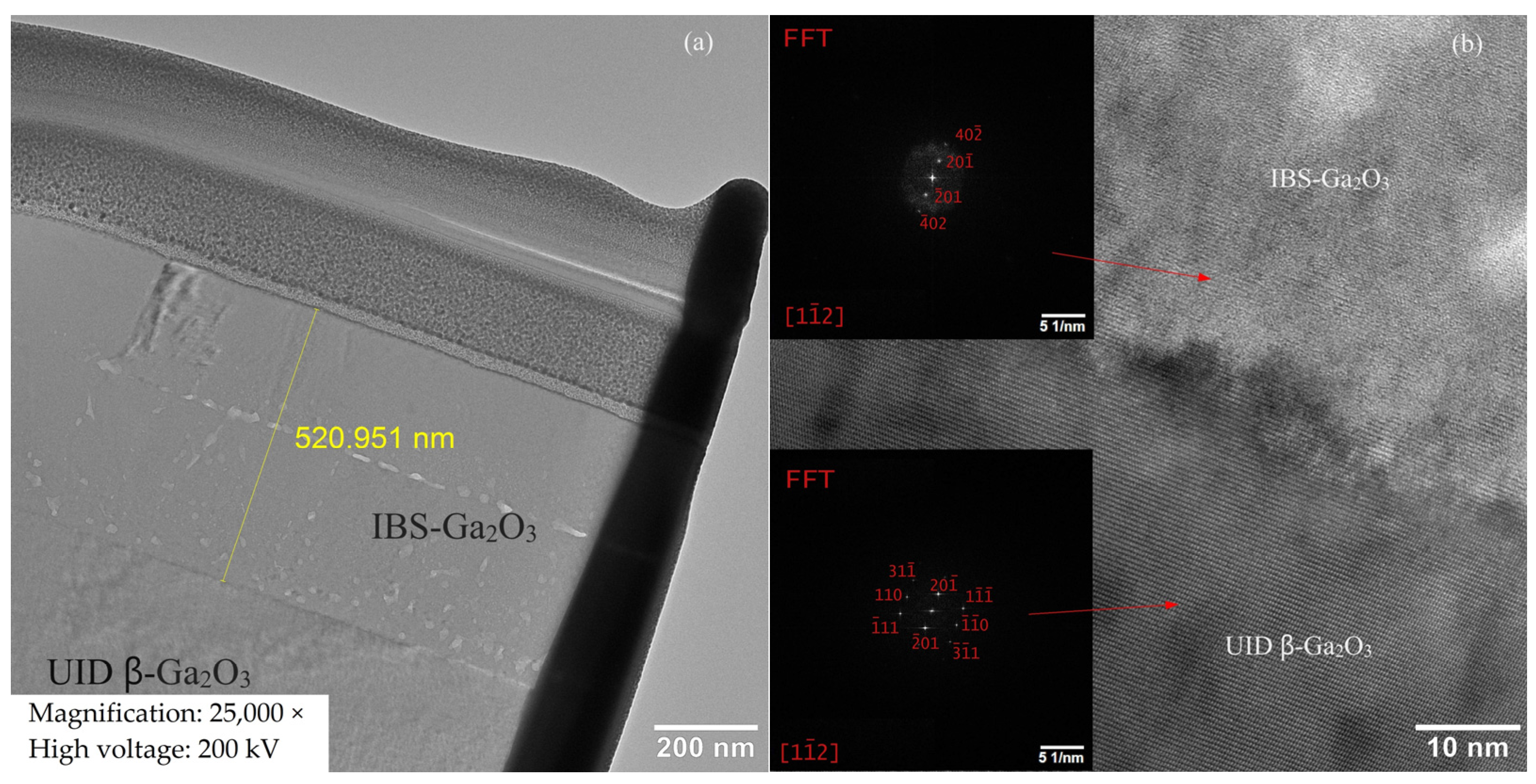
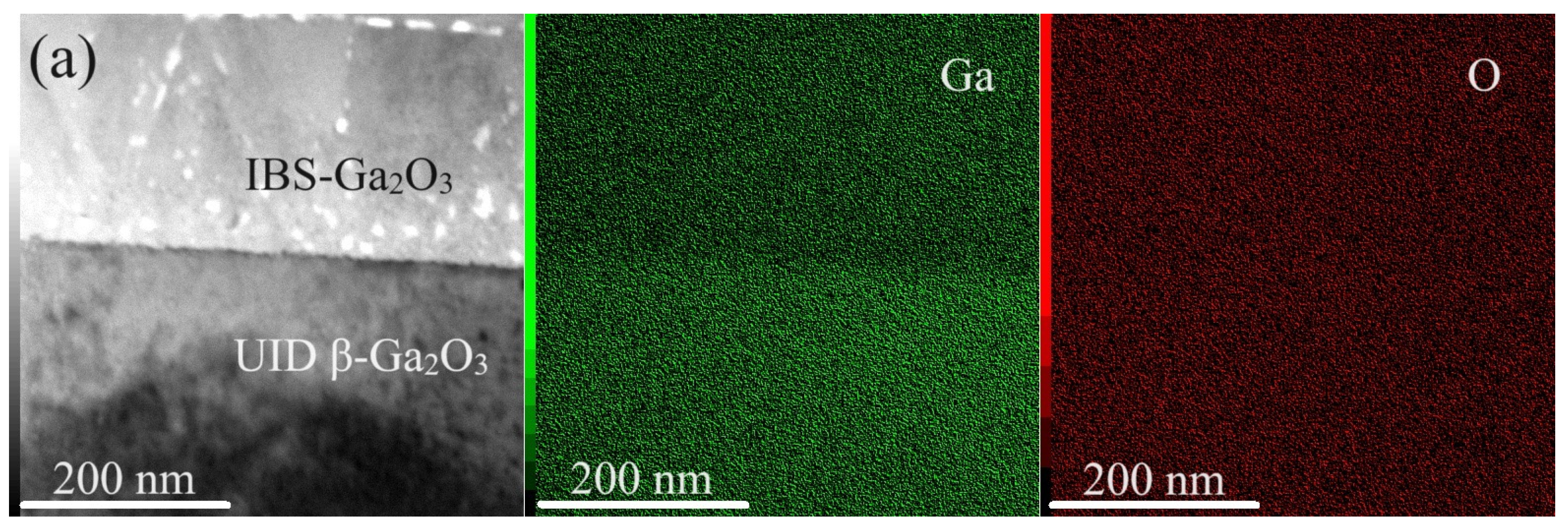
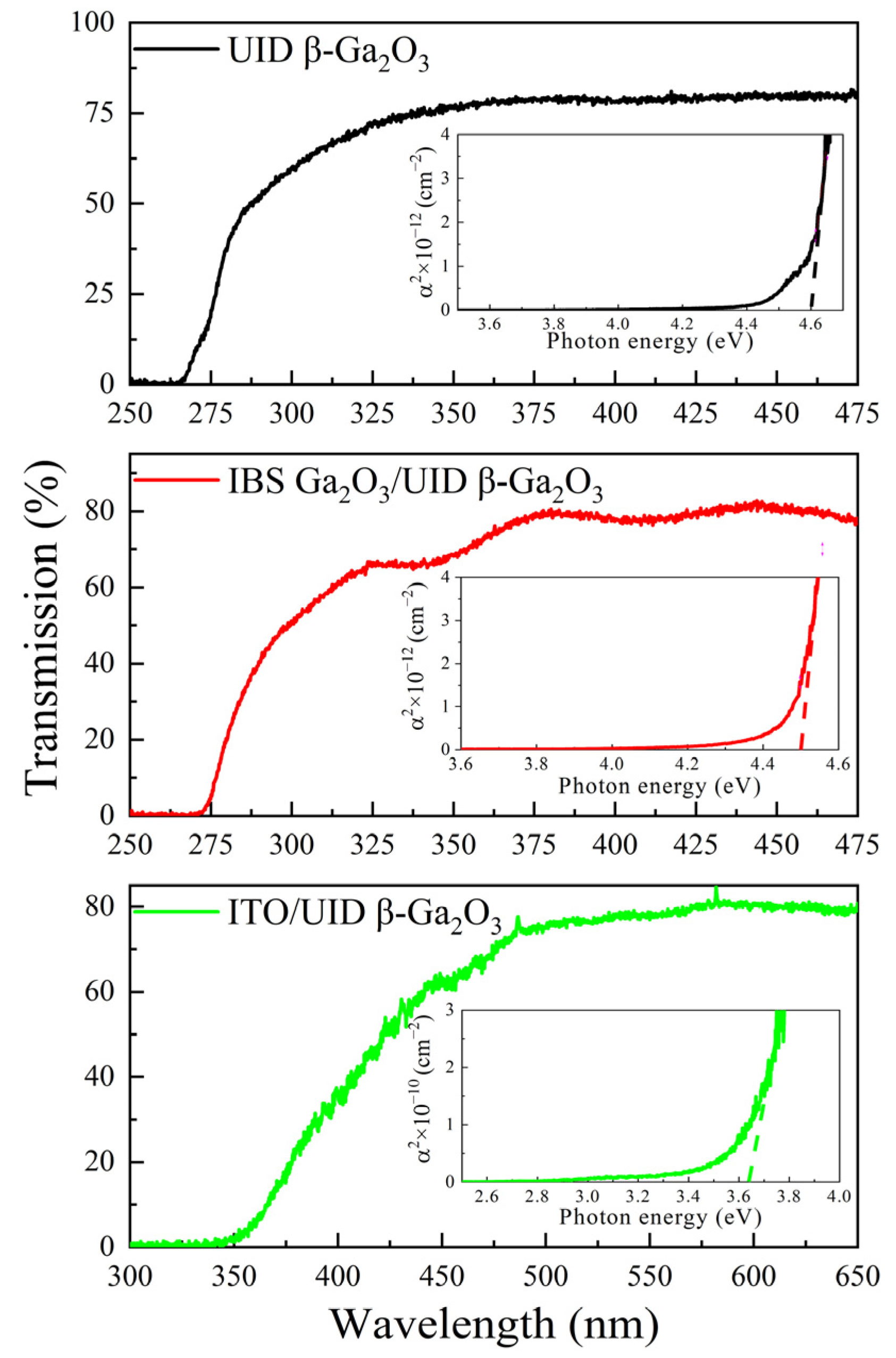
3.1. Structural Properties of IBS Ga2O3/UID β-Ga2O3 and ITO/UID β-Ga2O3 Structures

A typical TEM image of the IBS Ga2O3/UID β-Ga2O3 structure, illustrated in Figure 2a, shows an abrupt interface. The thickness of the IBS Ga2O3 film is ~521 nm according to the SEM. Figure 2b shows an HRTEM image of an annealed IBS Ga2O3/UID β-Ga2O3 structure near the interface. The interplanar distances d for the UID β-Ga2O3 substrate and the IBS Ga2O3 film were determined via the fast Fourier transform (FFT) method based on the phase contrast. The IBS-Ga2O3 film, like the UID β-Ga2O3 substrate, is a relevant monoclinic β-Ga2O3 phase with a structural group of C2/m(12). The d corresponding to the reflections of the ( 2 ¯ 01), (− 1 ¯ 10), ( 1 ¯ 11) and (31 1 ¯ ) planes of the β-Ga2O3 phase (ICSD # 83645) are 0.468 nm, 0.295 nm, 0.267 nm and 0.234 nm, respectively. The IBS-Ga2O3 film, which is in contact with the Ni anode, is polycrystalline and, as shown below, is semi-insulating. We believe this is due to the nature of the film deposition process [51,52,53]. It is worth noting that such relatively thick β-Ga2O3 films deposited via the IBS method on UID β-Ga2O3 substrates and annealed at the conditions described above are being studied for the first time. According to Refs. [51,52,53], it was expected that IBS β-Ga2O3 films would be monocrystalline and of high structural quality.
TEM EDX maps of the IBS Ga2O3/UID β-Ga2O3 interface and EDX spectra of the IBS-Ga2O3 and UID β-Ga2O3 near the IBS-Ga2O3/UID β-Ga2O3 interface are depicted in Figure 3a,b, respectively. According to the EDX, the Ga and O contents in the IBS Ga2O3 films are ~42 at.% and ~58 at.%. Thus, a reduced content of oxygen atoms in the IBS-deposited layer is observed. No peaks corresponding to other elements are detected in the EDX spectra. The Sn content in the ITO films is determined to be ~5 at.% according to the EDX.
Transmission spectra of the UID β-Ga2O3 wafers, IBS Ga2O3/UID β-Ga2O3 and ITO/UID β-Ga2O3 structures are exhibited in Figure 4. The transmission values of the UID β-Ga2O3 wafers and IBS Ga2O3/UID β-Ga2O3 structures in the range of λ = 350–475 nm are above 75%. A sharp drop in the transmittance is observed at short λ due to the band-to-band absorption of photons. An analysis of the absorption edge of the samples showed that the Eg is 4.6 eV and 4.5 eV for the UID β-Ga2O3 and IBS Ga2O3/UID β-Ga2O3 structures, respectively. Interference phenomena are observed at the IBS Ga2O3/UID β-Ga2O3 interface. The thickness of the IBS Ga2O3 film determined from an analysis of the position of the interference maxima is 518 nm and is close to the declared value and result of TEM. The transmission spectra of the ITO/UID β-Ga2O3 structures are determined by the ITO film. The transmittance values of these structures are above 75% within the range of λ = 500–650 nm. A decrease in the transmittance of the ITO/UID β-Ga2O3 structures is observed in the range of λ = 350–450 nm due to the band-to-band absorption of photons. The Eg of the ITO film is determined to be 3.6 eV.

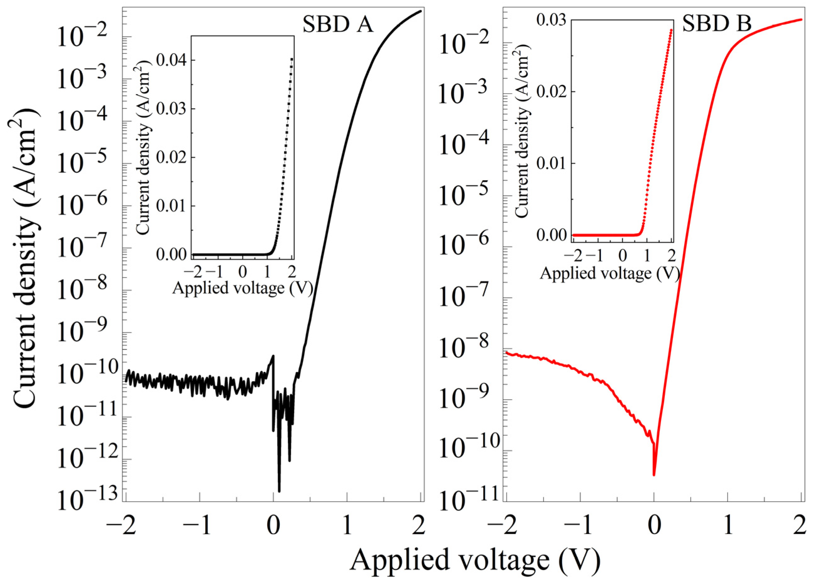
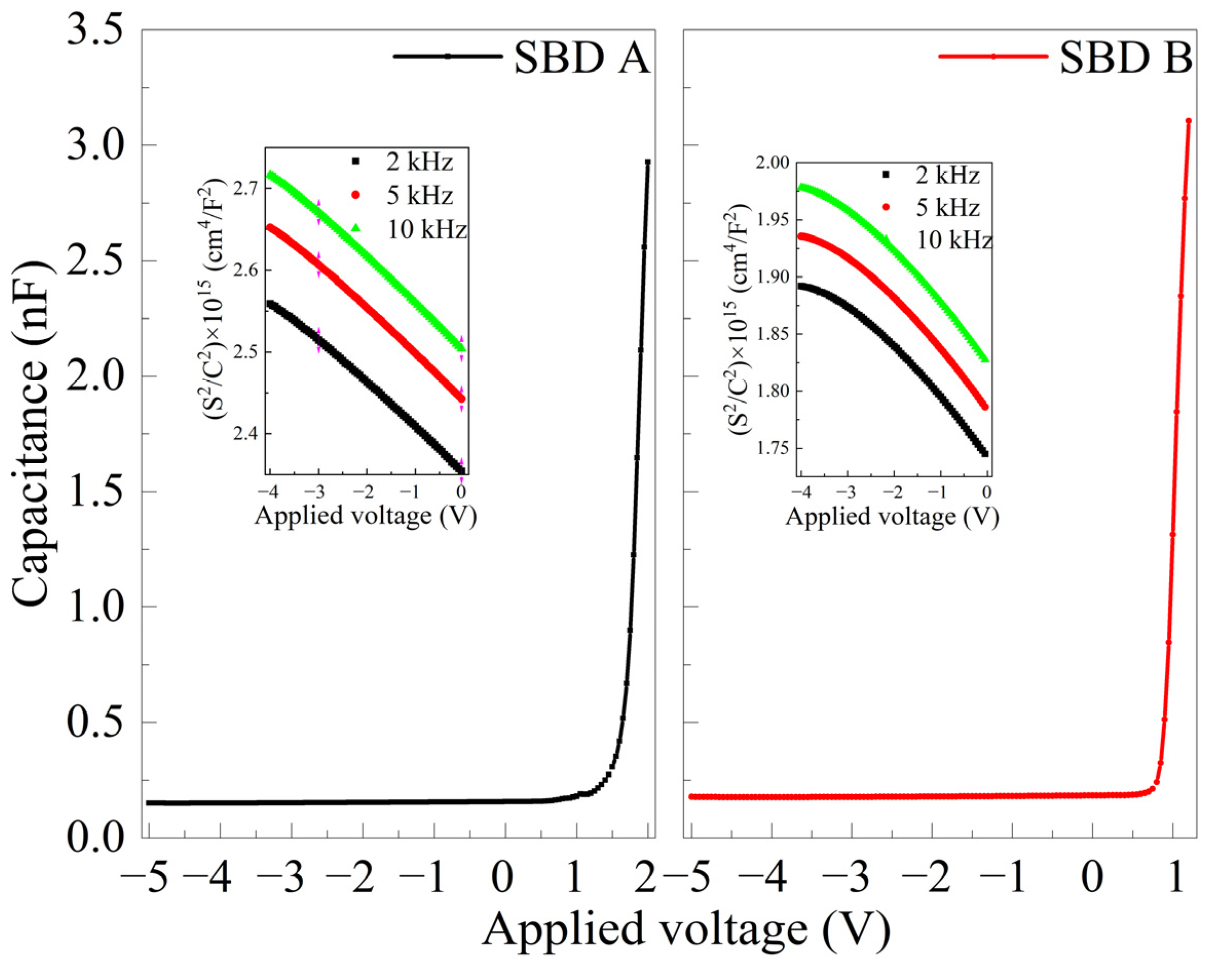
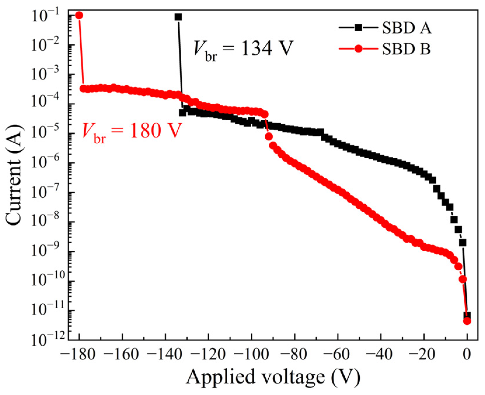
3.2. Electrically Conductive Characteristics of Diodes Based on IBS Ga2O3/UID β-Ga2O3 and IBS Ga2O3/UID β-Ga2O3/ITO Structures with Ni Gate

We used UID β-Ga2O3 commercial wafers grown via the EFG technique as substrates. During the growth process, donor type defects are formed in the β-Ga2O3 wafer, resulting in a donor concentration of the order of ~1017 cm−3 [56]. The electrical properties and defects of EFG UID β-Ga2O3 are summarized in Refs. [57,58,59].
Preliminary measurements showed that the IBS-deposited Ga2O3 film is characterized by semi-insulating behavior at RT and that ITO is highly conductive, despite the relatively low annealing temperature. The resistance of the IBS Ga2O3 film at RT is above the measurement limit. It is possible to measure the I-V characteristics of the IBS Ga2O3 film with Pt contacts at T = 600 °C. The resistivity of the IBS Ga2O3 film is determined to be 1.24 × 10⁷ Ohm × cm at this temperature. The resistivity of the ITO film at RT is 0.035 Ohm × cm.
The experimental dependencies of the current density on the applied voltage of the diodes in the range from –2 V to 2 V at RT are depicted in Figure 5. Evidently, both types of diodes demonstrate rectifying characteristics. The rectification ratios at ±2 V are 3.9 × 10⁸ arb. un. and 3.4 × 10⁶ arb. un. for SBD A and SBD B, respectively. An analysis of the J-V characteristics was carried out to estimate the ideality coefficient n, the saturation current density of the diodes Js and the height of the potential barrier Φb. According to the thermionic emission (TE) model, the direct branch of the J-V characteristics can be approximated by the following expression [6,41]:
J = Js(exp[eV/(nkT)] − 1),
where e is the electron charge; k is the Boltzmann constant; and T is the absolute temperature of the semiconductor. The ideality coefficient was determined from the analysis of the linear portion of the J-V characteristics using the following formula:
ln(J/Js) = eV/(nkT).
The Js was obtained by extrapolating ln(J/Js) to the point of V = 0. According to theories expressed in [6,41],
Js= A*T2 × exp(−eΦb/(nkT)),
where A* is the Richardson constant. A* = 33.65 A/(cm−2 × K−2) according to estimates from experimental data at the effective mass of electrons mn* = 0.28m0, where m0 is the mass of an electron in vacuum. Using expression (3), Φb can be estimated using the following formula:
Φb = ln(A*T2/Js)×(nkT/e),
The calculated n, Js and Φb, and other experimental parameters of the diodes are summarized in Table 1.
The C-V characteristics of the SBD A and SBD B measured at different amplitudes of the signal u and frequencies f are illustrated in Figure 6. The largest changes in the C-V characteristics are observed at u = 100 mV and f = 10 kHz (shown in Figure 6). Nd was determined via an analysis of the C-V characteristics in the coordinates of S2/C2 vs. V by means of the following formula:
Nd = 2/(eεε0b),
where b is the slope of the reverse branch of the C-V characteristics in the coordinates of S2/C2 vs. V (inset of Figure 6). The C-V characteristics obtained are typical of SBD. The Nd for SBD A and SBD B is (1.7–3.1) × 1017 cm−3. Meanwhile, the value of b did not change with f.
The values of leakage current densities obtained are in agreement with the vast majority of experimental works on Schottky diodes based on Ni/β-Ga2O3 [1,6,60]. It should be noted that Schottky diodes based on Ni/β-Ga2O3 and Pt/β-Ga2O3 are currently under extensive investigation. Even lower values of leakage current densities are not yet achievable due to imperfections in the surface structure of β-Ga2O3 crystals, imperfections in the methods of preparing the semiconductor surface prior to the deposition of contacts, and the effects of the concentrating electric field. It should be noted that for diodes based on EFG β-Ga2O3, no obvious relationship between dislocations and the leakage current has been found [60].
The breakdown voltages (Vbr) of the SBD A and SBD B (see Figure 7) are determined to be 134 V and 180 V, respectively. The low Vbr values are probably due to the poor quality of the ohmic contact. The SBD A are characterized by higher values of n, Φb and the rectifier ratio as well as by low Js. However, n for the SBD B is close to 1. In addition, these structures are characterized by a higher Vbr. For an ideal Schottky contact based on Ni/β-Ga2O3, Φb = ΦM − χs [6] and should correspond to 1.15 eV, where ΦM is the work function of the metal and χs is the electron affinity of the semiconductor. For Ni, ΦM = 5.15 eV, and for β-Ga2O3, χs = 4.00 eV. The experimental and theoretical values of Φb are close to or higher than those reported in the literature [6,44]. The structures studied are characterized by significantly high Φb compared to the literature data [1,6]. We suppose the increase in Φb and the decrease in Js is facilitated by the presence of an IBS Ga2O3 layer between the Ni anode and the UID β-Ga2O3. The IBS Ga2O3 film has a polycrystalline structure and demonstrates semi-insulating behavior. Th surface area of this layer acts as a thin dielectric layer, the presence of which leads to an increase in Φb. A similar increase in Φb is typical for the metal–insulator–semiconductor (MIS) diodes [61]. Pre-etching of the structure in an HCl solution followed by treatment in H2O2 also results in higher Φb values of the SBD A. Such a treatment was employed to increase the Φb for a Schottky contact based on β-Ga2O3 and various metals [44]. It has been suggested that this treatment reduces the concentration of oxygen vacancies in the near-surface region of the semiconductor and prevents Fermi level pinning.

4. Conclusions

The development of vertical Schottky barrier diodes based on a contact of Ni and β-Ga2O3 film deposited by ion beam sputtering on single-crystalline ( 2 ¯ 01) unintentionally doped β-Ga2O3 was demonstrated, and their properties were studied. The IBS Ga2O3/UID β-Ga2O3 structures were wet-etched in HCl solution followed by a treatment in H2O2 before forming the ohmic Ti/Ni contacts. In addition, two series of diodes were manufactured employing an ITO intermediate semiconductor layer deposited by radio frequency magnetron sputtering. The IBS Ga2O3 film is polycrystalline and semi-insulating. For diodes without an ITO intermediate semiconductor layer, a low leakage current, a rectification ratio of 3.9 × 10⁸ arb. un. at ±2 V, an ideality factor of 1.43, a Schottky barrier height of 1.80 eV, and a breakdown voltage of 134 V were achieved. For diodes with an ITO intermediate semiconductor layer, the rectification ratio was 3.4 × 10⁶ arb. un. at ±2 V, the ideality factor was 1.24, the Schottky barrier height—1.67 eV and the breakdown voltage was 180 V. We believe that the low leakage currents and relatively high Schottky barrier heights for both types of diodes are due to the effect of the wet-etching and the deposition of an IBS Ga2O3 film, the surface area of which acts as a thin dielectric layer. The IBS Ga2O3 films were used to fabricate power diodes with a Schottky barrier for the first time.

Author Contributions

Conceptualization, N.N.Y. and A.V.A.; methodology, N.N.Y., B.O.K. and A.V.A.; formal analysis, N.N.Y., M.V.P., M.G.V., M.M.Z. and A.V.A.; investigation, N.N.Y., M.V.P., M.G.V., M.M.Z. and A.V.A.; resources, M.V.P., B.O.K., M.G.V., M.M.Z. and A.V.A.; data curation, N.N.Y. and A.V.A.; writing—original draft preparation, N.N.Y. and A.V.A.; writing—review and editing, N.N.Y. and A.V.A.; visualization, N.N.Y. and A.V.A.; supervision, A.V.A.; project administration, A.V.A.; funding acquisition, A.V.A. All authors have read and agreed to the published version of the manuscript.

Funding

This work was supported by the grant under the Decree of the Government of the Russian Federation No. 220 of 9 April 2010 (Agreement No. 075-15-2022-1132 of 1 July 2022).

Data Availability Statement

All data that support the findings of this study are included within the article.

Conflicts of Interest

The authors declare no conflicts of interest. Authors Aleksei V. Almaev and Mikhail M. Zinovev were employed by the company Fokon LLC and Laboratory of Optical Crystals <<LOC LLC>>, respectively. The remaining authors declare that the research was con-ducted in the absence of any commercial or financial relationships that could be construed as a potential conflict of interest.

References

  1. Pearton, S.J.; Yang, J.; Cary, P.H.; Ren, F.; Kim, J.; Tadjer, M.J.; Mastro, M.A. A review of Ga2O3 materials, processing, and devices. Appl. Phys. Rev. 2018, 5, 011301. [Google Scholar] [CrossRef]
  2. Polyakov, A.Y.; Smirnov, N.B.; Shchemerov, I.V.; Yakimov, E.B.; Pearton, S.J.; Ren, F.; Chernykh, A.V.; Gogova, D.; Kochkova, A.I. Electrical Properties, Deep Trap and Luminescence Spectra in Semi-Insulating, Czochralski β-Ga2O3 (Mg). ECS J. Solid State Sci. Technol. 2019, 8, Q3019. [Google Scholar] [CrossRef]
  3. Tairov, Y.M. Growth of bulk SiC. Mater. Sci. Eng. B 1995, 29, 83–89. [Google Scholar] [CrossRef]
  4. Akasaki, I.; Amano, H.; Murakami, H.; Sassa, M.; Kato, H.; Manabe, K. Growth of GaN and AlGaN for UV/blue p-n junction diodes. J. Cryst. Growth 1993, 128, 379–383. [Google Scholar] [CrossRef]
  5. Yazdi, G.R.; Persson, P.O.Å.; Gogova, D.; Fornari, R.; Hultman, L.; Syväjärvi, M.; Yakimova, R. Aligned AlN nanowires by self-organized vapor–solid growth. Nanotechnology 2009, 20, 495304. [Google Scholar] [CrossRef] [PubMed]
  6. Sheoran, H.; Kumar, V.; Singh, R. A Comprehensive Review on Recent Developments in Ohmic and Schottky Contacts on Ga2O3 for Device Applications. ACS Appl. Electron. Mater. 2022, 4, 2589–2628. [Google Scholar] [CrossRef]
  7. Fu, B.; Jia, Z.; Mu, W.; Yin, Y.; Zhang, J.; Tao, X. A review of β-Ga2O3 single crystal defects, their effects on device performance and their formation mechanism. J. Semicond. 2019, 40, 011804. [Google Scholar] [CrossRef]
  8. Ueda, O.; Ikenaga, N.; Koshi, K.; Iizuka, K.; Kuramata, A.; Hanada, K.; Moribayashi, T.; Yamakoshi, S.; Kasu, M. Structural evaluation of defects in β-Ga2O3 single crystals grown by edge-defined film-fed growth process. Jpn. J. Appl. Phys. 2016, 55, 1202B. [Google Scholar] [CrossRef]
  9. Nikolaev, V.I.; Polyakov, A.Y.; Krymov, V.M.; Shapenkov, S.; Butenko, P.; Yakimov, E.B.; Vasilev, A.A.; Shchemerov, I.V.; Chernykh, A.V.; Matros, N.R.; et al. Trap States and Carrier Diffusion in Czochralski (100) Single Crystal β-Ga2O3. ECS J. Solid State Sci. Technol. 2024, 13, 015003. [Google Scholar] [CrossRef]
  10. Hoshikawa, K.; Ohba, E.; Kobayashi, T.; Yanagisawa, J.; Miyagawa, C.; Nakamura, Y. Growth of β-Ga2O3 single crystals using vertical Bridgman method in ambient air. J. Cryst. Growth 2016, 447, 36–41. [Google Scholar] [CrossRef]
  11. Kuramata, A.; Koshi, K.; Watanabe, S.; Yamaoka, Y.; Masui, T.; Yamakoshi, S. High-quality β-Ga2O3 single crystals grown by edge-defined film-fed growth. Jpn. J. Appl. Phys. 2016, 55, 1202A2. [Google Scholar] [CrossRef]
  12. Gogova, D.; Kasic, A.; Larsson, H.; Pécz, B.; Yakimova, R.; Magnusson, B.; Monemar, B.; Tuomisto, F.; Saarinen, K.; Miskys, C.; et al. Optical and Structural Characteristics of Virtually Unstrained Bulk-Like GaN. Jpn. J. Appl. Phys. 2004, 43, 1264. [Google Scholar] [CrossRef]
  13. Gogova, D.; Larsson, H.; Kasic, A.; Yazdi, G.R.; Ivanov, I.; Yakimova, R.; Monemar, B.; Aujol, E.; Frayssinet, E.; Faurie, J.-P.; et al. High-Quality 2″ Bulk-Like Free-Standing GaN Grown by HydrideVapour Phase Epitaxy on a Si-doped Metal Organic Vapour Phase Epitaxial GaN Template with an Ultra Low Dislocation Density. Jpn. J. Appl. Phys. 2005, 44, 1181. [Google Scholar] [CrossRef]
  14. Hermann, M.; Gogova, D.; Siche, D.; Schmidbauer, M.; Monemar, B.; Stutzmann, M.; Eickhoff, M. Nearly stress-free substrates for GaN homoepitaxy. J. Cryst. Growth 2006, 293, 462–468. [Google Scholar] [CrossRef]
  15. Morgan, N.N.; Zhizhen, Y.; Yabou, X. Evaluation of GaN growth improvement techniques. Mater. Sci. Eng. B 2002, 90, 201–205. [Google Scholar] [CrossRef]
  16. Malinauskas, T.; Jarašiūnas, K.; Aleksiejunas, R.; Gogova, D.; Monemar, B.; Beaumont, B.; Gibart, P. Contribution of dislocations to carrier recombination and transport in highly excited ELO and HVPE GaN layers. Phys. Stat. Sol. B 2006, 243, 1426–1430. [Google Scholar] [CrossRef]
  17. Gogova, D.; Petrov, P.P.; Buegler, M.; Wagner, M.R.; Nenstiel, C.; Callsen, G.; Schmidbauer, M.; Kucharski, R.; Zajac, M.; Dwilinski, R.; et al. Structural and optical investigation of non-polar (1-100) GaN grown by the ammonothermal method. J. Appl. Phys. 2013, 113, 203513. [Google Scholar] [CrossRef]
  18. Bennett, S.E. Dislocations and their reduction in GaN. Mater. Sci. Technol. 2010, 26, 1017–1028. [Google Scholar] [CrossRef]
  19. Nakamura, S. The roles of structural imperfections in InGaN based blue light emitting diodes and laser diodes. Science 1998, 281, 956–961. [Google Scholar] [CrossRef]
  20. Heying, B.; Tarsa, E.J.; Elsass, C.R.; Fini, P.; DenBaars, S.P.; Speck, J.S. Dislocation mediated surface morphology of GaN. J. Appl. Phys. 1999, 85, 6470–6476. [Google Scholar] [CrossRef]
  21. Speck, J.S.; Rosner, S.J. The role of threading dislocations in the physical properties of GaN and its alloys. Phys. B Condens. 1999, 273–274, 24–32. [Google Scholar] [CrossRef]
  22. Kuznetsov, N.I.; Mynbaeva, M.G.; Melnychuk, G.; Dmitriev, V.A.; Saddow, S.E. Electrical characterization of Schottky diodes fabricated on SiC epitaxial layers grown on porous SiC substrates. Appl. Surf. Sci. 2001, 184, 483–486. [Google Scholar] [CrossRef]
  23. Zollner, C.J.; Almogbel, A.; Yao, Y.; SaifAddin, B.K.; Wu, F.; Iza, M.; DenBaars, S.P.; Speck, J.S.; Nakamura, S. Reduced dislocation density and residual tension in AlN grown on SiC by metalorganic chemical vapor deposition. Appl. Phys. Lett. 2019, 115, 161101. [Google Scholar] [CrossRef]
  24. Kitagawa, S.; Miyake, H.; Hiramatsu, K. High-quality AlN growth on 6H-SiC substrate using three dimensional nucleation by low-pressure hydride vapor phase epitaxy. Jpn. J. Appl. Phys. 2014, 53, 05FL03. [Google Scholar] [CrossRef]
  25. Okumura, H.; Kimoto, T.; Suda, J. Formation mechanism of threading-dislocation array in AlN layers grown on 6H-SiC (0001) substrates with 3-bilayer-high surface steps. Appl. Phys. Lett. 2014, 105, 071603. [Google Scholar] [CrossRef]
  26. Solís-Cisneros, H.I.; Vilchis, H.; Hernández-Trejo, R.; Melchor-Tovilla, A.L.; Guillén-Cervantes, A.; Hernández Gutiérrez, C.A. Study and characterization of the nanotextured Ga2O3-GaOOH formations synthesized via thermal oxidation of GaAs in ambient air. Semicond. Sci. Technol. 2023, 38, 105004. [Google Scholar] [CrossRef]
  27. Kaneko, K.; Suzuki, K.; Ito, Y.; Fujita, S. Growth characteristics of corundum-structured α-(AlxGa1−x)2O3/Ga2O3 heterostructures on sapphire substrates. J. Cryst. Growth 2016, 436, 150–154. [Google Scholar] [CrossRef]
  28. Zeng, K.; Vaydai, A.; Singisetti, U. 1.85 kV Breakdown Voltage in Lateral Field-Plated Ga2O3 MOSFETs. IEEE Electron Device Lett. 2018, 39, 1385–1388. [Google Scholar] [CrossRef]
  29. Dong, L.; Jia, R.; Xin, B.; Peng, B.; Zhang, Y. Effects of oxygen vacancies on the structural and optical properties of β-Ga2O3. Sci. Rep. 2017, 7, 40160. [Google Scholar] [CrossRef]
  30. Orita, M.; Ohta, H.; Hirano, M.; Hosono, H. Deep-ultraviolet transparent conductive β-Ga2O3 thin films. Appl. Phys. Lett. 2000, 77, 4166–4168. [Google Scholar] [CrossRef]
  31. He, H.; Orland, R.; Blanco, M.A.; Pandey, R.; Amzallag, E.; Baraille, I.; Rérat, M. First-principles study of the structural, electronic, and optical properties of Ga2O3 in its monoclinic and hexagonal phases. Phys. Rev. B. 2006, 74, 195123. [Google Scholar] [CrossRef]
  32. Onuma, T.; Saito, S.; Sasaki, K.; Masui, T.; Yamaguchi, T.; Honda, T.; Higashiwaki, M. Valence band ordering in β-Ga2O3 studied by polarized transmittance and reflectance spectroscopy. Jpn. J. Appl. Phys. 2015, 54, 112601. [Google Scholar] [CrossRef]
  33. Hu, Z.; Nomoto, K.; Li, W.; Tanen, N.; Sasaki, K.; Kuramata, A.; Nakamura, T.; Jena, D.; Xing, H.G. Enhancement-Mode Ga2O3 Vertical Transistors with Breakdown Voltage >1 kV. IEEE Electron Device Lett. 2018, 39, 869–872. [Google Scholar] [CrossRef]
  34. Yan, X.; Esqueda, I.S.; Ma, J.; Tice, J.; Wang, H. High breakdown electric field in β-Ga2O3/graphene vertical barristor heterostructure. Appl. Phys. Lett. 2018, 112, 032101. [Google Scholar] [CrossRef]
  35. Tetelbaum, D.; Nikolskaya, A.; Korolev, D.; Mullagaliev, T.; Belov, A.; Trushin, V.; Dudin, Y.; Nezhdanov, A.; Mashin, A.; Mikhaylov, A.; et al. Ion-beam modification of metastable gallium oxide polymorphs. Mater. Lett. 2021, 302, 130346. [Google Scholar] [CrossRef]
  36. Almaev, A.V.; Nikolaev, V.I.; Stepanov, S.I.; Pechnikov, A.I.; Chikiryaka, A.V.; Yakovlev, N.N.; Kalygina, V.M.; Kopyev, V.V.; Chernikov, E.V. Hydrogen influence on electrical properties of Pt-contacted α-Ga2O3/ε-Ga2O3 structures grown on patterned sapphire substrates. J. Phys. D Appl. Phys. 2020, 53, 414004. [Google Scholar] [CrossRef]
  37. Almaev, A.; Yakovlev, N.; Kopyev, V.; Nikolaev, V.; Butenko, P.; Deng, J.; Pechnikov, A.; Korusenko, P.; Koroleva, A.; Zhizhin, E. High Sensitivity Low-Temperature Hydrogen Sensors Based on SnO2/κ(ε)-Ga2O3:Sn Heterostructure. Chemosensors 2023, 11, 325. [Google Scholar] [CrossRef]
  38. Nikolskaya, A.; Okulich, E.; Korolev, D.; Stepanov, A.; Nikolichev, D.; Mikhaylov, A.; Tetelbaum, D.; Almaev, A.; Bolzan, C.A.; Buaczik, A.; et al. Ion implantation in β-Ga2O3: Physics and technology. J. Vac. Sci. Technol. A 2021, 39, 030802. [Google Scholar] [CrossRef]
  39. Yang, J.; Ren, F.; Tadjer, M.; Pearton, S.J.; Kuramata, A. 2300 V Reverse Breakdown Voltage Ga2O3 Schottky Rectifiers. ECS J. Solid State Sci. Technol. 2016, 7, 92–96. [Google Scholar] [CrossRef]
  40. Qin, Y.; Xiao, M.; Porter, M.; Ma, Y.; Spencer, J.; Du, Z.; Jacobs, A.G.; Sasaki, K.; Wang, H.; Tadjer, M.; et al. 10-kV Ga2O3 Charge-Balance Schottky Rectifier Operational at 200 °C. IEEE Electron Device Lett. 2023, 44, 1268–1271. [Google Scholar] [CrossRef]
  41. Hu, Z.; Zhou, H.; Feng, Q.; Zhang, C.; Dang, K.; Cai, Y.; Feng, Z.; Gao, Y.; Kang, X.; Hao, Y. Field-Plated Lateral β-Ga2O3 Schottky Barrier Diode with High Reverse Blocking Voltage of More Than 3 kV and High DC Power Figure-of-Merit of 500 MW/cm2. IEEE Electron Device Lett. 2018, 39, 1564–1567. [Google Scholar] [CrossRef]
  42. Huang, X.; Liao, F.; Li, L.; Liang, X.; Liu, Q.; Zhang, C.; Hu, X. 3.4 kV Breakdown Voltage Ga2O3 Trench Schottky Diode with Optimized Trench Corner Radius. ECS J. Solid State Sci. Technol. 2020, 9, 045012. [Google Scholar] [CrossRef]
  43. Sekhar Reddy, P.R.; Janardhanam, V.; Shim, K.-H.; Rajagopal Reddy, V.; Lee, S.-N.; Park, S.-J.; Choi, C.-J. Temperature-dependent Schottky barrier parameters of Ni/Au on n-type (001) β-Ga2O3 Schottky barrier diode. Vacuum 2020, 171, 109012. [Google Scholar] [CrossRef]
  44. Yao, Y.; Gangireddy, R.; Kim, J.; Das, K.K.; Davis, R.F.; Porter, L.M. Electrical behavior of β-Ga2O3 Schottky diodes with different Schottky metals. J. Vac. Sci. Technol. B 2017, 35, 03D113. [Google Scholar] [CrossRef]
  45. Carey, P.H.; Yang, J.; Ren, F.; Hays, D.C.; Pearton, S.J.; Jang, S.; Kuramata, A.; Kravchenko, I.I. Ohmic contacts on n-type β-Ga2O3 using AZO/Ti/Au. AIP Adv. 2017, 7, 095313. [Google Scholar] [CrossRef]
  46. Oshima, T.; Wakabayashi, R.; Hattori, M.; Hashiguchi, A.; Kawano, N.; Sasaki, K.; Masui, T.; Kuramata, A.; Yamakoshi, S.; Yoshimatsu, K.; et al. Formation of indium-tin oxide ohmic contacts for β-Ga2O3. Jpn. J. Appl. Phys. 2016, 55, 1202B7. [Google Scholar] [CrossRef]
  47. Kim, S.J.; Park, S.Y.; Kim, K.H.; Kim, S.W.; Kim, T.G. Ga2O3:ITO Transparent Conducting Electrodes for Near-Ultraviolet Light-Emitting Diodes. IEEE Electron Device Lett. 2014, 35, 232. [Google Scholar] [CrossRef]
  48. Carey, P.H.; Yang, J.; Ren, F.; Hays, D.C.; Pearton, S.J.; Kuramata, A.; Kravchenko, I.I. Improvement of Ohmic contacts on Ga2O3 through use of ITO-interlayers. J. Vac. Sci. Technol. B 2017, 35, 061201. [Google Scholar] [CrossRef]
  49. Xia, X.; Xian, M.; Ren, F.; Rasel, M.A.J.; Haque, A.; Pearton, S.J. Thermal stability of transparent ITO/n-Ga2O3/n+-Ga2O3/ITO rectifiers. ECS J. Solid State Sci. Technol. 2021, 10, 115005. [Google Scholar] [CrossRef]
  50. Bundesmann, C.; Neumann, H. Tutorial: The systematics of ion beam sputtering for deposition of thin films with tailored properties. J. Appl. Phys. 2018, 124, 231102. [Google Scholar] [CrossRef]
  51. Kalanov, D.; Anders, A.; Bundesmann, C. Properties of secondary ions in ion beam sputtering of Ga2O3. J. Vac. Sci. Technol. A 2021, 39, 053409. [Google Scholar] [CrossRef]
  52. Kalanov, D.; Unutulmazsoy, Y.; Spemann, D.; Bauer, J.; Anders, A.; Bundesmann, C. Properties of gallium oxide thin films grown by ion beam sputter deposition at room temperature. J. Vac. Sci. Technol. A 2022, 40, 033409. [Google Scholar] [CrossRef]
  53. Becker, M.; Benz, S.L.; Chen, L.; Polity, A.; Klar, P.J.; Chatterjee, S. Controlled thin-film deposition of α or β Ga2O3 by ion-beam sputtering. J. Vac. Sci. Technol. A 2020, 38, 063412. [Google Scholar] [CrossRef]
  54. Poliakov, M.; Kovalev, D.; Vadchenko, S.; Moskovskikh, D.; Kiryukhantsev-Korneev, P.; Volkova, L.; Dudin, A.; Orlov, A.; Goryachev, A.; Rogachev, A. Amorphous/Nanocrystalline High-Entropy CoCrFeNiTix Thin Films with Low Thermal Coefficient of Resistivity Obtained via Magnetron Deposition. Nanomaterials 2023, 13, 2004. [Google Scholar] [CrossRef] [PubMed]
  55. Cuong, P.K. Nano-Structured Carbon Materials for Energy Generation and Storage. Ph.D. Thesis, National University of Singapore, Singapore, 2015. [Google Scholar] [CrossRef]
  56. Available online: https://www.tamura-ss.co.jp/en/gao/pdf/150210.pdf (accessed on 10 January 2024).
  57. Tadjer, M.J.; Lyons, J.L.; Nepal, N.; Freitas, J.A., Jr.; Koehler, A.D.; Foster, G.M. Review—Theory and Characterization of Doping and Defects in β-Ga2O3. ECS J. Solid State Sci. Technol. 2019, 8, Q3187–Q3194. [Google Scholar] [CrossRef]
  58. Wang, Z.; Chen, X.; Ren, F.-F.; Gu, S.; Ye, J. Deep-level defects in gallium oxide. J. Phys. D Appl. Phys. 2021, 54, 043002. [Google Scholar] [CrossRef]
  59. Zhang, Z.; Farzana, E.; Arehart, A.R.; Ringel, S.A. Deep level defects throughout the bandgap of (010) β-Ga2O3 detected by optically and thermally stimulated defect spectroscopy. Appl. Phys. Lett. 2016, 108, 052105. [Google Scholar] [CrossRef]
  60. Sdoeung, S.; Sasaki, K.; Kawasaki, K.; Hirabayashi, J.; Kuramata, A.; Oishi, T.; Kasu, M. Origin of reverse leakage current path in edge-defined film-fed growth (001) β-Ga2O3 Schottky barrier diodes observed by high-sensitive emission microscopy. Appl. Phys. Lett. 2020, 117, 022106. [Google Scholar] [CrossRef]
  61. Xu, M.; Biswas, A.; Li, T.; He, Z.; Luo, S.; Mei, Z.; Zhou, J.; Chang, C.; Puthirath, A.B.; Vajtai, R.; et al. Vertical β-Ga2O3 metal–insulator–semiconductor diodes with an ultrathin boron nitride interlayer. Appl. Phys. Lett. 2023, 123, 232107. [Google Scholar] [CrossRef]
Figure 1. Schematic images of the fabricated two types of vertical Schottky barrier diodes—SBD A and SBD B.
Crystals 14 00123 g001
Figure 2. (a) TEM image of IBS Ga2O3/UID β-Ga2O3 structure. (b) HRTEM image of IBS Ga2O3/UID β-Ga2O3 interface. The insertions are the FFT.
Crystals 14 00123 g002
Figure 3. (a) Elementwise TEM EDX mapping of cross-section of IBS Ga2O3/UID β-Ga2O3 interface; (b) EDX spectra for IBS Ga2O3 and UID β-Ga2O3 near the IBS Ga2O3/UID β-Ga2O3 interface.
Crystals 14 00123 g003aCrystals 14 00123 g003b
Figure 4. Transmission spectra of UID β-Ga2O3, IBS Ga2O3/UID β-Ga2O3 and ITO/UID β-Ga2O3 structures.
Crystals 14 00123 g004
Figure 5. J-V characteristics SBD A and SBD B at RT in double logarithmic coordinates. The insets represent J-V characteristics of SBD A and SBD B at RT in linear coordinates.
Crystals 14 00123 g005
Figure 6. C-V characteristics of SBD A and SBD B at RT, f = 10 kHz and u = 0.1 V. Inserts show dependencies of S2/C2 on the applied voltage at RT, various frequencies and u = 0.1 V.
Crystals 14 00123 g006
Figure 7. Reverse I-V characteristics of SBD A and SBD B at RT in semi-logarithmic coordinates.
Crystals 14 00123 g007
Table 1. Experimental and calculated * parameters of SBD A and SBD B according to the TE model.
SBD TypeAB
Ideality factor * n1.431.24
Schottky barrier height * Φb (eV)1.801.67
Saturation current density * Js (A/cm2)6.69 × 10−146.24 × 10⁻¹¹
Leakage current density at –2 V(A/cm2)7.01 × 10−118.38 × 10⁻⁹
Rectification ratio at ±2 V (arb. un.)3.9 × 1083.4 × 106
Breakdown voltage Vbr (V)134180
Disclaimer/Publisher’s Note: The statements, opinions and data contained in all publications are solely those of the individual author(s) and contributor(s) and not of MDPI and/or the editor(s). MDPI and/or the editor(s) disclaim responsibility for any injury to people or property resulting from any ideas, methods, instructions or products referred to in the content.

