Article

High-Performance N-Polar GaN/AlGaN Metal–Insulator–Semiconductor High-Electron-Mobility Transistors with Low Surface Roughness Enabled by Chemical–Mechanical-Polishing-Incorporated Layer Transfer Technology

1
School of Nano-Tech and Nano-Bionics, University of Science and Technology of China, Hefei 230026, China
2
Nano Science and Nano Technology Institute, University of Science and Technology of China, Suzhou 215123, China
3
Nanofabrication Facility, Suzhou Institute of Nano-Tech and Nano-Bionics, Chinese Academy of Sciences, Suzhou 215123, China
4
Suzhou Powerhouse Electronics Technology Co., Ltd., Suzhou 215123, China
*
Authors to whom correspondence should be addressed.
Crystals 2024, 14(3), 253; https://doi.org/10.3390/cryst14030253
Submission received: 6 February 2024 / Revised: 25 February 2024 / Accepted: 29 February 2024 / Published: 4 March 2024
(This article belongs to the Special Issue High Electron Mobility Transistor (HEMT) Devices and Applications)

Abstract

:
This article presents the utilization of the chemical–mechanical polishing (CMP) method to fabricate high-performance N-polar GaN/AlGaN metal–insulator–semiconductor high-electron-mobility transistors (MIS-HEMTs) through layer transfer technology. The nucleation and buffer layers were removed via CMP to attain a pristine N-polar GaN surface with elevated smoothness, featuring a low root-mean-square (RMS) roughness of 0.216 nm. Oxygen, carbon, and chlorine impurity elements content were low after the CMP process, as detected via X-ray photoelectron spectroscopy (XPS). The electrical properties of N-polar HEMTs fabricated via CMP exhibited a sheet resistance (Rsh) of 244.7 Ω/sq, a mobility of 1230 cm2/V·s, and an ns of 2.24 × 1013 cm−2. Compared with a counter device fabricated via inductively coupled plasma (ICP) dry etching, the CMP devices showed an improved output current of 756.1 mA/mm, reduced on-resistance of 6.51 Ω·mm, and a significantly reduced subthreshold slope mainly attributed to the improved surface conditions. Meanwhile, owing to the MIS configuration, the reverse gate leakage current could be reduced to as low as 15 μA/mm. These results highlight the feasibility of the CMP-involved epitaxial layer transfer (ELT) technique to deliver superior N-polar GaN MIS-HEMTs for power electronic applications.

1. Introduction

Gallium nitride (GaN)-based high-electron-mobility transistors (HEMTs) exhibit notable device characteristics such as high current density, low on-resistance, and large breakdown voltages, etc. [1,2,3]. Currently, GaN HEMTs are mostly based on Ga-polar epilayers along the c-axis. As a counterpart, the N-polar GaN-based HEMT is recently emerging and shows immense potential to further enhance device performance [4,5]. Such devices are normally based on the N-polar GaN/AlGaN heterojunction, where the GaN channel layer on the surface has a narrower bandgap and lower electron barrier, as well as AlGaN as an inherent back barrier. As a result, N-polar GaN HEMTs exhibit enhanced electron confinement, mobility, and reduced ohmic resistance [6,7], showing distinct advantages in power and high-frequency applications [8].
To prepare high-quality N-polar GaN epilayers, epitaxial growth via metal–organic chemical vapor deposition (MOCVD) methods has been intensively investigated. However, there still exist severe challenges in front of this technique. For example, the constrained atomic surface mobility of MO sources during the growth of N-polar GaN can result in pyramidal hexagonal surface morphology [9,10]. Additionally, the polarization field during epitaxial growth significantly affects the incorporation of oxygen and carbon impurities into GaN epilayers [11,12], degrading the crystal quality and electrical characteristics of the device. Overall speaking, the optimizations of the growth technique and epilayer quliaties of N-polar GaN are still complicated and difficult.
Alternatively, the N-polar GaN can be directly obtained by turning the Ga-polar GaN epi-structures upside-down via the epitaixial layer transfer (ELT) method [13,14]. With the advancements of Ga-polar GaN epitaxy technology, high-quality Ga-polar GaN epilayers can be grown on a Si (111) substrate at first, and then the whole structure can be bonded to the Si (100) substrate. Thereafter, the Si (111) substrate and buffer layer are removed to expose the N-polar GaN surface. Palacios et al. reported a layer removal and exposure process based on selective dry etching to precisely control the GaN channel thickness to 100 nm. Based on this method, an N-polar HEMT with the maximum drain current (ID) of ~600 mA/mm was realized [13]. Our group also reported a high-selectivity etching process of N-polar AlGaN to GaN using chemical–material polishing (CMP), delivering a N-polar GaN surface with a roughness as low as 0.307 nm, and photoluminescence spectroscopy results indicated reduced deep level states in the CMP-fabricated sample, probably owing to the absent of ion bombardment [15], providing an approach to preparing N-polar GaN structrues through the ELT method.
Herein, we further implemented this CMP-involved ELT technique to fabricate an N-polar GaN/AlGaN-based HEMT from Ga-polar device structures. To highlight the advantages of the low-damage CMP process in the fabrication of N-polar HEMTs, a counter device whose GaN channel was exposed by an ICP dry etching process was perpared. Less impurity element content, like Cl, C, and O in the CMP sample than the ICP sample, were detected via XPS spectrum; then, both samples were fabricated into a metal–insulator–semiconductor (MIS) HEMT configuration, with the Si3N4 as the dielectric layers. It was found that the CMP MIS-HEMT exhibited overall boosted device performance, featuring higher maximum drain current, lower on-resistance, reduced subthreshold slope, decreased gate leakage current, and gate breakdown votlage, owing to improved N-polar GaN surface conditions and optimized gate dielectrics. These results verify the feasibility of the CMP-involved ELT to deliver high-performance N-polar MIS HEMTs for power electronic applications.

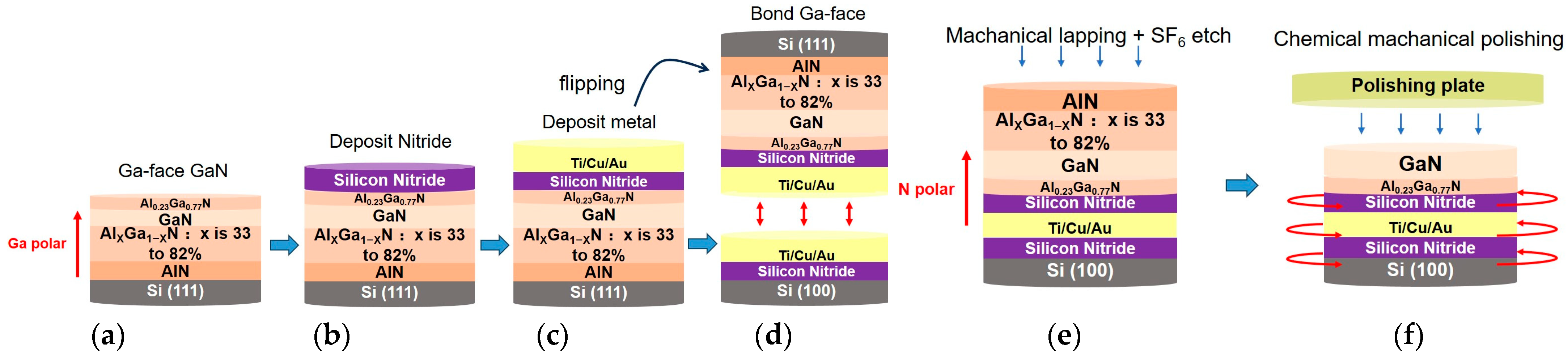
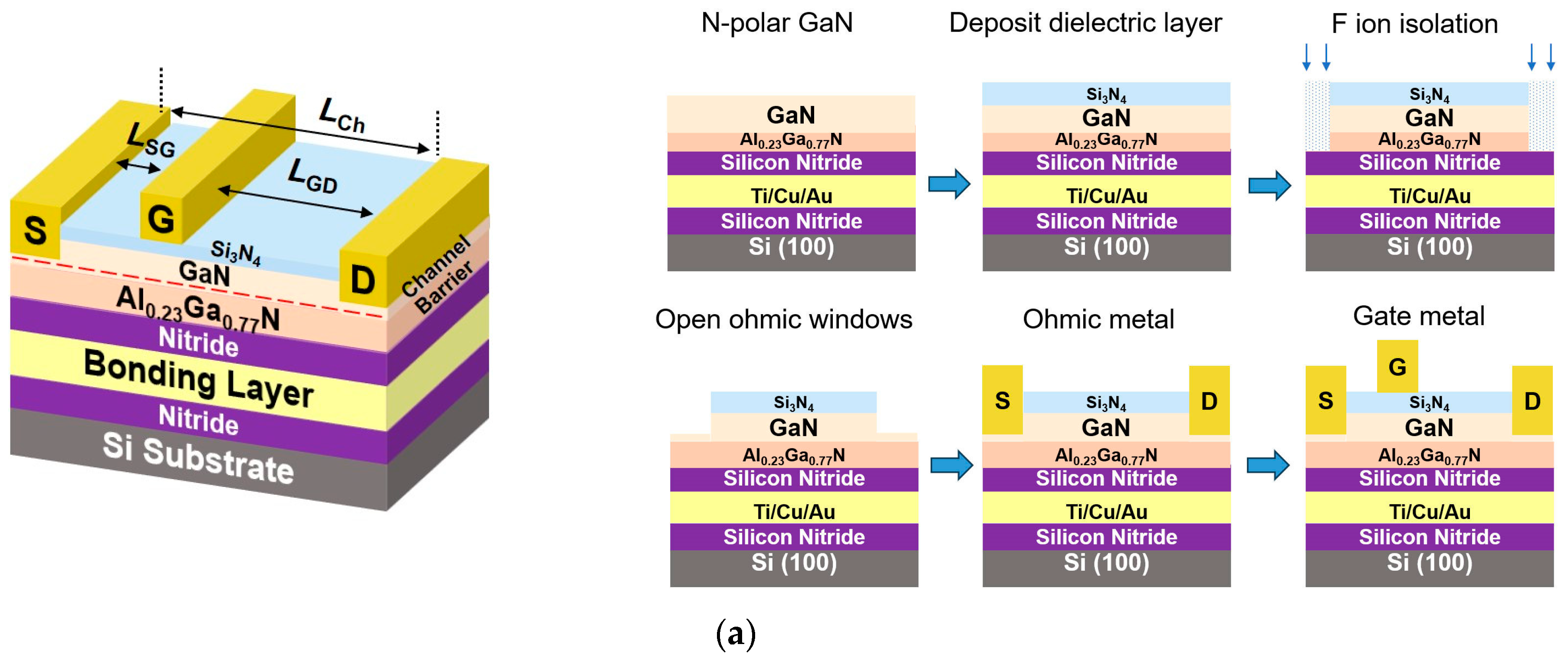
2. Experimental Methods

Figure 1 exhibits the main process flow of the proposed CMP-involved ELT technology for N-polar HEMT fabrication. The N-polar GaN structure was manufactured through the ELT method based on a high-quality Ga-polar AlGaN/GaN structure, which was epitaxially grown on a 6-inch Si (111) substrate using MOCVD. The Ga-polar device structure comprises a 23 nm Al0.23Ga0.77N barrier, a 300 nm GaN channel, a 1.5 µm GaN buffer, a 3.3 µm AlGaN buffer, and a 200 nm AlN nucleation layer, as shown in Figure 1a. The as-grown wafer exhibits a sheet resistance (Rsh) of 420.8 Ω/sq, a carrier density (ns) of 1.05 × 10¹³/cm2, and an electron mobility (µe) of 1420 cm2/V·s.
To be specific, the fabrication of the device commenced with the deposition of an Si3N4 diffusion buffer layer onto both the 6-inch Ga-polar AlGaN/GaN structure and the Si (100) substrate (Figure 1b), using low-pressure chemical vapor deposition (LPCVD). A Ti/Cu/Au (50 nm/800 nm/20 nm) stack was subsequently deposited onto both wafers by magnetron sputtering. Thereafter, Au–Au thermo-compressive wafer bonding was employed to bond the Ga-polar GaN wafer onto the Si (100) substrate (Figure 1c). Figure 1d shows the wafer bonding procedure for the Au–Au thermo-compressive wafer bonding of the Ga-polar GaN epiwafer onto the Si(100) carrier wafer. Following the removal of the Si (111) substrate by mechanical lapping and SF6-based dry etching, the N-polar AlN nucleation and AlxGa1−xN barrier were removed by CMP, as illustrated in Figure 1e,f. The specifics are covered in the following text. The schematic and process flow in Figure 2a depict the main manufacturing process of the N-Polar HEMT device, comprising dielectric deposition, F ion implantation for device isolation, ohmic contact fabrication, and gate fabrication, which will be discussed later. Figure 2b shows the FIB-SEM image of the fabricated N-polar HEMT; a clear Si3N4/metal bonding interlayer beneath the GaN/AlGaN heterojunction can be observed. Figure 2c demonstrates the successful bonding of the 6-inch epitaxial wafers with minor defects generated by particles affecting the subsequent substrate thinning process. After the wafer bonding, the original Si (111) substrate of the HEMT structure was thoroughly removed using mechanical lapping and SF6 plasma dry etching (Figure 1d). The wafer was then cut into 1.2 cm × 1.3 cm pieces and cleaned with an organic solvent.
After removal of the Si substrate, the exposed N-polar AlN nucleation layer was characterized using an atomic force microscope (AFM), showing a root-mean-square (RMS) surface roughness of 0.569 nm, as shown in Figure 3a. To expose the N-polar GaN surface, the AlN nucleation layer and AlGaN buffer layer needed to be removed via the CMP process conducted on a Single-Side Lapping Machine (AP-380, AM Technology Co., Ltd.). SiO2-KOH-based slurry with a pH of 9.7 was used to assist mechanical stress in polishing wafer surfaces. The stronger surface activity of N-polar GaN, due to its smaller Ga-N bond angle compared to Ga-polar GaN, renders it susceptible to an OH-ion attack [16]. The CMP process was divided into different steps, carried out continuously with varying carrier speeds to remove the AlN nucleation layer and AlxGa1−xN and GaN buffer layer due to the average etching rate of 600/400/50 nm/min in the weak alkaline solution.
The FIB-SEM results showed that the GaN channel thickness of the CMP sample was controlled to be 100 nm. A smooth N-polar GaN surface with a roughness as low as 0.216 nm was achieved, thanks to combined physical polishing with the chemical etching of CMP. As a comparison, another sample fabricated by ICP etching with Cl2/BCl3-based gas obtained an average etch rate of 320 nm/min was prepared in the meantime with a 100 nm thick N-polar GaN channel, referred to as the ICP sample. Due to the physical ion bombardment during dry etching [17], the GaN surface featured an increased roughness of 1.75 nm, as depicted in Figure 3c.
To assess the electrical properties of N-polar samples, MIS-HEMTs devices were fabricated on the CMP and ICP samples. Initially, a 20 nm PECVD-Si3N4 gate dielectric was deposited, and then the active regions of the devices were defined by F ion implantation, annealing for 5 min at 450 °C in an N2 ambient. After the Si3N4 window was opened for ohmic contact, the GaN channel was slightly etched down with Cl-based etching, and e-beam evaporation was used to form non-alloy ohmic contacts consisting of Ti/Au (25/200 nm); the Ni/Au (50/150 nm) stack was then evaporated as a gate metal. The MIS-HEMT featured a gate length of 3 µm, a gate-to-drain distance (LGD) of 15 µm, a gate-to-source distance (LGS) of 2.7 µm, and a width of 100 µm.

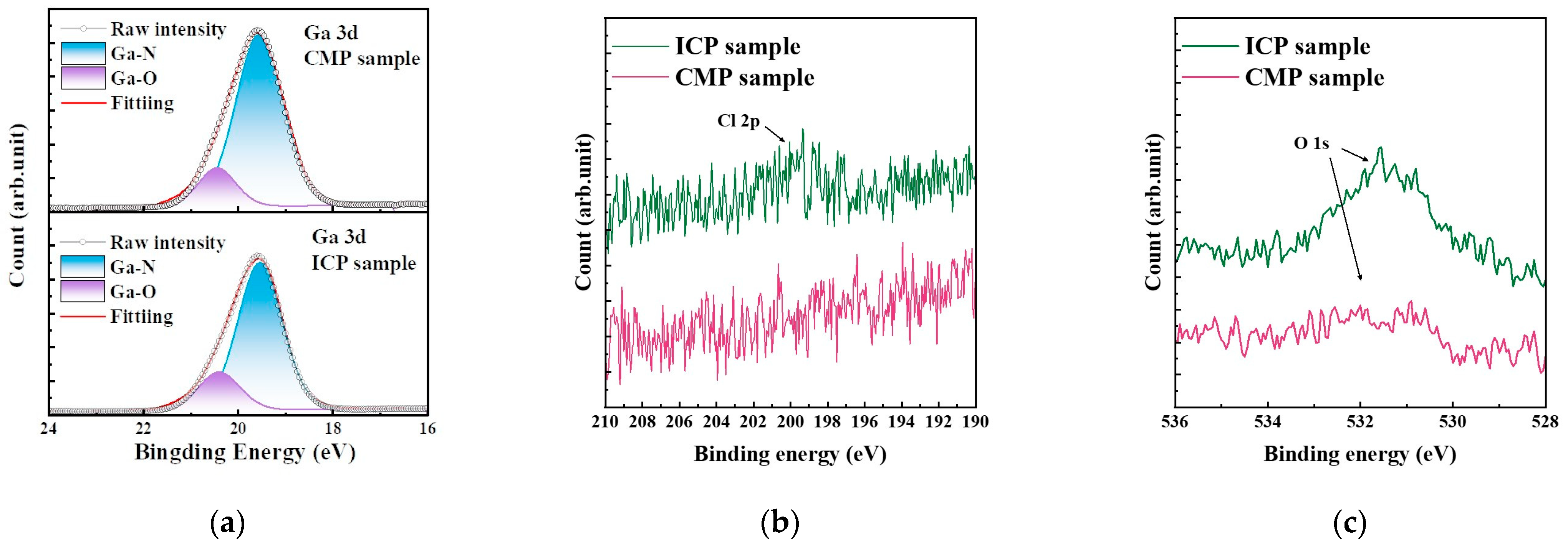
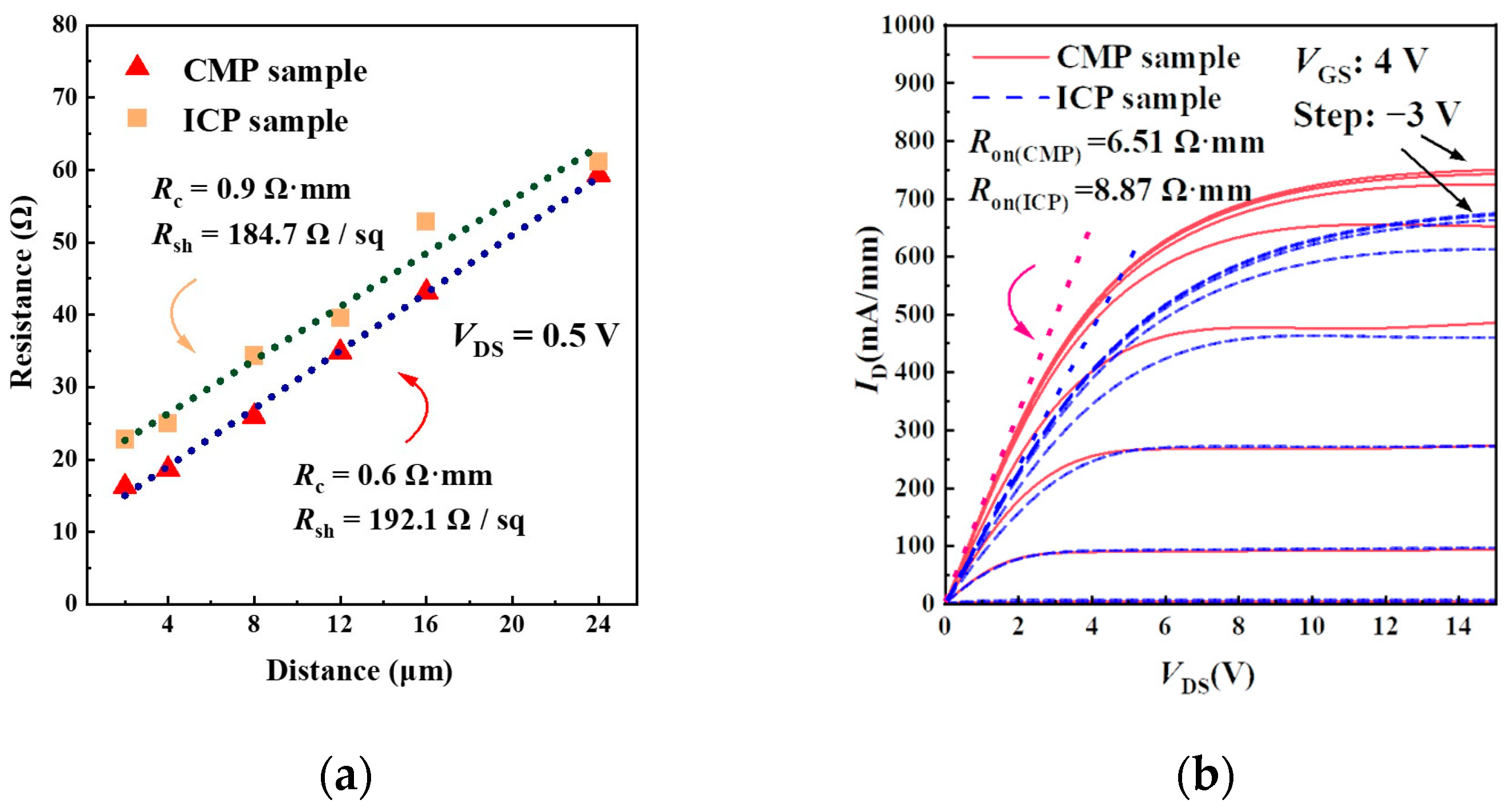
3. Results and Discussion

Different treatment methods for removing nucleation and buffer layers induced various impurity elements on the surface, and XPS was employed to investigate any stoichiometry modification on the N-polar GaN surface. With Gaussian fitting, the Ga 3d peak can be generally deconvoluted into two peaks contributing to Ga in GaN (Ga-(GaN) and Ga-(Ga2O3)), as shown in Figure 4a. Figure 4b,c shows the XPS energy spectrum of Cl 2p and O 1s core levels for CMP and ICP samples. As counted in Table 1, a significant Ga deficiency was evident after ICP treatment compared to the CMP sample, and the ICP sample had higher oxygen content (4.51%) and carbon content (15.6%) than those (1.27% and 8.09%) of the CMP sample, along with chlorine content (0.51%) on its surface. Byproducts like Al(Ga)Clx cannot be easily removed from the N-polar surface during ICP etching [18]. The presence of ion bombardment appears to degrade the electrical characteristics through ion-related chemical changes [19]. It should be noted that the results of XPS was element distribution at 1~2 nm beneath the GaN surface. However, this can be strong evidence to characterize the surface conditions of the N-polar GaN channel, considering its large thickness of 100 nm.
The electrical properties of the as-obtained N-polar HEMT after CMP are determined from Hall effect measurements using Van der Pauw structures, showing a sheet resistance (Rsh) of 244.7 Ω/sq, a mobility of 1230 cm2/V·s, and an ns of 2.24 × 1013 cm−2. After device fabrication, the CMP/ICP samples showed non-alloy contact resistances of 0.6/0.9 Ω mm, the Rsh of 192.1/184.7 Ω/sq, and the specific contact resistivity (ρc) of 2.14 × 10⁻⁵/4.86 × 10−5 Ω·cm2, as concluded in Figure 5a.
Figure 5b shows the output characteristics of the N-polar MIS-HEMTs fabricated via both CMP and ICP methods. The maximum current in the CMP sample is 756.1 mA/mm at VGS = 4 V, ~11% higher than that of the ICP sample (677.9 mA/mm). The on-resistance (RON) values of CMP and ICP sample are 6.51 Ω·mm and 8.87 Ω·mm, respectively. The improved output characteristics of the CMP sample are mainly due to the reduced deep-level states defects induced by energetic ion bombardment [15]. Notably, it was found that the output curves shown in Figure 5b show negligible self-heating effects, i.e., current drop at the operating conditions of high IDS = 756.1 mA/mm and high VDS = 15 V. The improved thermal dissipation abilities of our device can be attributed to the layers having the worst thermal conductivity, i.e., high-Al-content AlGaN buffers having been totally removed by the CMP/ICP etching process [20]. The remaining structures, i.e., GaN/AlGaN heterojunction, have relatively good thermal conductivity and stability. Figure 6a,b shows the capacitance–voltage (C-V) test structure and measurements of the CMP and ICP samples at 1 MHz. The total 2DEG sheet density, ns, can be obtained with the folowing formula [21]:
N C V = 2 q ε A 2 × d V d C 2
x = ε A C
A = π R 2
n s = + N C V x d x
where N C V is the concentration of electrons, q is the elementary charge, ε is the dielectric constant of the barrier layer, A is the Schottky junction area, C is the barrier capacitance under the anode bias V of Schottky barrier diode, x is the distance of the electrons from the GaN surface, and R is the radius of the anode. The results show that the total 2DEG sheet density of the CMP and ICP samples are 1.29 × 1013 cm−2 and 8.94 × 1012 cm−2 using Equations (1)–(4), which is the main reason for the higher maximum current of the CMP sample. A steeper rising slope at the first step shows better mutation and electron confinement in the CMP sample, and the slope at the second step is also observed to be steeper in the CMP sample, indicating that the Si3N4/GaN interface has a lower interface state density [22].
Figure 7a,b compares the transfer characteristics of the device on the CMP and ICP samples. Specifically, at VDS = 5 V and the same pinch-off voltage of −18 V, the CMP sample exhibited a transconductance of 61.1 mS/mm, surpassing that of the ICP sample (57.9 mS/mm). The CMP sample demonstrated an ION/IOFF ratio of 7.8 × 10⁴, with a subthreshold slope (SS) of 155 mV/dec, while the ICP sample exhibited an ION/IOFF ratio of 5.3 × 10⁴, with a SS of 233 mV/dec. This largely reduced SS value of the CMP sample further confirms the improved surface conditions of the N-polar GaN surface prepared via CMP methods [20].
Due to the Si3N4 gate dielectric, the gate leakage in both N-polar MIS-HEMTs was ~0.015 mA/mm at the pinch-off voltage, much lower than that in the previously reported Schottky N-polar HEMT (2–3 mA/mm) [14]. Further reduction in leakage could be achieved by optimizing the gate leakage through LPCVD growth of the Si3N4 gate dielectric [23]. In addition, the CMP sample in Figure 7c shows a large gate breakdown voltage of 23 V, corresponding to an ultra-high gate swing of ~40 V. In comparison, the gate breakdown of the ICP sample was premature at 18 V, mainly due to the inferior surface conditions caused by dry etching. These results verify the compatibility between the N-polar GaN surface obtained from CMP-incorporated layer transfering technology and PECVD Si3N4 for high-performance N-polar GaN HEMT application. It should be noted that the AlGaN back barrier employed in this work is based on a well-developed Ga-polar GaN-on-Si epitaxial structure. It is of great interest and significance to further investigate the influences of Al% of the AlGaN back barrier on the electrical characteristics of N-polar GaN MIS-HEMTs to further propel the development of such device technologies towards high-efficiency power electronic devices.

4. Conclusions

A method to obtain an N-polar GaN surface via CMP-involved ELT achieving low surface roughness (RMS = 0.216 nm) and low-induced impurity-like elements like Cl, C, and O has ben presented in this article. The electronic properties show a sheet resistance (Rsh) of 244.7 Ω/sq, a mobility of 1230 cm2/V·s, and an ns of 2.24 × 1013 cm−2. Compared to the ICP approach, CMP can avoid damage from ion bombardment and provide improved surface conditions, resulting in a better performance of the fabricated N-polar GaN/AlGaN MIS-HEMTs, with 756.1 mA/mm maximum current, 0.015 mA/mm (@VGS = −30 V) gate leakage, and reduced subthreshold slope. This approach highlights the feasibility of CMP-involved ELT and offers a viable route of fabricating high-performance N-polar devices.

Author Contributions

Conceptualization, B.G. and L.Z.; Methodology, B.G., L.Z., J.Z., Z.W. and A.Y.; Software, B.G., L.Z., J.Z. and R.X.; Validation, B.G. and G.Y.; Formal analysis, B.G., G.Y., L.Z., J.Z., Z.W. and A.Y.; Investigation, B.G., L.Z., R.X., Y.L., B.L., X.Z., Z.D. and X.D.; Resources, G.Y. and B.Z.; Data curation, X.Z.; Writing—original draft, B.G.; Writing—review and editing, L.Z., J.Z., Z.W. and B.Z.; Supervision, Z.Z. and B.Z.; Project administration, Z.Z. and B.Z.; Funding acquisition, G.Y., Z.Z. and B.Z. All authors have read and agreed to the published version of the manuscript.

Funding

This work was supported by the Youth Innovation Promotion Association of the Chinese Academy of Sciences (Grant No. 2020321), National Natural Science Foundation of China (Grant No. 92163204), the Key Research and Development Program of Jiangsu Province (Grant No. BE2022057-1), and the Students’ Innovation and Entrepreneurship Foundation of USTC (CY2023X001). The authors would like to thank the Nano Fabrication Facility, Platform for Characterization and Test, Vacuum Interconnected Nanotech Workstation (NANO-X), and Suzhou Institute of Nano-Tech and Nano-Bionics, Chinese Academy of Sciences.

Data Availability Statement

The original contributions presented in the study are included in the article, further inquiries can be directed to the corresponding authors.

Conflicts of Interest

Author Zhongkai Du was employed by the company Suzhou Powerhouse Electronics Technology Co., Ltd. The remaining authors declare that the research was conducted in the absence of any commercial or financial relationships that could be construed as a potential conflict of interest.

References

  1. Zhang, W.; Zhang, J.; Xiao, M.; Zhang, L.; Hao, Y. Al0.3Ga0.7N/GaN (10 nm)/Al0.1Ga0.9N HEMTs with low leakage current and high three-terminal breakdown voltage. IEEE Electron Device Lett. 2018, 39, 1370–1372. [Google Scholar] [CrossRef]
  2. Zhang, H.; Huang, C.; Song, K.; Yu, H.; Xing, C.; Wang, D.; Liu, Z.; Sun, H. Compositionally graded III-nitride alloys: Building blocks for efficient ultraviolet optoelectronics and power electronics. Rep. Prog. Phys. 2021, 84, 044401. [Google Scholar] [CrossRef]
  3. Du, H.; Liu, Z.; Hao, L.; Xing, W.; Zhou, H.; Zhao, S.; Zhang, J.; Hao, Y. High-Performance AlN/GaN MISHEMTs on Si With in-situ SiN Enhanced Ohmic Contacts for Mobile mm-Wave Front-End Applications. IEEE Electron Device Lett. 2023, 44, 911–914. [Google Scholar] [CrossRef]
  4. Masui, H.; Keller, S.; Fellows, N.; Fichtenbaum, N.A.; Furukawa, M.; Nakamura, S.; Mishra, U.K.; DenBaars, S.P. Luminescence characteristics of N-polar GaN and InGaN films grown by metal organic chemical vapor deposition. Jpn J. Appl. Phys. 2009, 48, 071003. [Google Scholar] [CrossRef]
  5. Li, W.; Romanczyk, B.; Akso, E.; Guidry, M.; Hatui, N.; Wurm, C.; Liu, W.; Shrestha, P.; Collins, H.; Clymore, C.; et al. Record 94 GHz performance from N-polar GaN-on-sapphire MIS-HEMTs: 5.8 W/mm and 38.5% PAE. In Proceedings of the 2022 International Electron Devices Meeting (IEDM), San Francisco, CA, USA, 3–7 December 2022; pp. 11–12. [Google Scholar]
  6. Wong, M.H.; Keller, S.; Nidhi, S.D.; Denninghoff, D.J.; Kolluri, S.; Brown, D.F.; Lu, J.; Fichtenbaum, N.A.; Ahmadi, E.; Singisetti, U.; et al. N-polar GaN epitaxy and high electron mobility transistors. Semicond. Sci. Technol. 2013, 28, 074009. [Google Scholar] [CrossRef]
  7. Wong, M.H.; Pei, Y.; Palacios, T.; Shen, L.; Chakraborty, A.; McCarthy, L.S.; Keller, S.; DenBaars, S.P.; Speck, J.S.; Mishra, U.K. Low nonalloyed Ohmic contact resistance to nitride high electron mobility transistors using N-face growth. Appl. Phys. Lett. 2007, 91, 232103. [Google Scholar] [CrossRef]
  8. Wang, Y.L.; Ren, F.; Zhang, U.; Sun, Q.; Yerino, C.D.; Ko, T.S.; Cho, Y.S.; Lee, I.H.; Han, J.; Pearton, S.J. Improved hydrogen detection sensitivity in N-polar GaN Schottky diodes. Appl. Phys. Lett. 2009, 94, 212108. [Google Scholar] [CrossRef]
  9. Keller, S.; Fichtenbaum, N.; Wu, F.; Lee, G.; DenBaars, S.P.; Speck, J.S.; Mishra, U.K. Effect of the nucleation conditions on the polarity of AlN and GaN films grown on C-face 6H–SiC. Jpn. J. Appl. Phys. 2006, 45, L322. [Google Scholar] [CrossRef]
  10. Sumiya, M.; Yoshimura, K.; Ito, T.; Ohtsuka, K.; Fuke, S.; Mizuno, K.; Yoshimoto, M.; Koinuma, H.; Ohtomo, A.; Kawasaki, M. Growth mode and surface morphology of a GaN film deposited along the N-face polar direction on c-plane sapphire substrate. J. Appl. Phys. 2000, 88, 1158–1165. [Google Scholar] [CrossRef]
  11. Storm, D.F.; Katzer, D.S.; Meyer, D.J.; Binari, S.C. Oxygen incorporation in homoepitaxial N-polar GaN grown by radio frequency-plasma assisted molecular beam epitaxy: Mitigation and modeling. J. Appl. Phys. 2012, 112, 013507. [Google Scholar] [CrossRef]
  12. Sumiya, M.; Yoshimura, K.; Ohtsuka, K.; Fuke, S. Dependence of impurity incorporation on the polar direction of GaN film growth. Appl. Phys. Lett. 2000, 76, 2098–2100. [Google Scholar] [CrossRef]
  13. Chung, J.W.; Piner, E.L.; Palacios, T. N-face GaN/AlGaN HEMTs fabricated through layer transfer technology. IEEE Electron Device Lett. 2008, 30, 113–116. [Google Scholar] [CrossRef]
  14. Ryu, K.K.; Roberts, J.C.; Piner, E.L.; Palacios, T. Thin-body N-face GaN transistor fabricated by direct wafer bonding. IEEE Electron Device Lett. 2011, 32, 895–897. [Google Scholar] [CrossRef]
  15. Yu, Z.; Zhang, L.; Yu, G.; Deng, X.; Jiang, C.; Tang, W.; Yin, H.; Liu, W.; Chen, Z.; Zhang, B. High quality of N-polar GaN film fabricated by layer transfer technology using high selective material removal rate of CMP. Mat. Sci. Semicon. Proc. 2022, 141, 106440. [Google Scholar] [CrossRef]
  16. Tautz, M.; Weimar, A.; Graßl, C.; Welzel, M.; Díaz Díaz, D. Anisotropy and Mechanistic Elucidation of Wet-Chemical Gallium Nitride Etching at the Atomic Level. Phys. Status Solidi A 2020, 217, 2000221. [Google Scholar] [CrossRef]
  17. Fang, C.Y.; Huang, W.J.; Chang, E.Y.; Lin, C.F.; Feng, M.S. Etching damages on AlGaN, GaN and InGaN caused by hybrid inductively coupled plasma etch and photoenhanced chemical wet etch by Schottky contact characterizations. Jpn. J. Appl. Phys. 2003, 42, 4207. [Google Scholar] [CrossRef]
  18. Ge, X.; Yin, X.; Zeng, Q.; Feng, Q.; Wang, X.; Li, Q.; Li, C. Study of dry etched N-polar (Al) GaN surfaces obtained by inductively coupled plasma etching. Front. Phys. 2022, 10, 1042998. [Google Scholar] [CrossRef]
  19. Cheung, R.; Rong, B.; van der Drift, E.W.J.M.; Sloof, W.G. Etch mechanism and etch-induced effects in the inductively coupled plasma etching of GaN. J. Vac. Sci. Technol. B 2003, 21, 1268–1272. [Google Scholar] [CrossRef]
  20. Zhang, H.; Sun, Y.; Hu, K.; Yang, L.; Liang, K.; Xing, Z.; Wang, H.; Zhang, M.; Yu, H.; Fang, S.; et al. Boosted high-temperature electrical characteristics of AlGaN/GaN HEMTs with rationally designed compositionally graded AlGaN back barriers. Sci. China Inf. Sci. 2023, 66, 182405. [Google Scholar] [CrossRef]
  21. Liu, S.; Zhang, J.; Zhao, S.; Shu, L.; Song, X.; Wang, C.; Li, T.; Liu, Z.; Hao, Y. Characterization of trap states in AlN/GaN superlattice channel high electron mobility transistors under total-ionizing-dose with 60Co γ-irradiation. Appl. Phys. Lett. 2022, 120, 202102. [Google Scholar] [CrossRef]
  22. Mizue, C.; Hori, Y.; Miczek, M.; Hashizume, T. Capacitance–voltage characteristics of Al2O3/AlGaN/GaN structures and state density distribution at Al2O3/AlGaN interface. Jpn. J. Appl. Phys. 2011, 50, 021001. [Google Scholar] [CrossRef]
  23. Zhang, Z.; Fu, K.; Deng, X.; Zhang, X.; Fan, Y.; Sun, S.; Song, L.; Xing, Z.; Huang, W.; Yu, G.; et al. Normally off AlGaN/GaN MIS-high-electron mobility transistors fabricated by using low pressure chemical vapor deposition Si3N4 gate dielectric and standard fluorine ion implantation. IEEE Electron Device Lett. 2015, 36, 1128–1131. [Google Scholar] [CrossRef]
Figure 1. Main process flow of layer transfer technology to fabricate N-polar GaN. (a) Epitaxial Growth (b) Deposition of Nitride (c) Deposition of Metal (d) Bonding Ga-face (e) Mechanical Lapping and SF6 Etching (f) Chemical Mechanical Polishing (CMP).
Crystals 14 00253 g001
Figure 2. (a) Schematic and fabrication process of the N-polar MIS-HEMT device with Si3N4 gate dielectric, GaN channel layer, Al0.23Ga0.77N barrier layer, silicon nitride diffusion buffer layer, and metal bonding layer. (b) Focused ion beam scanning electron microscopy (FIB-SEM) cross-section image of N-polar MIS-HEMT device. (c) Ultrasound scanning microscope (USM) image of 6-inch epitaxial wafer after metal bonding.
Crystals 14 00253 g002aCrystals 14 00253 g002b
Figure 3. AFM image of (a) N-polar AlN surface after Si substrate removal (RMS = 0.569 nm). (b) N-polar GaN surface exposed by CMP (RMS = 0.216 nm). (c) N-polar GaN exposed by ICP etching (RMS = 1.75 nm).
Crystals 14 00253 g003
Figure 4. XPS core-level spectrum of (a) Ga 3d, (b) Cl 2p and (c) O 1s for the CMP and ICP samples.
Crystals 14 00253 g004
Figure 5. Comparison of (a) transfer line method (TLM) and (b) output characteristics for CMP- and ICP-based MIS-HEMTs.
Crystals 14 00253 g005
Figure 6. (a) C−V test structure and (b) C−V characteristics of CMP and ICP samples at 1 MHz.
Crystals 14 00253 g006
Figure 7. Comparison of (a) transfer characteristics, (b) transfer characteristics in logarithmic coordinates, and (c) gate breakdown characteristics for CMP- and ICP-based MIS-HEMTs.
Crystals 14 00253 g007
Table 1. Surface elemental composition of the ICP and CMP samples extracted via XPS.
SampleSurface Elemental Composition (at. %)
GaNOCCl
ICP36.4642.924.5115.60.51
CMP39.7250.921.278.09-
Disclaimer/Publisher’s Note: The statements, opinions and data contained in all publications are solely those of the individual author(s) and contributor(s) and not of MDPI and/or the editor(s). MDPI and/or the editor(s) disclaim responsibility for any injury to people or property resulting from any ideas, methods, instructions or products referred to in the content.

