Article

The Effect of Sputtering Target Density on the Crystal and Electronic Structure of Epitaxial BaTiO3 Thin Films

1
School of Material Science and Chemical Engineering, Ningbo University, Ningbo 315211, China
2
Ningbo Institute of Materials Technology and Engineering, Chinese Academy of Sciences, Ningbo 315201, China
3
School of Materials Science and Engineering, Xiangtan University, Xiangtan 315201, China
4
Center of Materials Science and Optoelectronics Engineering, University of Chinese Academy of Sciences, Beijing 100049, China
*
Authors to whom correspondence should be addressed.
These authors contributed equally to this work.
Crystals 2024, 14(4), 304; https://doi.org/10.3390/cryst14040304
Submission received: 20 February 2024 / Revised: 7 March 2024 / Accepted: 12 March 2024 / Published: 26 March 2024
(This article belongs to the Special Issue Epitaxial Growth and Application of Metallic Oxide Thin Films)

Abstract

:
Barium titanate (BaTiO3) is a promising material for silicon-integrated photonics due to its large electro-optical coefficients, low loss, high refractive index, and fast response speed. Several deposition methods have been employed to synthesize BaTiO3 films. Magnetron sputtering is one of these methods, which offers specific advantages for growing large-scale films. However, there is a scarcity of studies investigating the effect of sputtering target density on the quality of BaTiO3 films. Therefore, this study aims to uncover the effect of sputtering targets on the crystal and electronic structures of epitaxial BaTiO3 thin films. Two BaTiO3 ceramic targets were sintered at different densities by altering the sintering temperatures. The crystal structure and chemical composition of the targets were then characterized using X-ray diffraction, Raman spectroscopy, and scanning electron microscopy with energy-dispersive X-ray spectroscopy. Subsequently, BaTiO3 epitaxial films were grown by magnetron sputtering using these two targets. The crystal and electronic structures of the BaTiO3 films were analyzed using high-resolution X-ray diffraction, X-ray photoemission spectroscopy, atomic force microscopy, and spectroscopic ellipsometry. Notably, the BaTiO3 films grown with high-density targets show superior quality but contain oxygen vacancies, whereas those films synthesized with low-density targets display high surface roughness. These findings provide insights into the effect of sputtering target density on the crystal and electronic structures of epitaxial BaTiO3 thin films.

1. Introduction

Ferroelectric materials with the ABO3 perovskite structure can exhibit optical anisotropy due to the breaking of central inversion symmetry [1,2,3,4]. The alteration of its refractive index in response to the applied electric field is known as the electro-optical effect, e.g., the Pockels effect [5,6]. BaTiO3 (BTO), the first discovered perovskite ferroelectric, undergoes a tetragonal-cubic phase transition at 120 °C. In the tetragonal phase at room temperature, Ti ions deviate from the central position of the oxygen octahedron, contributing to a significant r33 value [7]. Typically, the Pockels coefficients for bulk BTO crystals (r42 ~1300 pm/V) is an order of magnitude higher than for lithium niobate (LNO) crystals (r42 ~32 pm/V), which have long served as the industry standard for electro-optic devices [8,9,10]. Moreover, compared to the intricate bonding process of LNO, BTO can be directly deposited on the Si substrates with the STO buffer layer [11,12,13]. Furthermore, BTO possesses desirable characteristics such as low loss, high refractive index, and fast response speed, making it a promising material for photonics applications and garnering significant attention [14,15,16]. However, bulk BTO crystals are prone to developing cracks during the phase change process due to stress concentration, and the presence of ferroelectric domain walls reduces transmittance through refraction and reflection of light. Therefore, the development of highly oriented BTO films with exceptional crystal quality is a crucial technological advancement.
Currently, high-quality BTO is primarily grown using metal-organic vapor deposition (MOCVD) [17], molecular beam epitaxy (MBE) [18,19], pulsed laser deposition (PLD) [14,20], and magnetron sputtering [21,22]. In 2018, Stefan Abel et al. conducted groundbreaking research by integrating BTO into Si using MBE and extracted a Pockels coefficient of r42 ~923 pm/V [23]. The Landau–Devonshire theory confirms the dependence of the electro-optical effect on the thickness of optical films, highlighting the necessity for films to reach a critical relaxation thickness [24,25]. However, MBE has a slow growth rate and is susceptible to flux drift during prolonged operation, resulting in non-stoichiometric films, which can significantly affect its optical properties. Ti-rich BTO films exhibit columnar growth [26], while Ba-rich films tend to form RP phase boundaries and have high surface roughness [27], which increases defect density and reduces the crystal quality of the film. Thus, MBE is not suitable for growing thick films. Although PLD enables rapid growth with high-quality results, it is challenging to apply in large-scale industrial deposition due to limitations in plasma plume volume. As a similarly high-energy growth method, magnetron sputtering technology is widely used in industry due to its affordability, large growth size, and high uniformity. However, the crystal quality of BTO thin films grown using magnetron sputtering is not as good as those grown using PLD [28] and MBE [29]. Therefore, further exploration of the magnetron sputtering growth process is necessary.
During the growth of transparent conductive oxide films, it has been revealed that the selection of targets can significantly influence the optical properties of the films [30,31,32,33,34]. Additionally, arc discharge induced by target conditions has been a common phenomenon for sputtering cathodes, particularly in reactive sputtering [35]. Addressing arc discharge damage to targets and films has been challenging for a long time. During sputtering, the kinetic energy of high-energy particles bombarding the target is mainly converted into heat energy. Previous studies have indicated that at a power density of 5 W/cm2, the surface temperature of a metal target can exceed 700 °C [36]. Moreover, the dielectric properties of ceramic targets can amplify their thermal effects compared to metals. The density of the target material impacts surface thermal conductivity, leading to thermal stress concentration around internal defects. Insufficient cooling can result in target material cracking, reducing the target’s lifespan and affecting deposition process repeatability [31]. Furthermore, variable sputtering rates at grains, grain boundaries, and holes generate nodules on the surface, leading to irregular morphology [32]. In plasmas, most of the voltage drop occurs within a very thin sheath on the target surface. At locations with a large curvature of the target surface, due to the geometric enhancement effect, the local charge density is high, which can easily cause arc discharge and lead to unstable deposition. Consequently, understanding the impact of targets during the sputtering process on BTO films has emerged as an attractive research topic.
In this paper, we employ the traditional solid-state sintering method to prepare two barium titanate ceramic targets with different densities. These targets are then used for film growth using a homemade high-pressure magnetron sputtering epitaxy system. We systematically investigate the effects of target density on the quality of the films.

2. Experimental Procedure

Two targets with different densities were prepared using traditional solid-state sintering methods at varying sintering temperatures. The TiO2 (99.99% purity) and BaCO3 (99.99% purity) powders were mixed in a molar ratio of 1:1 and calcined in a muffle furnace at 1000 °C for 2 h. Subsequently, the resulting reaction products were ball-milled and pressed into a 5 mm thick and 2-inch diameter ceramic blank. Finally, the two targets were sintered at temperatures of 1200 °C and 1350 °C, which we denote as “1200 target” and “1350 target”, respectively. After sintering, we measured the dimensions and mass of the targets, and their relative densities were calculated to be 82% and 93%, respectively.
We used a homemade off-axis RF high-pressure magnetron sputtering system to epitaxially deposit BTO films on STO (001) single-crystal substrates [37]. The distance from the center of the target of our equipment to the center of the sample stage is 150.5 mm. Before film growth, the vacuum chamber was evacuated to a base pressure of 3.0 × 10⁻⁷ Torr, and the BTO target surfaces were pre-sputtered for 30 min to remove contaminants. The RF power was set to 60 W, and the substrate temperature was maintained at 850 °C during the film growth. Sputtering was performed using high-purity argon as the process gas, while the total pressure was maintained at 15 mTorr. However, the airflow rates of the 1200 target and the 1350 target were ~3.0 sccm and ~4.0 sccm, respectively, indicating inconsistent gas output from the targets during the sputtering process. The film deposited over six hours had a thickness of 67 nm, and the growth rates of the two targets were similar, at approximately 11 nm/h. We denote the films deposited using the 1200 °C-sintered target as “1200 film” and those from the 1350 °C-sintered target as “1350 film”.
The phase and crystal structures of the targets were analyzed using a D8 Advance X-ray polycrystalline powder diffractometer (XRD) (Bruker, Karlsruhe, Germany) and a inVia Reflex confocal Raman spectroscopy (Raman) (Renishaw, Gloucester, UK). The surface morphology of the targets was investigated using an EVO 08 scanning electron microscope (SEM) (ZEISS, Jena, Germany), and the element distribution in the micro area was analyzed using its equipped energy spectrometer (EDS). The structure of the films was characterized using a D8 Discovery high-resolution single-crystal diffractometer (HR-XRD) (Bruker, Karlsruhe, Germany) equipped with a monochromatic Cu Kα X-ray source (wavelength of 1.5406 Å, tube voltage of 40 kV). The surface components of the film were detected using an AXIS SUPRA X-ray photoelectron spectrometer (XPS) (Kratos, Manchester, UK) equipped with Monochromatic Al Kα radiation (1486.74 eV). During the XPS process, an electron flood gun was utilized to eliminate charging effects. The samples were corrected for the equipment’s work function. The surface morphology and roughness of the films were analyzed using a Dimension Icon atomic force microscope (AFM) (Bruker, Karlsruhe, Germany). M-2000DI Spectroscopic ellipsometry (SE) (J. A. Woollam, Lincoln, NE, USA) was performed to characterize the optical properties of the films, with wavelengths ranging from 400 nm to 1600 nm [38].

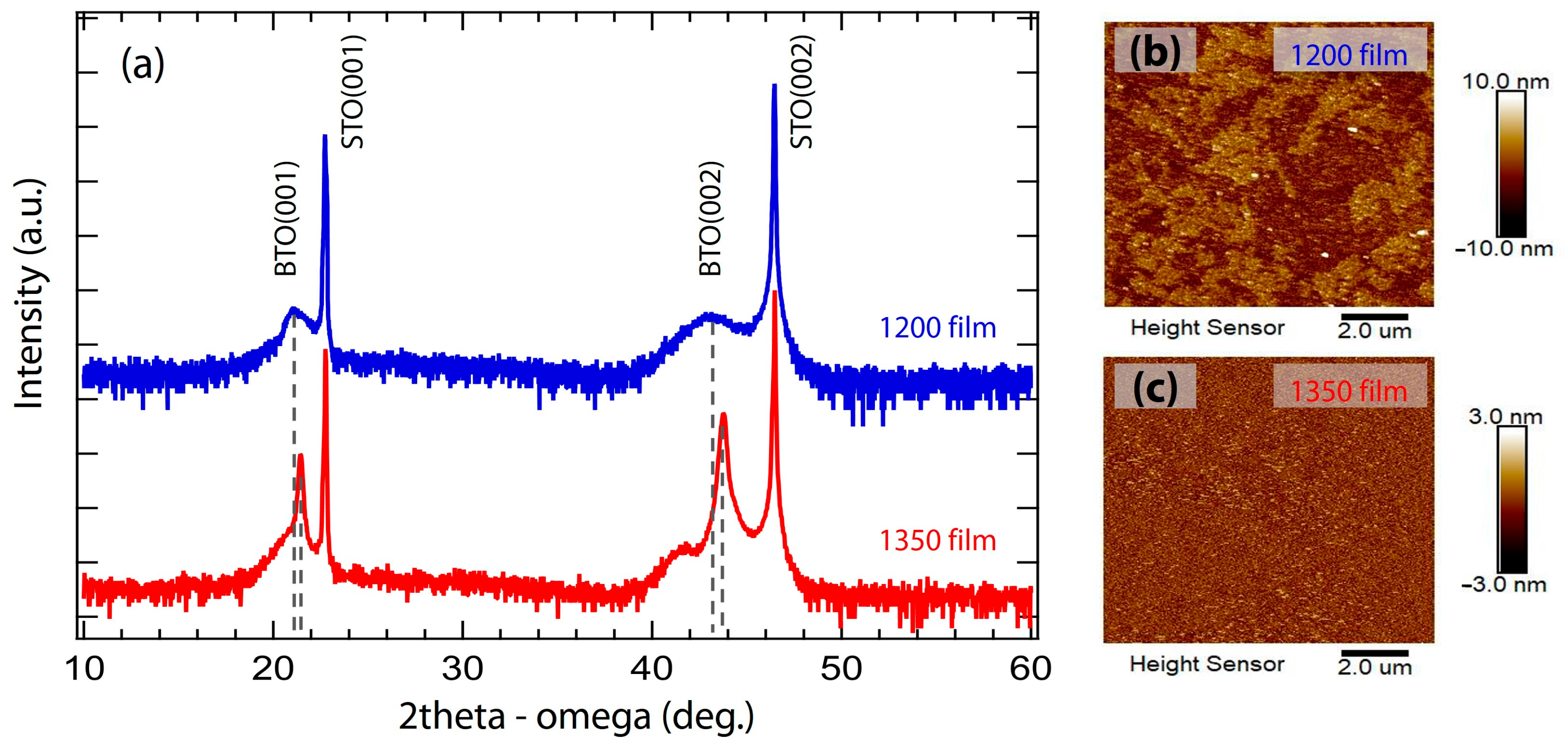
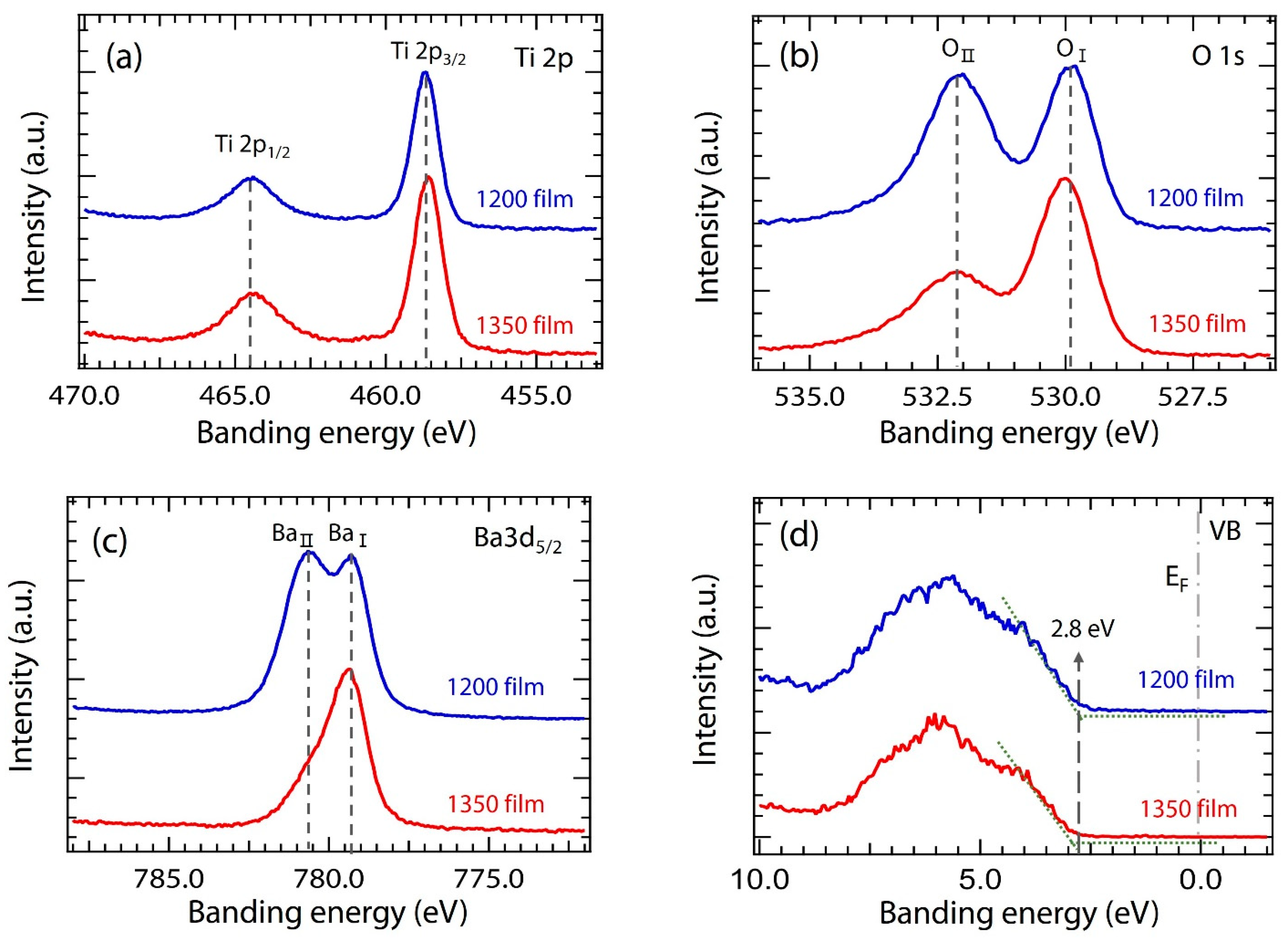
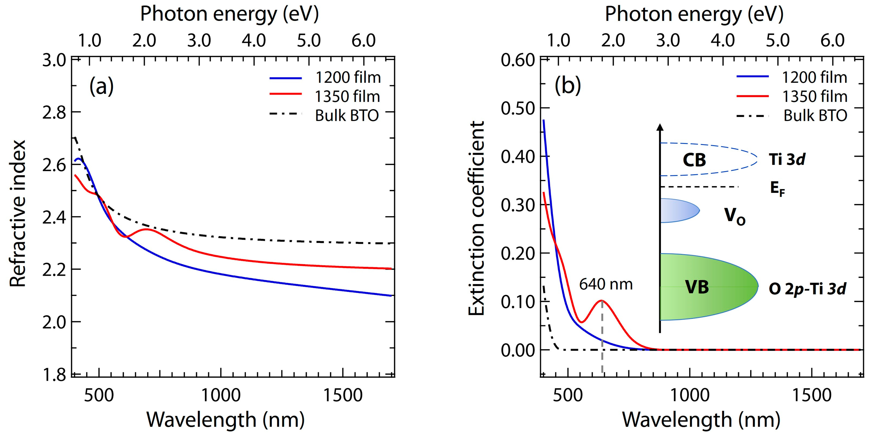
3. Results and Discussion

Figure 1a illustrates the XRD θ–2θ scans of BTO ceramic targets sintered at different temperatures: 1200 °C (blue solid line) and 1350 °C (red solid line). The diffraction peaks of the samples can be compared with the standard BTO PDF card (05-0626) [39], confirming that they can be indexed to a single tetragonal perovskite structure with a space group of P3mm. No impurity phase is present in either BTO target. Notably, all diffraction peaks exhibit a splitting phenomenon [40]. Specifically, the 002/200 diffraction peak is commonly used to identify ferroelectric BTO with a tetragonal structure [41].
Figure 1b presents the Raman spectrum. In the perfect cubic (Pm3m) space point group, four optical phonons exist, namely, triple degenerate F1u and non-degenerate F2u modes. Neither F1u nor F2u exhibits Raman activity, with only F2u showing infrared activity. Therefore, the ideal cubic paraelectric phase should not exhibit any Raman signal. In the tetragonal ferroelectric phase (P4mm), F1u splits into doubly degenerate E and non-degenerate A1 modes, while F2u splits into B1 and E modes [42]. Additionally, each optical phonon branch splits into transverse (TO) and longitudinal (LO) modes due to the presence of long-range electrostatic forces in the ferroelectric phase. The expression 3[A1(TO) + A1(LO)] + B1 + 4[E(TO) + E(LO)] represents all phonon branches in the tetragonal phase of BTO [43]. During the tetragonal-cubic phase transition process, certain characteristic peaks of ferroelectric BTO, such as A1(LO1) ~170 cm−1, B1/E(TO2) ~305 cm−1, A1(LO2) ~473 cm−1, and A1(TO3)/E(LO) ~715 cm−1, abruptly disappear when T > Tc [44]. On the other hand, A1(TO2) ~263 cm−1 and A1(TO3) ~515 cm−1 persist in the cubic paraelectric phase. From Figure 1b, it is evident that both the 1200 target and 1350 target exhibit characteristic peaks of the tetragonal ferroelectric phase and no significant difference in peak positions and intensities. This further substantiates the minimal impact of different sintering temperatures on the crystal structure of the targets.
To investigate the micromorphology and element distribution of the as-synthesized BTO ceramic targets, scanning electron microscopy (SEM) and energy-dispersive X-ray spectroscopy (EDS) mapping were conducted. Figure 2a displays the BTO ceramics sintered at 1200 °C, which consists of round-shaped particles with a narrow size distribution and numerous interconnected three-dimensional holes. The average particle size of the 1200 target was determined to be approximately 0.5 μm, and the grain distribution appears to be dispersed. There are many dangling bonds around holes and at grain boundaries, and the nucleation energy of atoms is low. Sputtering erodes along the pores, and fragments can easily dissociate from the matrix. Under high-temperature conditions, these particles form nodules on the target surface, increasing the arc discharge density [45]. In contrast, with increasing sintering temperature, the 1350 target exhibits the production of a significant amount of liquid phase as shown in Figure 2d. This promotes bonding between grains, resulting in a denser structure without noticeable microscopic holes. EDS mapping of Ti Kα1 and Ba Lα1 (Figure 2b,c, respectively) for the 1200 target reveals a uniform distribution of Ti and Ba elements. Similarly, Figure 2e,f for the 1350 target demonstrate consistent results in terms of element distribution.
Figure 3a displays 2θ-ω scans of films grown through off-axis magnetron sputtering using two targets with different densities. Both films exhibit a highly textured character along the (00l) reflections without any secondary phase. Comparing the 1350 film (FWHM ~0.6°) with the 1200 film, it is evident that the diffraction peak of the latter (FWHM ~2°) is wider, indicating poorer crystal quality. The micropores in the 1200 target cause a reduction in the thermal conductivity and mechanical properties of the target. Deposition instability leads to reduced crystal quality. The dominant feature of BTO films lies in the (002) diffraction peaks around 42.96° (1250 film) and 43.74° (1300 film). Furthermore, the out-of-plane lattice constant of the film was determined through the (002) plane, resulting in c = 4.210Å for 1200 film and c = 4.139 Å for 1350 film. Both values are larger than the bulk BTO value of c = 4.036 Å. Notably, the 1350 film exhibited an additional low-angle diffraction peak with a lattice constant of c = 4.324 Å, indicating a tetragonality increase of up to 7.1%, surpassing the expected 5.8% expansion of the c-axis due to the coherently strained thermal mismatch between BTO and STO. This deviation is believed to be caused by lower oxygen partial pressure during the growth of 1350 film, resulting in the formation of oxygen vacancies [26]. Conversely, the microscopic pores in the 1200 target released air into the chamber during film deposition, increasing the oxygen partial pressure. This phenomenon aligns with a similar lattice-expansion effect observed in low oxygen pressure deposition by PLD, where oxygen vacancy defect dipoles are formed and act as point defects to promote substrate strain relaxation [46]. Ultimately, the coupling effect of substrate strain and oxygen vacancies in the early growth stages leads to the low-angle diffraction peak, while substrate strain relaxation upon reaching the critical thickness accounts for the high-angle diffraction peak.
Figure 3b,c present the surface morphology and roughness of epitaxial BTO films, with a scanning area of 10 × 10 μm2, as measured by AFM. It can be observed that the roughness of the 1200 film (RMS = 2.01 nm) is higher than that of the 1350 film (RMS = 0.52 nm), aligning with the reported trend where roughness increases with oxygen pressure [47]. This finding further supports the notion that the density of the target material impacts the oxygen partial pressure during the growth process.
Figure 4a shows the Ti 2p spectra of the 1200 film and 1350 film. The Ti 2p spectrum consists of the 2p3/2 and 2p1/2 spin–orbital components and is found to be symmetric, indicating a well-defined single electronic state for Ti atoms in TiO6 octahedra. The position of the Ti 2p peak in both films is consistent, and no Ti3+ components were found.
The O 1s spectra of the samples are displayed in Figure 4b. The main peak, denoted as O I, is located at a lower binding energy (529.8 eV) and is attributed to the oxygen in the lattice position. The peak situated +2.3 eV above the main peak is labeled as O II (532 eV). Typically, on the surface of the perovskite oxide film, there exist adsorption products such as hydroxide (~531 eV), carbonate (~532 eV), peroxide (~532 eV), and molecular water (~533 eV) [48]. These result in a high binding energy peak of O 1s. Although the peak position of CO32− is around 532 eV, no conspicuous signal of CO32− appears in the C 1s spectra. Hence, based on the comparison of peak positions, we assign O II to the peroxide.
Figure 4c displays the Ba 3d5/2 spectra. The peak at the lower binding energy is labeled as Ba I (779.3 eV) and exhibits 12-fold coordination in the perovskite environment. The peak, shifting by +1.3 eV to higher binding energy, is denoted as Ba II (780.6 eV) and has been demonstrated to originate from surface components through variable-angle XPS [46]. The assignment of this peak is still a subject of debate, with various attributions proposed, including barium oxide (BaO) [49], barium hydroxide (Ba (OH)2) [50], barium carbonate (BaCO3) [51], and barium peroxides (BaO2) [52,53]. We first exclude BaO from consideration since it acts as a strong reducing agent, reacting swiftly with CO2 and H2O in the air to form BaCO3 and Ba (OH)2. Moreover, there are no significant contributions from OH and CO32− in the O 1s spectrum. Therefore, Ba II is assigned to the surface BaO2, which can be rinsed away by alcohol, as reported previously [18]. Additionally, the binding energy of the metal is influenced by the electronegativity of the surrounding atomic groups [54]. According to the NIST Database, in Ba compounds, the binding energy of Ba will only exceed 780.5 eV when the counter anion is a strong oxide, such as NO3−, SO42−, or O22−. From the XPS results of the two films, we can conclude that there is a higher presence of BaO2 on the surface in the 1200 film compared to the 1350 film.
Figure 4d depicts the valence band spectra of two BTO films. The valence band of BTO is composed of O 2p non-bonding states (approximately 3 eV to 5 eV) and hybridized states between O 2p and Ti 3d (approximately 5 eV to 8 eV). We utilize the linear extrapolation method to eliminate the tail caused by instrumental broadening. The valence band maximum (VBM) values of the two films are both measured as 2.8 eV, which is consistent with the literature [55].
Figure 5a displays the refractive indices of BTO films in the visible and near-infrared bands, compared to bulk BTO. The refractive index of BTO films in the wavelength range of 800–1700 nm only exhibits a slight decrease. Specifically, the refractive index value for the 1350 film at the technologically relevant wavelength of 1550 nm is 2.21, which is very close to that of bulk BTO (n = 2.30). However, the refractive index of the 1200 film (n = 2.10) is relatively low, mainly due to its poorer crystal quality and higher surface roughness.
Figure 5b presents the extinction coefficients (k) of the two films in the wavelength range of 800–1700 nm, which are close to zero and similar to bulk BTO. However, there is a significant increase in the k value for wavelengths below 800 nm. This can be attributed to the inter-band transition from the valence band maximum of O 2p to the conduction band bottom of Ti 3d at approximately 387 nm, which indicates the presence of Urbach tails caused by defects and disorder in the films [27]. Furthermore, the k value of the 1350 film exhibits a distinctive peak at 640 nm (1.94 eV). As the k value is a function of the absorption coefficient, this peak suggests noticeable absorption due to the inter-band transition [43]. The formation of oxygen vacancies distorts the TiO6 octahedra and changes the hybridization of titanium and oxygen. Each oxygen vacancy will provide two electrons, and these electron fillings will change Ti4+ (3d0) into Ti3+ (3d1), thereby forming a defect energy level that lies approximately 0.80 eV below the Fermi level [56], whereas the valence band maximum (VBM) value of the BTO films, as seen in Figure 4d, is approximately 2.8 eV. The inset in Figure 5b depicts a schematic diagram of the energy band structure of 1350 film. The energy difference (∆BE) between the VBM and Vo states, calculated as 2.8 eV − 0.8 eV = 2 eV, closely matches the absorbed energy of 1.94 eV. Consequently, we attribute this to the inter-band transition resulting from oxygen vacancies formed during the growth of 1350 film at a low oxygen partial pressure, which is consistent with our AFM and XRD results.

4. Conclusions

In summary, two targets with different densities were prepared by sintering at different temperatures. The crystal structures of these two targets are almost identical, though their microscopic morphology differs significantly. The BTO target sintered at 1200 °C contains numerous microscopic pores, while the BTO target sintered at 1350 °C is comparatively dense. Comparing BTO films with varying densities deposited via magnetron sputtering, it was revealed that a lower target density can lead to reduced crystal quality and increased surface roughness, resulting in a lower refractive index of the film. Films deposited using a high-density target exhibited a significant increase in the extinction coefficient at ~640 nm due to the formation of oxygen vacancies. Additionally, when considering the experimental finding that the dense target material had a relatively high argon gas flow rate of 4 sccm (while the porous target had a flow rate of 3 sccm) under the same pressure during the deposition process, this can indicate that the density of the targets affects the optical properties of the films by altering the oxygen partial pressure. This information provides valuable guidance for the growth of BTO optical films using magnetron sputtering.

Author Contributions

Conceptualization, F.Q. and S.P.; Formal analysis, F.Q., S.Z., G.S., J.Z. and T.Z.; Funding acquisition, Y.C.; Investigation, F.Q.; Methodology, S.Z., G.S., T.Z. and R.Z.; Project administration, Y.C.; Resources, W.Z.; Software, J.B. and P.L.; Supervision, R.Z.; Visualization, J.B.; Writing—original draft, F.Q. and S.P.; Writing—review and editing, Y.C. All authors have read and agreed to the published version of the manuscript.

Funding

This work was supported by the National Key R&D Program of China (Grant No. 2022YFA1403000), the National Natural Science Foundation of China (Grant Nos. U2032126 and 11874058), the Pioneer Hundred Talents Program of the Chinese Academy of Sciences, the Zhejiang Provincial Natural Science Foundation of China under Grant No. LXR22E020001, the Beijing National Laboratory for Condensed Matter Physics, and the Ningbo Science and Technology Bureau (Grant No. 2022Z086).

Data Availability Statement

The data presented in this study are available on request from the corresponding author due to privacy.

Acknowledgments

We gratefully acknowledge Yang Fang for her fruitful discussions.

Conflicts of Interest

The authors declare no conflicts of interest.

References

  1. Dawber, M.; Rabe, K.M.; Scott, J.F. Physics of thin-film ferroelectric oxides. Rev. Mod. Phys. 2005, 77, 1083–1130. [Google Scholar] [CrossRef]
  2. Martin, L.W.; Rappe, A.M. Thin-film ferroelectric materials and their applications. Nat. Rev. Mater. 2016, 2, 16087. [Google Scholar] [CrossRef]
  3. Schlom, D.G.; Chen, L.-Q.; Eom, C.-B.; Rabe, K.M.; Streiffer, S.K.; Triscone, J.-M. Strain Tuning of Ferroelectric Thin Films. Annu. Rev. Mater. Res. 2007, 37, 589–626. [Google Scholar] [CrossRef]
  4. Li, F.; Zhang, S.; Damjanovic, D.; Chen, L.-Q.; Shrout, T.R. Local Structural Heterogeneity and Electromechanical Responses of Ferroelectrics: Learning from Relaxor Ferroelectrics. Adv. Funct. Mater. 2018, 28, 1801504. [Google Scholar] [CrossRef]
  5. Wang, C.; Zhang, M.; Chen, X.; Bertrand, M.; Shams-Ansari, A.; Chandrasekhar, S.; Winzer, P.; Lončar, M. Integrated lithium niobate electro-optic modulators operating at CMOS-compatible voltages. Nature 2018, 562, 101–104. [Google Scholar] [CrossRef]
  6. Thomaschewski, M.; Bozhevolnyi, S.I. Pockels modulation in integrated nanophotonics. Appl. Phys. Rev. 2022, 9, 021311. [Google Scholar] [CrossRef]
  7. Veithen, M.; Gonze, X.; Ghosez, P. First-Principles Study of the Electro-Optic Effect in Ferroelectric Oxides. Phys. Rev. Lett. 2004, 93, 187401. [Google Scholar] [CrossRef]
  8. Vogler-Neuling, V.V.; Karvounis, A.; Morandi, A.; Weigand, H.; Dénervaud, E.; Grange, R. Photonic Assemblies of Randomly Oriented Nanocrystals for Engineered Nonlinear and Electro-Optic Effects. ACS Photonics 2022, 9, 2193–2203. [Google Scholar] [CrossRef]
  9. Zgonok, M.; Bernasconi, P.; Duelli, M.; Schlesser, R.; Günter, P.; Garrett, M.H.; Rytz, D.; Zhu, Y.; Wu, X. Dielectric, elastic, piezoelectric, electro-optic, and elasto-optic tensors of BaTiO3 crystals. Phys. Rev. B 1994, 50, 5941–5949. [Google Scholar] [CrossRef] [PubMed]
  10. Abel, S.; Stöferle, T.; Marchiori, C.; Rossel, C.; Rossell, M.D.; Erni, R.; Caimi, D.; Sousa, M.; Chelnokov, A.; Offrein, B.J.; et al. A strong electro-optically active lead-free ferroeletric integrated on silicon. Nat. Commun. 2013, 4, 1671. [Google Scholar] [CrossRef]
  11. Xiong, C.; Pernice, W.H.P.; Ngai, J.H.; Reiner, J.W.; Kumah, D.; Walker, F.J.; Ahn, C.H.; Tang, H.X. Active Silicon Integrated Nanophotonics: Ferroelectric BaTiO3 Devices. Nano Lett. 2014, 14, 1419–1425. [Google Scholar] [CrossRef]
  12. Guo, W.; Posadas, A.B.; Demkov, A.A. Epitaxial integration of BaTiO3 on Si for electro-optic applications. J. Vac. Sci. Technol. A 2021, 39, 030804. [Google Scholar] [CrossRef]
  13. Mazet, L.; Bachelet, R.; Louahadj, L.; Albertini, D.; Gautier, B.; Cours, R.; Schamm-Chardon, S.; Saint-Girons, G.; Dubourdieu, C. Structure study and ferroelectricity of epitaxial BaTiO3 fims on silicon grown by molecular beam epitaxy. J. Appl. Phys. 2014, 116, 214102. [Google Scholar] [CrossRef]
  14. Winiger, J.; Keller, K.; Moor, D.; Baumann, M.; Chelladurai, D.; Konli, M.; Blatter, T.; Dénervaud, E.; Fedoryshyn, Y.; Koch, U.; et al. PLD Epitaxial Thin-Film BaTiO3 on MgO Dielectric and Electro-Optic Properties. Adv. Mater. Interfaces 2023, 11, 2300665. [Google Scholar] [CrossRef]
  15. Karvounis, A.; Timpu, F.; Vogler-Neuling, V.V.; Savo, R.; Grange, R. Barium Titanate Nanostructures and Thin Films for Photonics. Adv. Opt. Mater. 2020, 8, 2001249. [Google Scholar] [CrossRef]
  16. Reynaud, M.; Dong, Z.; Park, H.; Li, W.; Posadas, A.B.; Warner, J.H.; Wasserman, D.; Demkov, A.A. Microstructural analysis and electro-optic properties of thick epitaxial BaTiO3 films integrated on silicon (001). Phys. Rev. Mater. 2022, 6, 095201. [Google Scholar] [CrossRef]
  17. Towner, D.J.; Ni, J.; Marks, T.J.; Wessels, B.W. Effects of two-stage deposition on the structure and properties of heteroepitaxial BaTiO3 thin films. J. Cryst. Growth 2003, 255, 107–113. [Google Scholar] [CrossRef]
  18. Barbier, A.; Mocuta, C.; Stanescu, D.; Jegou, P.; Jedrecy, N.; Magnan, H. Surface composition of BaTiO3/SrTiO3(001) films grown by atomic oxygen plasma assisted molecular beam epitaxy. J. Appl. Phys. 2012, 112, 114116. [Google Scholar] [CrossRef]
  19. Fazlioglu-Yalcin, B.; Suceava, A.C.; Kuznetsova, T.; Wang, K.; Gopalan, V.; Engel-Herbert, R. Stoichiometric Control and Optical Properties of BaTiO3 Thin Films Grown by Hybrid MBE. Adv. Mater. Interfaces 2023, 10, 2300018. [Google Scholar] [CrossRef]
  20. Reynaud, M.; Chen, P.-Y.; Li, W.; Paoletta, T.; Kwon, S.; Lee, D.H.; Beskin, I.; Posadas, A.B.; Kim, M.J.; Landis, C.M.; et al. Electro-optic response in epitaxially stabilized orthorhombic BaTiO3. Phys. Rev. Mater. 2021, 5, 035201. [Google Scholar] [CrossRef]
  21. Abel, S.; Sousa, M.; Rossel, C.; Caimi, D.; Rossell, M.D.; Erni, R.; Fompeyrine, J.; Marchiori, C. Controlling tetragonality and crystalline orientation in BaTiO3 nano-layers grown on Si. Nanotechnology 2013, 24, 285701. [Google Scholar] [CrossRef]
  22. Posadas, A.B.; Park, H.; Reynaud, M.; Cao, W.; Reynolds, J.D.; Guo, W.; Jeyaselvan, V.; Beskin, I.; Mashanovich, G.Z.; Warner, J.H.; et al. Thick BaTiO3 Epitaxial Films Integrated on Si by RF Sputtering for Electro-Optic Modulators in Si Photonics. ACS Appl. Mater. Interfaces 2021, 13, 51230–51244. [Google Scholar] [CrossRef]
  23. Abel, S.; Eltes, F.; Ortmann, J.E.; Messner, A.; Castera, P.; Wagner, T.; Urbonas, D.; Rosa, A.; Gutierrez, A.M.; Tulli, D.; et al. Large Pockels effect in micro- and nanostructured barium titanate integrated on silicon. Nat. Mater. 2019, 18, 42–47. [Google Scholar] [CrossRef]
  24. Qiu, J.H.; Ding, J.N.; Yuan, N.Y.; Wang, X.Q.; Zhou, Y. Film thickness dependence of electro-optic effect in epitaxial BaTiO3 thin films. Solid State Commun. 2011, 151, 1344–1348. [Google Scholar] [CrossRef]
  25. Song, Y.; Liu, X.; Wen, F.; Kareev, M.; Zhang, R.; Pei, Y.; Bi, J.; Shafer, P.; N’Diaye, A.T.; Arenholz, E.; et al. Unconventional crystal-field splitting in noncentrosymmetric BaTiO3 thin films. Phys. Rev. Mater. 2020, 4, 024413. [Google Scholar] [CrossRef]
  26. Chen, A.P.; Khatkhatay, F.; Zhang, W.; Jacob, C.; Jiao, L.; Wang, H. Strong oxygen pressure dependence of ferroelectricity in BaTiO3/SrRuO3/SrTiO3 epitaxial heterostructures. J. Appl. Phys. 2013, 114, 124101. [Google Scholar] [CrossRef]
  27. Suzuki, T.; Nishi, Y.; Fujimoto, M. Effect of Nonstoichiometry on Microstructure of Epitaxially Grown BaTiO3 Thin Films. Jpn. J. Appl. Phys. 2000, 39, 5970. [Google Scholar] [CrossRef]
  28. Cao, Y.; Tan, S.L.; Cheung, E.J.H.; Siew, S.Y.; Li, C.; Liu, Y.; Tang, C.S.; Lal, M.; Chen, G.; Dogheche, K.; et al. A Barium Titanate-on-Oxide Insulator Optoelectronics Platform. Adv. Mater. 2021, 33, 2101128. [Google Scholar] [CrossRef] [PubMed]
  29. Leroy, F.; Rousseau, A.; Payan, S.; Dogheche, E.; Jenkins, D.; Decoster, D.; Maglione, M. Guided-wave electro-optic characterization of BaTiO3 thin films using the prism coupling technique. Opt. Lett. 2013, 38, 1037–1039. [Google Scholar] [CrossRef] [PubMed]
  30. Xu, J.; Yang, Z.; Zhang, X.; Wang, H.; Xu, H. Grain size control in ITO targets and its effect on electrical and optical properties of deposited ITO films. J. Mater. Sci. Mater. Electron. 2014, 25, 710–716. [Google Scholar] [CrossRef]
  31. Liu, S.; Chen, J.; Sun, B.; Huai, Z.; Xiong, F.; He, J. Evolution of microstructure of IGZO ceramic target during magnetron sputtering. Ceram. Int. 2022, 48, 7500–7511. [Google Scholar] [CrossRef]
  32. Wu, J.; Wang, Z.; Chen, F.; Shen, Q.; Zhang, L. Chemical evolution of target surfaces during RF magnetron sputtering and its effect on the performance of TCO films. Appl. Surf. Sci. 2019, 493, 665–672. [Google Scholar] [CrossRef]
  33. Omata, T.; Kita, M.; Okada, H.; Otsuka-Yao-Matsuo, S.; Ono, N.; Ikawa, H. Characterization of indium–tin oxide sputtering targets showing various densities of nodule formation. Thin Solid Film. 2006, 503, 22–28. [Google Scholar] [CrossRef]
  34. Lotkov, E.S.; Baburin, A.S.; Ryzhikov, I.A.; Sorokina, O.S.; Ivanov, A.I.; Zverev, A.V.; Ryzhkov, V.V.; Bykov, I.V.; Baryshev, A.V.; Panfilov, Y.V.; et al. ITO film stack engineering for low-loss silicon optical modulators. Sci. Rep. 2022, 12, 6321. [Google Scholar] [CrossRef] [PubMed]
  35. Anders, A. Physics of arcing, and implications to sputter deposition. Thin Solid Film. 2006, 502, 22–28. [Google Scholar] [CrossRef]
  36. Caillard, A.; El’Mokh, M.; Lecas, T.; Thomann, A.L. Effect of the target temperature during magnetron sputtering of Nickel. Vacuum 2018, 147, 82–91. [Google Scholar] [CrossRef]
  37. Hou, D.; Bi, J.; Yang, J.; Geng, H.; Wang, Z.; Lin, Z.; Li, B.; Ma, Z.; Liu, C.; Meng, Z.; et al. Polar metals with coexisting ferroelectricity and high-density conduction electrons. Appl. Phys. Lett. 2024, 124, 062903. [Google Scholar] [CrossRef]
  38. Chernova, E.; Pacherova, O.; Chvostova, D.; Dejneka, A.; Kocourek, T.; Jelinek, M.; Tyunina, M. Strain-controlled optical absorption in epitaxial ferroelectric BaTiO3 films. Appl. Phys. Lett. 2015, 106, 192903. [Google Scholar] [CrossRef]
  39. Gates-Rector, S.; Blanton, T. The Powder Diffraction File: A quality materials characterization database. Powder Diffr. 2019, 34, 352–360. [Google Scholar] [CrossRef]
  40. Hérard, C.; Faivre, A.; Lemaître, J. Surface decontamination treatments of undoped BaTiO3—Part I: Powder and green body properties. J. Eur. Ceram. Soc. 1995, 15, 135–143. [Google Scholar] [CrossRef]
  41. Xiang, H.; Zhang, F.; Yi, Z.; Ma, M.; Gu, Y.; Liu, F.; Li, Y.; Liu, Z. Non-Stoichiometry Induced Switching Behavior of Ferroelectric Photovoltaic Effect in BaTiO3 Ceramics. Phys. Status Solidi (RRL)–Rapid Res. Lett. 2019, 13, 1900074. [Google Scholar] [CrossRef]
  42. El Marssi, M.; Le Marrec, F.; Lukyanchuk, I.A.; Karkut, M.G. Ferroelectric transition in an epitaxial barium titanate thin film: Raman spectroscopy and x-ray diffraction study. J. Appl. Phys. 2003, 94, 3307–3312. [Google Scholar] [CrossRef]
  43. Puli, V.S.; Li, P.; Adireddy, S.; Chrisey, D.B. Crystal structure, dielectric, ferroelectric and energy storage properties of La-doped BaTiO3 semiconducting ceramics. J. Adv. Dielectr. 2015, 05, 1550027. [Google Scholar] [CrossRef]
  44. Perry, C.H.; Hall, D.B. Temperature Dependence of the Raman Spectrum of BaTiO3. Phys. Rev. Lett. 1965, 15, 700–702. [Google Scholar] [CrossRef]
  45. Lo, C.-F.; McDonald, P.; Draper, D.; Gilman, P. Influence of tungsten sputtering target density on physical vapor deposition thin film properties. J. Electron. Mater. 2005, 34, 1468–1473. [Google Scholar] [CrossRef]
  46. Tyunina, M.; Peräntie, J.; Kocourek, T.; Saukko, S.; Jantunen, H.; Jelinek, M.; Dejneka, A. Oxygen vacancy dipoles in strained epitaxial BaTiO3 films. Phys. Rev. Res. 2020, 2, 023056. [Google Scholar] [CrossRef]
  47. Hiltunen, J.; Seneviratne, D.; Tuller, H.L.; Lappalainen, J.; Lantto, V. Crystallographic and dielectric properties of highly oriented BaTiO3 films: Influence of oxygen pressure utilized during pulsed laser deposition. J. Electroceram. 2009, 22, 395–404. [Google Scholar] [CrossRef]
  48. Wang, J.L.; Gaillard, F.; Pancotti, A.; Gautier, B.; Niu, G.; Vilquin, B.; Pillard, V.; Rodrigues, G.L.M.P.; Barrett, N. Chemistry and Atomic Distortion at the Surface of an Epitaxial BaTiO3 Thin Film after Dissociative Adsorption of Water. J. Phys. Chem. C 2012, 116, 21802–21809. [Google Scholar] [CrossRef]
  49. Deleuze, P.-M.; Magnan, H.; Barbier, A.; Li, Z.; Verdini, A.; Floreano, L.; Domenichini, B.; Dupont, C. Nature of the Ba 4d Splitting in BaTiO3 Unraveled by a Combined Experimental and Theoretical Study. J. Phys. Chem. C 2022, 126, 15899–15906. [Google Scholar] [CrossRef]
  50. Wang, J.L.; Leroy, J.; Niu, G.; Saint-Girons, G.; Gautier, B.; Vilquin, B.; Barrett, N. Chemistry and structure of BaTiO3 ultra-thin films grown by different O2 plasma power. Chem. Phys. Lett. 2014, 592, 206–210. [Google Scholar] [CrossRef]
  51. Miot, C.; Husson, E.; Proust, C.; Erre, R.; Coutures, J.P. Residual carbon evolution in BaTiO3 ceramics studied by XPS after ion etching. J. Eur. Ceram. Soc. 1998, 18, 339–343. [Google Scholar] [CrossRef]
  52. Spasojevic, I.; Sauthier, G.; Caicedo, J.M.; Verdaguer, A.; Domingo, N. Oxidation processes at the surface of BaTiO3 thin films under environmental conditions. Appl. Surf. Sci. 2021, 565, 150288. [Google Scholar] [CrossRef]
  53. Droubay, T.C.; Kong, L.; Chambers, S.A.; Hess, W.P. Work function reduction by BaO: Growth of crystalline barium oxide on Ag(001) and Ag(111) surfaces. Surf. Sci. 2015, 632, 201–206. [Google Scholar] [CrossRef]
  54. Dupin, J.-C.; Gonbeau, D.; Vinatier, P.; Levasseur, A. Systematic XPS studies of metal oxides, hydroxides and peroxides. Phys. Chem. Chem. Phys. 2000, 2, 1319–1324. [Google Scholar] [CrossRef]
  55. Balaz, S.; Zeng, Z.; Brillson, L.J. Heterojunction band offsets and dipole formation at BaTiO3/SrTiO3 interfaces. J. Appl. Phys. 2013, 114, 183701. [Google Scholar] [CrossRef]
  56. Muff, S.; Pilet, N.; Fanciulli, M.; Weber, A.P.; Wessler, C.; Ristić, Z.; Wang, Z.; Plumb, N.C.; Radović, M.; Dil, J.H. Influence of ferroelectric order on the surface electronic structure of BaTiO3 films studied by photoemission spectroscopy. Phys. Rev. B 2018, 98, 045132. [Google Scholar] [CrossRef]
Figure 1. (a) XRD patterns and (b) Raman spectra of the two BaTiO3 ceramic targets, which are sintered at 1200 °C (blue solid lines) and 1350 °C (red solid lines).
Crystals 14 00304 g001
Figure 2. SEM images and EDS mappings (Ti Kα- and Ba Lα-edges) of the two BaTiO3 ceramic targets ((ac) for 1200 °C and (df) for 1350 °C).
Crystals 14 00304 g002
Figure 3. (a) 2θ-ω scans of the two BTO films, which are synthesized with the BTO ceramic targets sintered at 1200 °C (blue solid curve) and 1350 °C (red solid curve), respectively. (b,c) AFM images of the two BTO films.
Crystals 14 00304 g003
Figure 4. XPS spectra for the (a)Ti 2p, (b) O 1s, and (c) Ba 3d5/2 core levels, and (d) valence band of the two BTO films.
Crystals 14 00304 g004
Figure 5. (a) Refractive index n and (b) extinction coefficient k of the two BTO films. The plotted data extracted from spectroscopic ellipsometry are compared with the bulk BTO (black dotted line).
Crystals 14 00304 g005
Disclaimer/Publisher’s Note: The statements, opinions and data contained in all publications are solely those of the individual author(s) and contributor(s) and not of MDPI and/or the editor(s). MDPI and/or the editor(s) disclaim responsibility for any injury to people or property resulting from any ideas, methods, instructions or products referred to in the content.

