Article

Study of AlN Epitaxial Growth on Si (111) Substrate Using Pulsed Metal–Organic Chemical Vapour Deposition

1
Low Dimensional Materials Research Centre (LDMRC), Department of Physics, Faculty of Science, Universiti Malaya, Kuala Lumpur 50603, Malaysia
2
Silterra Malaysia Sdn. Bhd., Lot 8, Phase II Kulim Hi-Tech Park, Kulim 09090, Malaysia
3
MIMOS Berhad, Technology Park Malaysia, Kuala Lumpur 57000, Malaysia
*
Author to whom correspondence should be addressed.
Crystals 2024, 14(4), 371; https://doi.org/10.3390/cryst14040371
Submission received: 4 March 2024 / Revised: 6 April 2024 / Accepted: 7 April 2024 / Published: 16 April 2024
(This article belongs to the Special Issue Epitaxial Growth and Application of Metallic Oxide Thin Films)

Abstract

:
A dense and smooth aluminium nitride thin film grown on a silicon (111) substrates using pulsed metal–organic chemical vapor deposition is presented. The influence of the pulsed cycle numbers on the surface morphology and crystalline quality of the aluminium nitride films are discussed in detail. It was found that 70 cycle numbers produced the most optimized aluminium nitride films. Field emission scanning electron microscopy and atomic force microscopy images show a dense and smooth morphology with a root-mean-square-roughness of 2.13 nm. The narrowest FWHM of the X-ray rocking curve for the AlN 0002 and 10–12 reflections are 2756 arcsec and 3450 arcsec, respectively. Furthermore, reciprocal space mapping reveals an in-plane tensile strain of 0.28%, which was induced by the heteroepitaxial growth on the silicon (111) substrate. This work provides an alternative approach to grow aluminium nitride for possible application in optoelectronic and power devices.

1. Introduction

Over the past years, group III-nitride has become attractive due to their wide bandgap and inherent optical and electrical properties [1,2]. Aluminium nitride (AlN) particularly possesses the widest bandgap of 6.2 eV, high ultraviolet (UV) transparency, excellent piezoelectric properties, and decent thermal stability [3]. It has become a suitable candidate for deep-UV light-emitting diodes (DUV-LED) and quantum cascade lasers [4,5]. Interestingly, AlN is also crucial in gallium nitride on silicon substrate (GaN-on-Si) epitaxy for LED and power device applications. The AlN buffer layer overcomes the amorphous melt-back etching problems, mainly caused by the alloying reactions between Ga and Si atoms at high temperatures, which will destroy the epitaxial layers [6,7]. A high-quality AlN template is required to obtain a better quality of GaN-on-Si substrate.
Although homoepitaxial growth on AlN substrate is favourable, it is restricted due to the low availability and high cost. Tremendous research on the heteroepitaxy of AlN on non-native substrates, including silicon carbide (SiC), sapphire (Al2O3), and Si, were reported [8,9]. Due to its low cost, larger wafer scalability, and potential integration with current electronics, Si is the most promising substrate of all. Furthermore, Si (111) has the required hexagonal surface symmetry with III-nitride’s hexagonal wurtzite crystal structure. Nevertheless, large lattice mismatch, thermal expansion coefficient difference, low mobility of Al adatoms at low temperature, and Si diffusion into the epitaxial layers hinder the growth of high-quality AlN-on-Si. Moreover, the parasitic gas phase pre-reaction between the Al precursor and N precursor in metal–organic chemical vapour deposition (MOCVD) remains as one of the problems that degrade the films [10]. These issues induce a high threading dislocation density in the films, which will affect the performance of the subsequent device. Several efforts were made to improve the crystalline quality of AlN-on-Si, including high-temperature growth, Al pre-depositions flow, epitaxial layer overgrowth technique, etc. High temperature growth exceeding 1200 °C seems to be a feasible way to enhance the Al adatoms mobility and quality of AlN epitaxial layers. However, a special reactor design is required to facilitate the higher growth temperature environment. Furthermore, impurities may be incorporated during the growth process due to decomposition of the precursors and interactions with the reactor chamber wall [11,12,13,14,15].
In recent years, a pulsed-growth method was developed to facilitate AlN epitaxial growth. There are numerous pulsed-growth techniques, such as the ammonia pulsed-flow growth and pulsed atomic layer epitaxy (PALE) [16,17]. The latter bears resemblance to another reported method known as pulsed metal–organic chemical vapour deposition (PMOCVD) [18]. The pulsed-growth technique offers several advantages, including improved control over film growth rate, enhanced material quality, and reduced precursor consumption. In ammonia pulsed-flow growth, the ammonia flow is pulsed, and the Al precursor is kept constant throughout the growth [19,20]. This approach aims to enhance the lateral migration of Al adatoms on the epitaxial surface, reduce surface roughness, and suppress the polarity inversion from Al to N. In contrast to the ammonia pulsed flow growth, the PALE and PMOCVD techniques, the precursor of both Al and N are sequentially modulated. This process reduces the parasitic gas phase pre-reactions and accelerates the migration of Al adatoms on the substrate surface, which results in high-quality AlN epilayers with good morphological and crystalline features. In 2021, Nazri et al. investigated the effect of a PALE growth technique to grow high-quality AlN epilayers on Al2O3, which prevents the parasitic gas phase pre-reaction [21]. The relationships between numerous factors were explored, including PALE growth temperature, ammonia flux modulation, and cycle number [22,23,24]. In their report on the influence of pulsed cycle number, they found that PALE allows for precise control over the growth rate and thickness of the thin films by modulating the frequency of the precursor pulses. This precise control over the thickness of the epitaxial films is advantageous for achieving uniform and well-defined layers, which is critical for device fabrication. In addition, high-quality AlN epitaxial layers can be grown at relatively lower growth temperatures. Subsequently, Altuntas et al. investigated the influence of PALE growth temperature on quality of AlN-on-Si [25]. They discovered that by employing the PALE growth approach, they could develop coalesced AlN surfaces with a quasi-two-dimensional growth mode and high crystalline quality, even at relatively low temperatures. In addition, Xue et al. reported an ultrathin barrier of AlN for high electron mobility transistors, grown using PMOCVD at relatively lower growth temperatures. They discovered a low root-mean-square roughness of 0.15 nm and good electron mobility of 1398 cm2/Vs [18].
Nevertheless, even though the reported pulsed-flow method produces high-quality AlN epilayers, there is an inadequate amount of extensive research addressing the relationship between pulsed cycle number and its effect on the morphological and structural properties of AlN-on-Si (111). Therefore, in this study, we demonstrate a systematic investigation on the influence of different PMOCVD cycle numbers on the morphological, structural, and strain properties of AlN-on-Si (111).

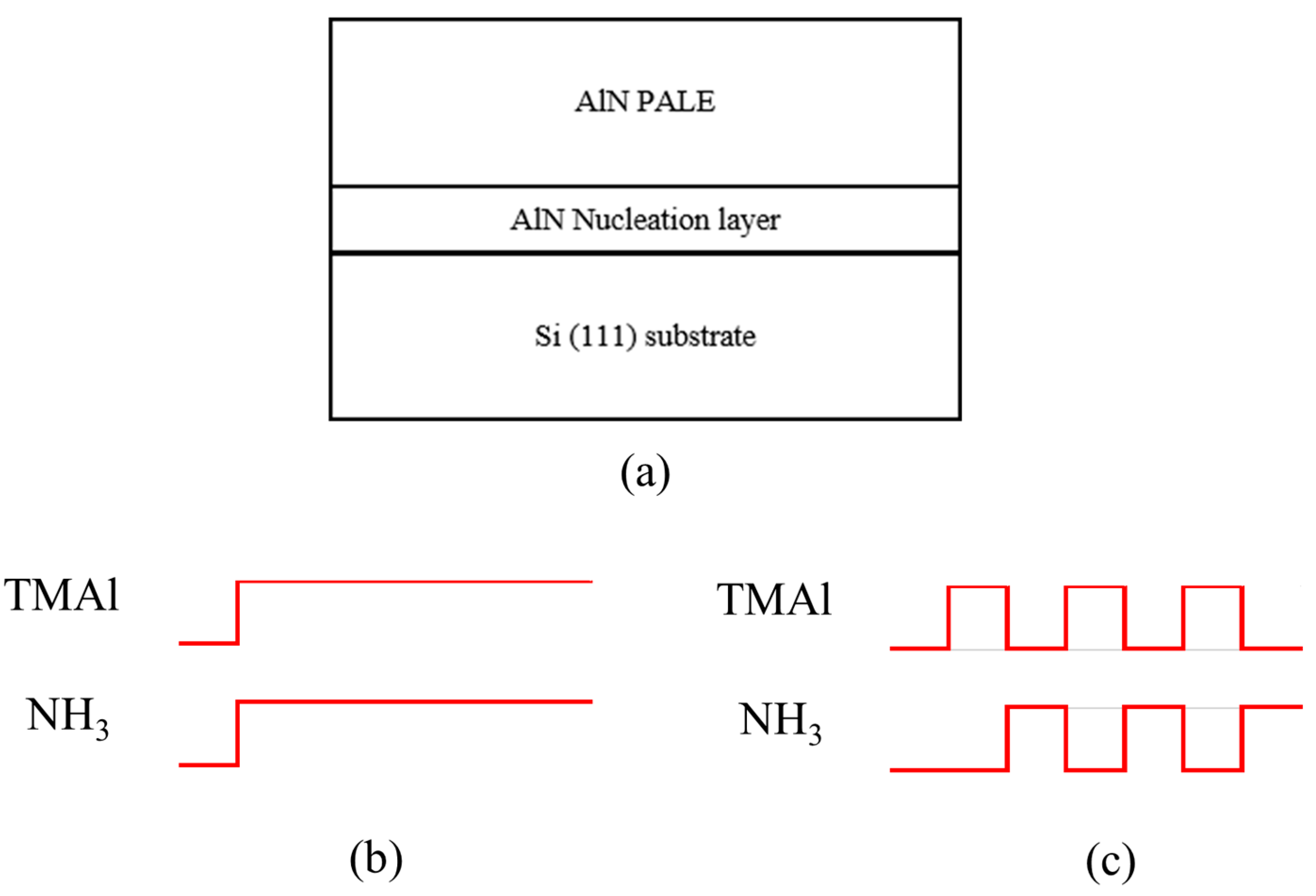
2. Experimental Procedures

In this study, AlN epitaxial films were grown on 2-inch Si (111) substrates. A horizontal flow SR-2000 Taiyo Nippon Sanso metal–organic chemical vapour deposition (MOCVD) system was employed to facilitate the epitaxy process. The schematic growth structure is presented in Figure 1a. Trimethylaluminium (TMAl) and ammonia (NH3) were used as a precursor for Al and N, respectively, while hydrogen (H2) acted as a carrier gas. The substrate initially underwent the Radio Corporation of America (RCA) cleaning procedure, followed by a 2 min etch in buffered hydrofluoric acid (HF) to remove the native oxide from the substrate surface [26]. Prior to the growth, the substrate was subjected to H2 cleaning with a flow rate of 9.5 SLM at 1125 °C for 10 min. Throughout the growth process, the reactor pressure was maintained at 100 Torr. The growth on Si (111) began with 100 nm of AlN nucleation layer at 1000 °C, by simultaneously feeding the Al and N precursor into the reactor, with gas flow rate of 40.63 µmol/min and 5 SLM, respectively. Subsequently, the AlN films were grown at 1180 °C, employing the PMOCVD technique. Growth was achieved by alternately feeding the TMAl and NH3 for 4s and 2s, respectively. The fluxes of the TMAl and NH3 were set as 12.19 µmol/min and 1.8 SLM, respectively. A graphical sequence of the precursor feeding for the nominal and PMOCVD techniques are illustrated in Figure 1b,c, respectively. To investigate the influence of pulsed cycle numbers towards the properties of as-grown AlN epilayers, 0, 35, 70 and 140 cycle numbers were used.
Field emission scanning electron microscopy (FESEM—Hitachi Su8220) (Tokyo, Japan) and atomic force microscopy (AFM—Park System NX-10) (Suwon, Republic of Korea) were utilised to examine the surface morphological properties of the as-grown AlN epilayers. The polarity of the PMOCVD-grown AlN was examined by potassium hydroxide (KOH) wet etching with 0.18 mol/L KOH at 55 °C for 5 min. FESEM cross-sectional analysis and X-ray reflectivity (XRR) measurement were utilised to observe the thickness of the AlN. Then, the samples were subjected to rocking curve measurements using high-resolution X-ray diffraction (HR-XRD—Rigaku Smartlab) (Tokyo, Japan) to analyse the crystalline quality of the samples. HR-XRD was then utilised to study the strain relaxation of the samples by examining the reciprocal space mapping (RSM) of AlN epilayers.

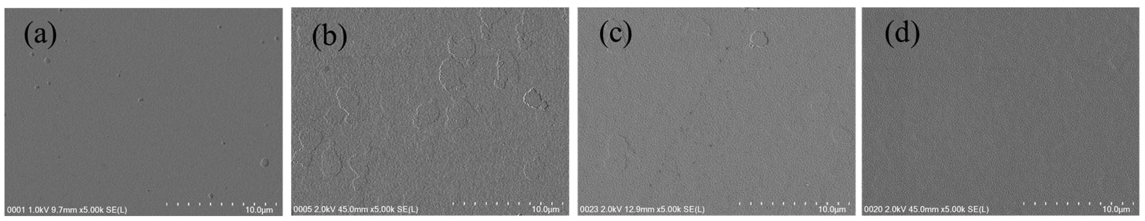
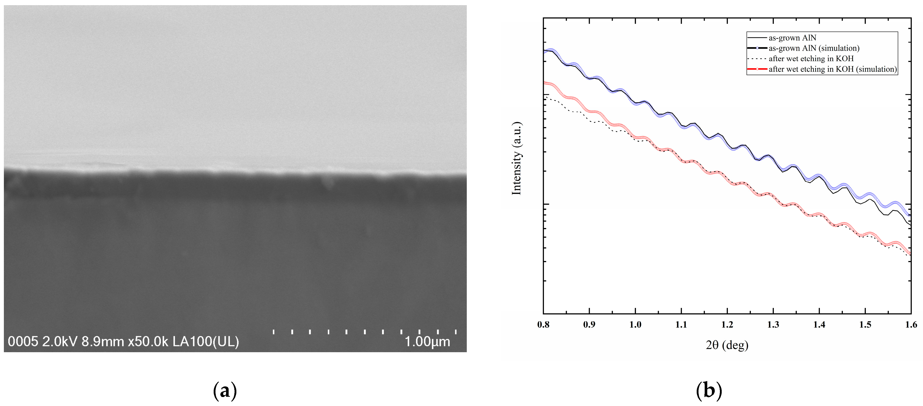
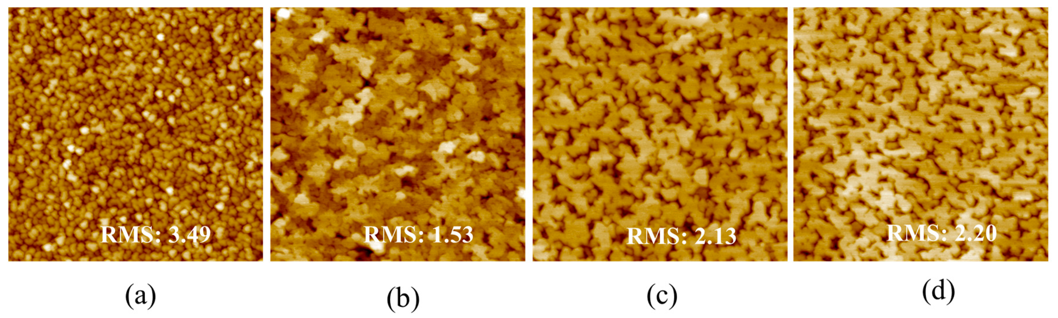
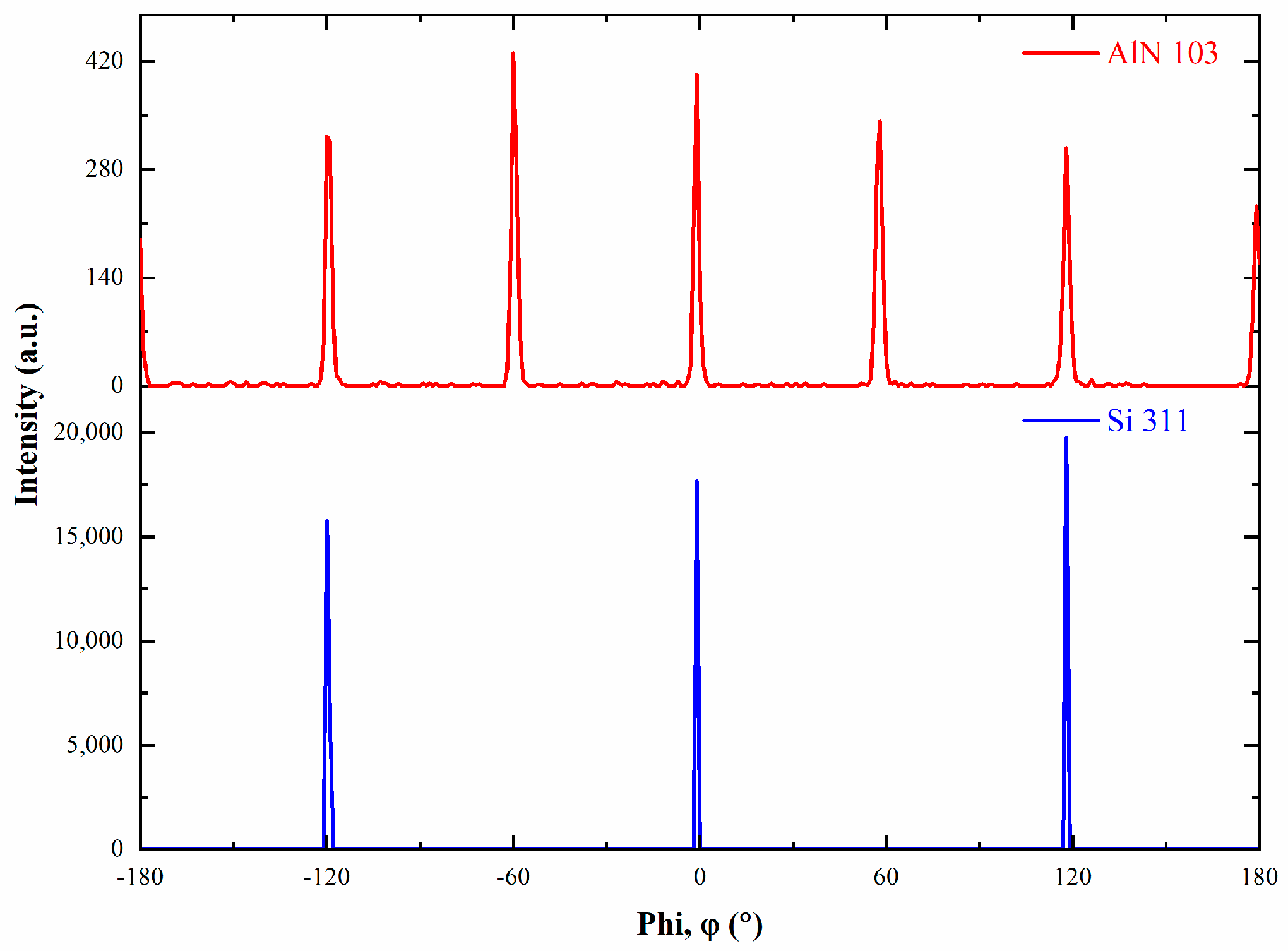
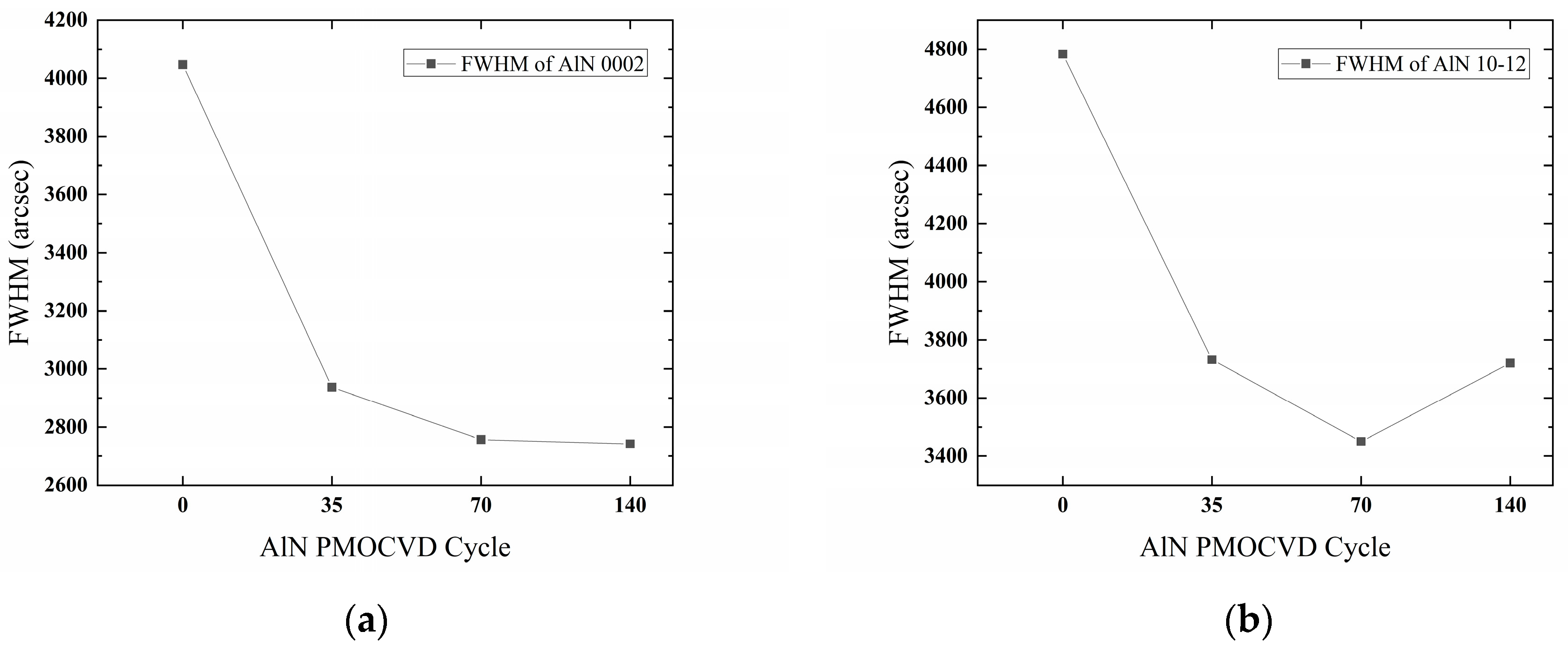
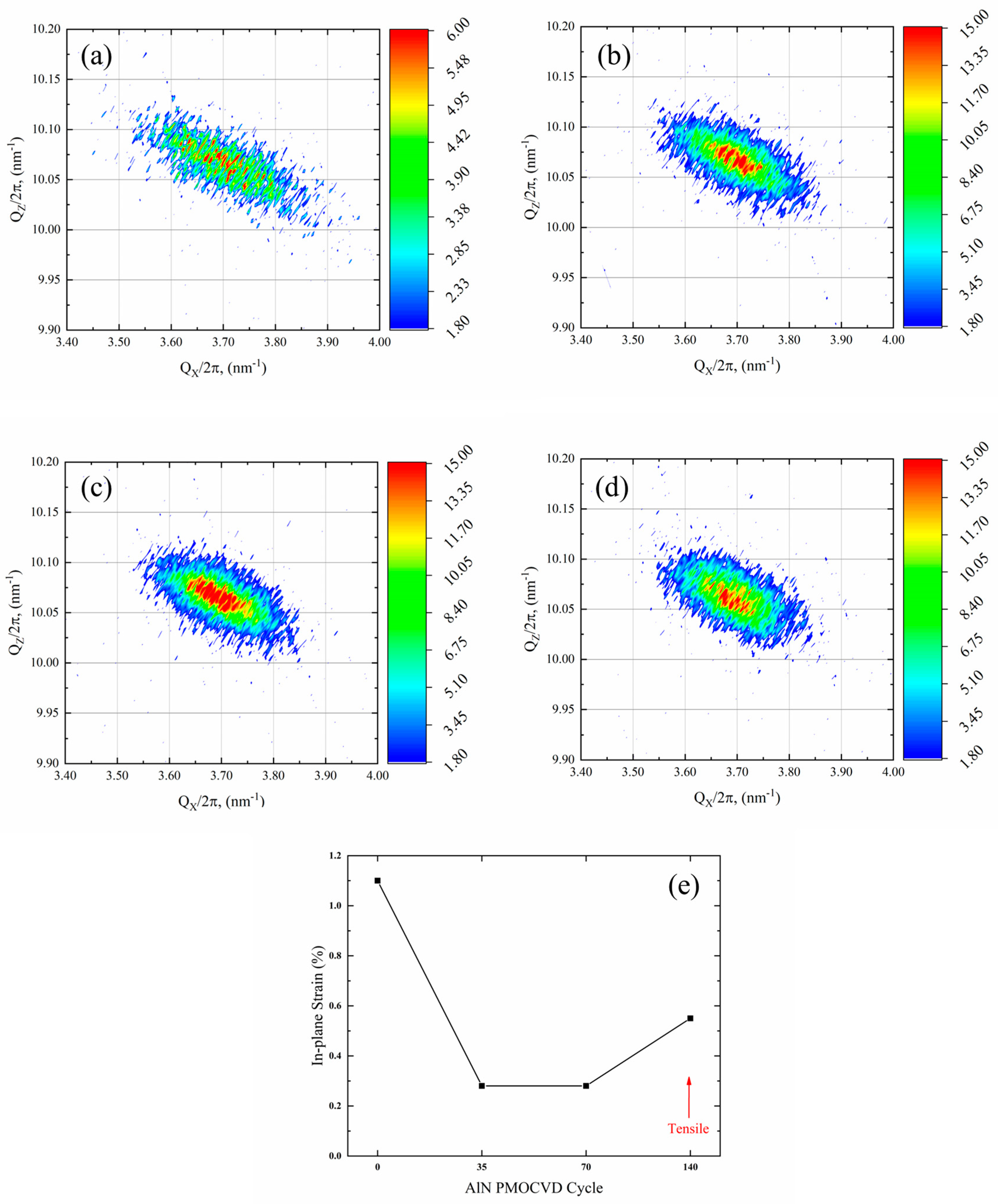
3. Results and Discussions

To analyse the surface properties of the as-grown AlN films, the samples were subjected to the FESEM characterisation. Figure 2 shows the FESEM surface images of the AlN films with different PMOCVD cycle numbers under 5000 times magnification. The evolution in morphology can be clearly seen from the images, where the occasional void area is observed on samples with a low PMOCVD cycle number. At 0 cycle number, small voids were observed, which were non-uniformly distributed on the surface of the epilayers. The low mobility of the Al adatoms in the nominally-grown AlN layer may have contributed to the void observed on the surface of the AlN at 0 PMOCVD cycle number. As the PMOCVD cycle number increases to 35 and 70, the surfaces grow denser as the void becomes bigger and reduces in density. Finally, a dense and flat surface covering the entire samples is seen at 140 cycle number. It is noteworthy that the enhanced augmentation of Al adatoms using the PMOCVD approach promoted quicker grain coalescence in the early phases of the deposition, resulting in extremely uniform and dense surfaces of AlN epilayers [23].
To further analyse the surface properties of the as-grown AlN epilayers, the AFM images with a scan area of 2 µm × 2 µm for the AlN films grown with different PMOCVD cycle numbers are presented in Figure 3. High density and fine grain islands were observed at 0 AlN PMOCVD cycle, which suggests that the growth is under three-dimensional growth mode. As the cycle number increased, it became apparent that the grain island was enlarged and becoming less dense. A 4s interruption of the NH3 supply encouraged the accumulation of Al adatoms on the surface, resulting in larger grains and lower island density [27]. Owing to the gradual increase in the island’s grain size, the grain boundaries of the AlN epilayers grew obscure, forming an atomically flat surface. As a result, the corresponding RMS roughness of the AlN films from 0 to 35 PMOCVD cycle number decreased significantly from 3.49 to 1.53 nm, suggesting that the quasi-two-dimensional growth mode was achieved. This demonstrates that the PMOCVD growth technique enhances the augmentation of Al adatoms and promotes the coalescence surface ratio of the AlN films. However, RMS roughness was observed to increase slightly for 70 and 140 cycle numbers, with corresponding values of 2.13 and 2.20 nm, respectively. During the early coalescence of the AlN islands, the Al adatoms had sufficient mobility to relocate to energetically favourable sites, resulting in randomly sized AlN islands. As the PMOCVD cycle number increased, this caused the growth of some larger grain islands to suppress the smaller ones, mildly increasing the RMS value of the AlN films [14,23].
Figure 4a shows the cross-sectional FESEM of AlN with 70 cycle numbers. The AlN films cover the substrate surfaces and show an abrupt interface between the substrate and the epitaxial layer. The mean measured thickness is 154 nm with an estimated growth rate of 0.5 µm/h. Wet etching by KOH is commonly employed to determine the polarity of AlN. The etch rates can determine the polarity of AlN, with the N-polar typically having a higher etch rate, while in the Al-polar, the etch speed is negligible [28]. In this work, a sample with 70 cycle numbers was exclusively used to determine the polarity of the AlN grown by PMOCVD. Figure 4b shows the XRR measurement along with simulated curves for the AlN with 70 cycle numbers before and after KOH wet etching. The curves are fitted using Rigaku Smartlab Studio II (ver.4.3.200.0). In the simulation, two layers were assumed including the Si (111) substrate and 154 nm AlN. The fitting curves reveal that the thickness of the AlN before and after KOH wet etching are 150.0 and 149.8, respectively, close to the thickness observed in the FESEM cross-sectional analysis. The thickness of the AlN shows no significant reduction after the KOH wet etching process, indicating that the AlN is in the Al-polar.
Thereafter, the crystalline properties of the as-grown AlN epilayers were analysed by HR-XRD using a Cu Kα1 X-ray source with wavelength, λ, of 1.5406 Å. The sample with 70 PMOCVD cycle number 70 was exclusively subjected to a phi, φ scan. Figure 5 shows the φ scan of the AlN 10–13, which reveals the sixfold rotational symmetry separated by 60°, indicating that the film is a single crystalline hexagonal AlN [29]. For Si 311, the φ scan shows the three-fold rotational diffraction peaks with intervals of 120°. This observation confirms the in-plane relationship of the epitaxial growth between AlN [1100] and Si [112] [30,31]. In addition, researchers commonly employed a ω-scan, also known as X-ray rocking curve (XRC) measurement, to investigate the crystalline quality of epitaxial films. The full width at half maximum (FWHM) of the XRC measurements are often used to characterize the structural perfection and degree of crystallinity. At higher degrees of crystalline perfection, a perfectly aligned lattice structure will result in more coherent diffracted X-ray from the crystalline lattice structure, which concurrently reduces the FWHM width [32]. Conversely, wider FWHM suggests a greater degree of imperfection. The imperfection in crystal structure may have originated from lattice defects, threading dislocations, and grain boundaries. These imperfections disrupt the regular arrangement of the lattice structure, leading to the scattering of diffracted X-ray over an angle.
Figure 6a shows the FWHM of AlN 0002, a remarkable decrease in FWHM value is observed as the cycle number increases from 0 to 70 cycles, from 4046 arcsec to 2756 arcsec. Nevertheless, when the cycle number increases to 140, the decreasing trend becomes almost saturated. A similar trend is observed for AlN 10–12 for the cycle numbers from 0 to 70 as the FWHM value dramatically reduces from 4783 arcsec to 3450 arcsec. However, a further increase to 140 cycle number monotonous increase to 3720 arcsec (see Figure 6b). These observations suggest that the AlN epilayers’ crystalline quality are significantly improved due to the introduction of the PMOCVD technique in the epitaxial structure. The FWHM results of AlN 0002 are comparable with the other AlN growth reports using various techniques as listed in Table 1 [15,25]. The narrowest FWHM observed at 70 cycle indicates that the crystalline quality of the as-grown AlN epilayer have a higher degree of crystalline imperfection with a well-defined lattice structure. The broadening of FWHM with a prolonged PMOCVD cycle from 70 to 140 may have resulted from the increase in the surface roughness as observed in the AFM measurement. During the coalescence of the AlN grain island, the growth of the larger grain island may surpass the smaller one and will induce threading dislocations in the epitaxial layer [33]. The Al–N bond in the c-direction of the hexagonal AlN crystal structure is stronger than the three in-plane bonds, increasing the likelihood of rotation in the mosaic structure and ultimately, increasing the diffracted X-ray scattering and XRC peak widening.
Furthermore, reciprocal space mapping (RSM) measurements of AlN 10–15 were performed to further understand the crystallography properties of the AlN epilayers deposited at different PMOCVD cycle numbers, as presented in Figure 7a–d. From the RSM measurements, the information on the lattice constants a and c of the AlN epilayers can be calculated via [34,35]:
a = 2 π Q x 4 ( h 2 + h k + k 2 ) 3
c = 2 π l Q z
where hkl are the Miller indices of AlN 10–15 reflection (in this case, h = 1, k = 0, l = 5). Using the calculated lattice constant for a and c for the AlN epilayers, the in-plane (εxx) and out-of-plane (εzz) strain of the layers can be calculated using:
ε x x = a a 0 a 0
ε z z = c c 0 c 0
where a and c were the measured lattice constants, while a 0 = 3.112 Å and c 0 = 4.982 Å, represent the free-standing lattice constant of AlN. The calculated value from the RSM measurement of AlN 10–15 measurements were tabulated in Table 2.
Figure 7e shows the in-plane strain of the AlN epilayers as a function of the PMOCVD cycle number. It can be observed that all the samples were in tensile strain. As the PMOCVD cycle number increased from 0 to 35 and 70, the in-plane strain value decreased from 1.10%, 0.28%, and 0.28%, respectively. Nevertheless, a marginal increase to 0.55% was observed at 140 PMOCVD cycle. The difference in thermal expansion coefficient between the AlN and Si (111) substrate during the cooling phase from growth to room temperature was the primary cause of tensile strain [36]. In addition, tensile stress was also built up during the growth process due to the lattice mismatch, which promoted the propagation of threading dislocations [37]. Eventually, the reduction in the FWHM width observed in the XRC measurement followed the same pattern as the decrease in the in-plane tensile strain observed in the RSM measurement. At 140 cycle number, the presence of strain may cause the broadening of the FWHM of the XRC, due to the variation in lattice constant caused by the lattice strain-induced distortion. Thus, this finding indicates that the PMOCVD cycle number has a major influence on the stress modulation during the growth and cooling processes of the AlN epilayers.

4. Conclusions

This study discussed the relationship between the AlN PMOCVD cycle number and the morphological and structural properties of AlN-on-Si (111) substrate via MOCVD. The study revealed that the morphological and structural properties critically depended on the AlN PMOCVD cycle number. Field emission scanning electron microscopy revealed void-less and dense surfaces of AlN epilayers at the highest PMOCVD cycle number. Additionally, according to atomic force microscopy, the AlN grain islands enlarged and showed a quasi-two-dimensional growth mode with the incorporation of PMOCVD method. The Al-polar of the AlN epitaxial layer is confirmed by the KOH wet etching procedure. Furthermore, the width of FWHM for AlN 0002 and 10–12 decreased concurrently with the increased PMOCVD cycle number, indicating an improvement in crystalline quality. In addition, reciprocal space mapping of AlN 10–15 showed that the in-plane tensile strain in the AlN epilayers was inversely proportional to the PMOCVD cycle number. The optimised AlN epilayers were observed at 70 cycle number with the narrowest FWHM of AlN 0002, 10–12, and in-plane tensile strain of 2756 arcsec, 3450 arcsec, and 0.28%, respectively. Hence, the PMOCVD growth methodology is advantageous and may be used as an alternate method for the growth of high-quality AlN-on-Si (111) epitaxy.

Author Contributions

Conceptualization, M.I.H.; Methodology, M.I.H.; Investigation, M.I.H.; Writing—Original Draft, M.I.H.; Writing—Review and Editing, R.N.; Supervision, A.S.; Funding acquisition, A.S.; Visualization, M.M.; Validations, A.W.; Formal Analysis, M.R.M.H. All authors have read and agreed to the published version of the manuscript.

Funding

This work was funded by the High Efficiency High Electron Mobility Transistor (HEMT) for Power Electronics Modules (MOSTI005-2021SRF/SRF-APP PG1-P3) granted by the Malaysia Ministry of Science, Technology and Innovation (MOSTI); Gallium Nitride Vertical Power Metal-Insulator-Semiconductor Field Effect Transistor (CREST/R&D/T(G-E)03-22/003) and Vapour Phase Epitaxy (VPE) Technology Research for GaN-on-Si High Electron Mobility Transistor (PV007-2019/T13C2-17) granted by Collaborative Research in Engineering, Science and Technology Center (CREST); Low Temperature Flow Modulation Epitaxy for AlInGaN Growth, Packaging and Deployment of DUV LEDs (PV058-2023) granted by Universiti Malaya(UM)-CREST matching grant.

Data Availability Statement

The original contributions presented in the study are included in the article, further inquiries can be directed to the corresponding author.

Acknowledgments

The authors would like to thank the members of the Nitride Epitaxy and Nanofabrication (Universiti Malaya) for their support throughout the experiment.

Conflicts of Interest

Adam Williams is employed by the company Silterra Malaysia Sdn. Bhd., Lot 8, Phase II Kulim Hi-Tech Park, and Mohd Rofei Mat Hussin is employed by the company MIMOS Berhad, Technology Park Malaysia. The remaining authors declare that the research was conducted in the absence of any commercial or financial relationships that could be construed as a potential conflict of interest.

References

  1. Pengelly, R.S.; Wood, S.M.; Milligan, J.W.; Sheppard, S.T.; Pribble, W.L. A Review of GaN on SiC High Electron-Mobility Power Transistors and MMICs. IEEE Trans. Microw. Theory Tech. 2012, 60, 1764–1783. [Google Scholar] [CrossRef]
  2. Fletcher, A.S.A.; Nirmal, D. A Survey of Gallium Nitride HEMT for RF and High-Power Applications. Superlattices Microstruct. 2017, 109, 519–537. [Google Scholar] [CrossRef]
  3. Zhu, D.; Wallis, D.J.; Humphreys, C.J. Prospects of III-Nitride Optoelectronics Grown on Si. Rep. Prog. Phys. 2013, 76, 106501. [Google Scholar] [CrossRef] [PubMed]
  4. Nagamatsu, K.; Okada, N.; Sugimura, H.; Tsuzuki, H.; Mori, F.; Iida, K.; Bando, A.; Iwaya, M.; Kamiyama, S.; Amano, H.; et al. High-Efficiency AlGaN-Based UV Light-Emitting Diode on Laterally Overgrown AlN. J. Cryst. Growth 2008, 310, 2326–2329. [Google Scholar] [CrossRef]
  5. Inoue, Y.; Nagasawa, H.; Sone, N.; Ishino, K.; Ishida, A.; Fujiyasu, H.; Kim, J.J.; Makino, H.; Yao, T.; Sakakibara, S.; et al. Fabrication and Characterization of Short Period AlN/GaN Quantum Cascade Laser Structures. J. Cryst. Growth 2004, 265, 65–70. [Google Scholar] [CrossRef]
  6. Dadgar, A.; Poschenrieder, M.; Asing, J.B.; Contreras, O.; Bertram, F.; Riemann, T.; Reiher, A.; Kunze, M.; Daumiller, I.; Krtschil, A.; et al. MOVPE Growth of GaN on Si (111) Substrates. J. Cryst. Growth 2003, 248, 556–562. [Google Scholar] [CrossRef]
  7. Freedsman, J.J.; Watanabe, A.; Yamaoka, Y.; Kubo, T.; Egawa, T. Influence of AlN Nucleation Layer on Vertical Breakdown Characteristics for GaN-on-Si. Phys. Status Solidi A 2016, 213, 424–428. [Google Scholar] [CrossRef]
  8. Zhang, B.S.; Wu, M.; Shen, X.M.; Chen, J.; Zhu, J.J.; Liu, J.P.; Feng, G.; Zhao, D.G.; Wang, Y.T.; Yang, H. Influence of High-Temperature AIN Buffer Thickness on the Properties of GaN Grown on Si (111). J. Cryst. Growth 2003, 258, 34–40. [Google Scholar] [CrossRef]
  9. Kim, J.O.; Hong, S.K.; Lim, K.Y. Crack Formation in GaN on Si (111) Substrates Grown by MOCVD Using HT Al-preseeding and HT AlN Buffer Layers. Phys. Status Solidi C 2010, 7, 2052–2055. [Google Scholar] [CrossRef]
  10. Li, F.; Wang, L.; Yao, W.; Meng, Y.; Yang, S.; Wang, Z. Analysis of Growth Rate and Crystal Quality of AlN Epilayers by Flow-Modulated Metal Organic Chemical Vapor Deposition. Superlattices Microstruct. 2020, 137, 106336. [Google Scholar] [CrossRef]
  11. Huang, L.; Li, Y.; Wang, W.; Li, X.; Zheng, Y.; Wang, H.; Zhang, Z.; Li, G. Growth of High-Quality AlN Epitaxial Film by Optimizing the Si Substrate Surface. Appl. Surf. Sci. 2018, 435, 163–169. [Google Scholar] [CrossRef]
  12. Wang, D.; Uesugi, K.; Xiao, S.; Norimatsu, K.; Miyake, H. High-Quality AlN/Sapphire Templates Prepared by Thermal Cycle Annealing for High-Performance Ultraviolet Light-Emitting Diodes. Appl. Phys. Express 2021, 14, 035505. [Google Scholar] [CrossRef]
  13. Arulkumaran, S.; Egawa, T.; Matsui, S.; Ishikawa, H. Enhancement of Breakdown Voltage by AlN Buffer Layer Thickness in AlGaNGaN High-Electron-Mobility Transistors on 4 in. Diameter Silicon. Appl. Phys. Lett. 2005, 86, 123503. [Google Scholar] [CrossRef]
  14. Wang, H.; Li, S.L.; Xiong, H.; Wu, Z.H.; Dai, J.N.; Tian, Y.; Fang, Y.Y.; Chen, C.Q. The Effect of AlN Nucleation Temperature on the Growth of AlN Films via Metalorganic Chemical Vapor Deposition. J. Electron. Mater. 2012, 41, 466–470. [Google Scholar] [CrossRef]
  15. Feng, Y.; Wei, H.; Yang, S.; Chen, Z.; Wang, L.; Kong, S.; Zhao, G.; Liu, X. Competitive Growth Mechanisms of AlN on Si (111) by MOVPE. Sci. Rep. 2014, 4, 6416. [Google Scholar] [CrossRef] [PubMed]
  16. Hirayama, H.; Maeda, N.; Fujikawa, S.; Toyoda, S.; Kamata, N. Recent progress and future prospects of AlGaN-based high-efficiency deep-ultraviolet light-emitting diodes. Jpn. J. Appl. Phys. 2014, 53, 100209. [Google Scholar] [CrossRef]
  17. Zhang, J.P.; Asif Khan, M.; Sun, W.H.; Wang, H.M.; Chen, C.Q.; Fareed, Q.; Kuokstis, E.; Yang, J.W. Pulsed atomic layer epitaxy of ultrahigh-quality AlxGa1-xN structures for deep ultraviolet emissions below 230 nm. Appl. Phys. Lett. 2002, 81, 4392–4394. [Google Scholar] [CrossRef]
  18. Xue, J.; Zhang, J.; Hao, Y. Ultrathin barrier AlN/GaN high electron mobility transistors grown at a dramatically reduced growth temperature by pulsed metal organic chemical vapor deposition. Appl. Phys. Lett. 2015, 107, 043503. [Google Scholar] [CrossRef]
  19. Hirayama, H.; Yatabe, T.; Noguchi, N.; Ohashi, T.; Kamata, N. 231–261 nm AlGaN deep-ultraviolet light-emitting diodes fabricated on AlN multilayer buffers grown by ammonia pulsed-flow method on sapphire. Appl. Phys. Lett. 2007, 91, 071901. [Google Scholar] [CrossRef]
  20. Hirayama, H.; Fujikawa, S.; Noguchi, N.; Norimatsu, J.; Takano, T.; Tsubaki, K.; Kamata, N. 222–282 nm AlGaN and InAlGaN-based deep-UV LEDs fabricated on high quality AlN on sapphire. Phys. Status Solidi A 2009, 206, 1176–1182. [Google Scholar] [CrossRef]
  21. Abd Rahman, M.N.; Shuhaimi, A.; Abdul Khudus, M.I.M.; Anuar, A.; Zainorin, M.Z.; Talik, N.A.; Chanlek, N.; Abd Majid, W.H. Diminishing the Induced Strain and Oxygen Incorporation on Aluminium Nitride Films Deposited Using Pulsed Atomic-Layer Epitaxy Techniques at Standard Pressure MOCVD. J. Electron. Mater. 2021, 50, 2313–2322. [Google Scholar] [CrossRef]
  22. Abd Rahman, M.N.; Talik, N.A.; Abdul Khudus, M.I.M.; Sulaiman, A.F.; Allif, K.; Zahir, N.M.; Shuhaimi, A. Ammonia Flux Tailoring on the Quality of AlN Epilayers Grown by Pulsed Atomic-Layer Epitaxy Techniques on (0001)-Oriented Sapphire Substrates via MOCVD. CrystEngComm 2019, 21, 2009–2017. [Google Scholar] [CrossRef]
  23. Abd Rahman, M.N.; Yusuf, Y.; Anuar, A.; Mahat, M.R.; Chanlek, N.; Talik, N.A.; Abdul Khudus, M.I.M.; Zainal, N.; Abd Majid, W.H.; Shuhaimi, A. Agglomeration Enhancement of AlN Surface Diffusion Fluxes on a (0001)-Sapphire Substrate Grown by Pulsed Atomic-Layer Epitaxy Techniques: Via MOCVD. CrystEngComm 2020, 22, 3309–3321. [Google Scholar] [CrossRef]
  24. Rahman, M.N.A.; Sulaiman, A.F.; Khudus, M.I.M.A.; Allif, K.; Talik, N.A.; Basri, S.H.; Shuhaimi, A. Effects of Pulsed Cycle Number on the Quality of Pulsed Atomic-Layer Epitaxy AlN Films Grown via Metal Organic Chemical Vapor Deposition. Jpn. J. Appl. Phys. 2019, 58, SC1037. [Google Scholar] [CrossRef]
  25. Altuntas, I.; Kocak, M.N.; Yolcu, G.; Budak, H.F.; Kasapoğlu, A.E.; Horoz, S.; Gür, E.; Demir, I. Influence of the PALE Growth Temperature on Quality of MOVPE Grown AlN/Si (111). Mater. Sci Semicond. Process. 2021, 127, 105733. [Google Scholar] [CrossRef]
  26. Simsek, I.; Yolcu, G.; Koçak, M.N.; Pürlü, K.; Altuntas, I.; Demir, I. Nucleation Layer Temperature Effect on AlN Epitaxial Layers Grown by Metalorganic Vapour Phase Epitaxy. J. Electron. Mater. 2021, 32, 25507–25515. [Google Scholar] [CrossRef]
  27. Abd Rahman, M.N.; Shuhaimi, A.; Yusuf, Y.; Li, H.; Sulaiman, A.F.; Alif Samsudin, M.E.; Zainal, N.; Abdul Khudus, M.I.M. Standard Pressure Deposition of Crack-Free AlN Buffer Layer Grown on c-Plane Sapphire by PALE Technique via MOCVD. Superlattices Microstruct. 2018, 120, 319–326. [Google Scholar] [CrossRef]
  28. Zhang, H.; Persson, I.; Papamichail, A.; Chen Jr., T.; Persson, P.O.A.; Paskov, P.P.; Darakcieva, V. On the polarity determination and polarity inversion in nitrogen-polar group III-nitride layers grown on SiC. J. Appl. Phys. 2022, 131, 055701. [Google Scholar] [CrossRef]
  29. Arslan, E.; Ozturk, M.K.; Duygulu, Ö.; Kaya, A.A.; Ozcelik, S.; Ozbay, E. The influence of nitridation time on the structural properties of GaN grown on Si (111) substrate. Appl. Phys. A 2009, 94, 73–82. [Google Scholar] [CrossRef]
  30. Wang, W.; Yang, W.; Liu, Z.; Wang, H.; Wen, L.; Li, G. Interfacial Reaction Control and Its Mechanism of AlN Epitaxial Films Grown on Si (111) Substrates by Pulsed Laser Deposition. Sci. Rep. 2015, 5, 11480. [Google Scholar] [CrossRef]
  31. Li, Y.; Wang, W.; Li, X.; Huang, L.; Zheng, Y.; Chen, X.; Li, G. Nucleation Layer Design for Growth of a High-Quality AlN Epitaxial Film on a Si (111) Substrate. CrystEngComm 2018, 20, 1483–1490. [Google Scholar] [CrossRef]
  32. Masiello, F.; Cembali, G.; Chumakov, A.I.; Connel, S.H.; Ferrero, C.; Hartwig, J.; Sergeev, I.; Vaerenbergh, P.V. Rocking curve measurement revisited. J. Appl. Cryst. 2014, 47, 1304–1314. [Google Scholar] [CrossRef]
  33. Fan, R.; Zhi-Bao, H.; Jian-Nan, H.; Chen, Z.; Yi, L. Effects of AlN nucleation layer thickness on crystal quality of AlN grown by plasma-assisted molecular beam epitaxy. Chin. Phys. B 2010, 19, 116801. [Google Scholar]
  34. Lee, H.P.; Perozek, J.; Rosario, L.D.; Bayram, C. Investigation of AlGaN/GaN High Electron Mobility Transistor Structures on 200-Mm Silicon (111) Substrates Employing Different Buffer Layer Configurations. Sci. Rep. 2016, 6, 37588. [Google Scholar] [CrossRef] [PubMed]
  35. Feng, Y.; Saravade, V.; Chung, T.F.; Dong, Y.; Zhou, H.; Kucukgok, B.; Ferguson, I.T.; Lu, N. Strain-Stress Study of AlxGa1−xN/AlN Heterostructures on c-Plane Sapphire and Related Optical Properties. Sci. Rep. 2019, 9, 10172. [Google Scholar] [CrossRef] [PubMed]
  36. Wang, K.; Li, M.; Yang, Z.; Wu, J.; Yu, T. Stress Control and Dislocation Reduction in the Initial Growth of GaN on Si (111) Substrates by Using a Thin GaN Transition Layer. CrystEngComm 2019, 21, 4792–4797. [Google Scholar] [CrossRef]
  37. Pan, L.; Dong, X.; Li, Z.; Luo, W.; Ni, J. Influence of the AlN Nucleation Layer on the Properties of AlGaN/GaN Heterostructure on Si (1 1 1) Substrates. Appl. Surf. Sci. 2018, 447, 512–517. [Google Scholar] [CrossRef]
Figure 1. (a) The schematic cross-sectional view of AlN-on-Si (111) substrate. The gas flow used for TMAl and NH3 using the (b) nominal and (c) PMOCVD growth technique.
Crystals 14 00371 g001
Figure 2. FESEM surface image with different PMOCVD cycle numbers (a) 0, (b) 35, (c) 70, and (d) 140.
Crystals 14 00371 g002
Figure 3. 2 µm × 2 µm AFM images of AlN epilayers with different PMOCVD cycle number (a) 0, (b) 35, (c) 70, and (d) 140.
Crystals 14 00371 g003
Figure 4. (a) FESEM cross-sectional images of AlN with 70 cycle numbers, (b) XRR and its simulated curves for 70 cycle PMOCVD AlN before and after KOH wet etching.
Crystals 14 00371 g004
Figure 5. HR-XRD phi, φ scan for AlN 10−13 and Si 311 of the sample with 70 PMOCVD cycles.
Crystals 14 00371 g005
Figure 6. The dependence of PMOCVD cycle number towards the FWHM of (a) AlN 0002 and (b) AlN 10–12.
Crystals 14 00371 g006
Figure 7. XRD reciprocal space mapping (RSM) of AlN 10–15 for the AlN epilayers grown on the Si (111) substrate with (a) 0, (b) 35, (c) 70, and (d) 140 PMOCVD cycle number. (e) The in-plane strain of the AlN epilayers as a function of PMOCVD cycle number.
Crystals 14 00371 g007
Table 1. List of reported FWHM of AlN 0002 using various growth techniques.
No.TitleGrowth TechniqueFWHM of AlN 0002References
1.This workPMOCVD0.76°
2.Influence of PALE growth temperature on quality of MOVPE grown AlN/Si (111)PALE1.53°[25]
3.Competitive growth mechanisms of AlN on Si (111) by MOVPEMass transport mechanism0.68°[15]
Table 2. The summary of XRD reciprocal space mapping (RSM) of AlN 10–15 calculation.
PMOCVD Cycle NumberIn-Plane Lattice ParameterOut-of-Plane Lattice Parameter
Qx/2π (nm−1)a (Å)Strain (%)Qz/2π (nm−1)c (Å)Strain (%)
03.673.151.1010.084.96−0.44
353.703.120.2810.074.97−0.34
703.703.120.2810.074.97−0.34
1403.693.130.5510.064.97−0.24
Disclaimer/Publisher’s Note: The statements, opinions and data contained in all publications are solely those of the individual author(s) and contributor(s) and not of MDPI and/or the editor(s). MDPI and/or the editor(s) disclaim responsibility for any injury to people or property resulting from any ideas, methods, instructions or products referred to in the content.

