Article

High-Efficiency Vertical-Chip Micro-Light-Emitting Diodes via p-GaN Optimization and Surface Passivation

by
Yizhou Qian
1,
En-Lin Hsiang
1,
Yu-Hsin Huang
2,
Kuan-Heng Lin
2 and
Shin-Tson Wu
1,*
1
College of Optics and Photonics, University of Central Florida, Orlando, FL 32816, USA
2
AUO Corporation, Hsinchu Science Park, Hsinchu 300, Taiwan
*
Author to whom correspondence should be addressed.
Crystals 2024, 14(6), 503; https://doi.org/10.3390/cryst14060503
Submission received: 25 April 2024 / Revised: 21 May 2024 / Accepted: 23 May 2024 / Published: 25 May 2024
(This article belongs to the Section Organic Crystalline Materials)

Abstract

:
Micro-LEDs have found widespread applications in modular large-screen TVs, automotive displays, and high-resolution-density augmented reality glasses. However, these micron-sized LEDs experience a significant efficiency reduction due to the defects originating from the dry etching process. By controlling the current distribution via engineering the electrode size, electrons will be less concentrated in the defect region. In this work, we propose a blue InGaN/GaN compound parabolic concentrator micro-LED with a metallic sidewall to boost efficiency by combining both an optical dipole cloud model and electrical TCAD (Technology Computer-Aided Design) model. By merely modifying the p-GaN contact size, the external quantum efficiency (EQE) can be improved by 15.6%. By further optimizing the passivation layer thickness, the EQE can be boosted by 52.1%, which helps enhance the display brightness or lower power consumption.

1. Introduction

Lately, micro-LEDs (light-emitting diodes) have found widespread applications in modular large-screen TVs [1], automotive displays [2], and augmented reality (AR) glasses [3] due to their small mesa size, ultra-high brightness, excellent thermal stability, perfect dark state, and long lifetime [4,5,6,7,8]. Still, the requirement to produce full-color ultra-small μLED chips with high efficiency is demanding [9,10]. For transparent head-up displays in vehicles, μLEDs with a mesa size smaller than 20 μm and luminance over 3000 nits are required to maintain a high ambient contrast ratio under direct sunlight [11]. For lightweight AR glasses, the μLED light engine is usually imbedded in the temple. Therefore, the pixel size should be smaller than 5 μm in order to achieve high resolution density in a tiny (<0.2”) microdisplay panel [12]. In addition, to deliver recognizable images to the user under a daylight outdoor environment (e.g., 3000 nits), the digital image brightness of about 10,000 nits is required to offer a minimally acceptable ambient contrast ratio ACR ≥ 3:1. If the losses from the waveguide optical combiner and exit pupil expansion are considered, then the required display luminance would exceed ~1 million nits.
To fabricate such small µLED chips, an accurate dry etching process is often employed when forming the mesas, while the sidewall defects induced by plasma etching will decrease the efficiency significantly [13,14]. Such an efficiency degradation is mainly attributed to the increasing carrier delocalization, which results in a higher surface recombination velocity [15,16]. Several approaches have been developed to circumvent this issue. For example, the wet etching process can remove the damaged material, but the chip size uniformity could be compromised [17]. Surface passivation by the dielectric layer can alleviate the sidewall defects, but this reduces the light-emitting area [18,19]. In 2019, Wong et al. fabricated µLED structures on a patterned sapphire substrate with a varying mesa size from 10 µm × 10 µm to 100 µm × 100 µm. By applying a combination of wet etching and surface passivation, the size effect of µLED is suppressed while keeping a high external quantum efficiency (EQE = 22% to 27%) [20]. Other approaches, such as nanowire µLED chips fabricated by the bottom-up method, can avoid such sidewall damage and achieve an almost size-independent EQE [21,22]. Recent progress shows that red-emitting submicron nanowire InGaN LEDs can achieve an EQE of ~8% at a current density of ~1 A/cm2 [23]. However, the fabrication cost remains to be lowered due to the demanding cleanroom environment.
Except for improving EQE through a fabrication procedure, a controlled current distribution in a µLED can alleviate its size effect. As introduced by Keith et al. [24], modifying the p-GaN contact diameter helps reduce the sidewall recombination and current crowing efficiency losses in a 10 µm diameter µLED. However, optical models should be taken into consideration for calculating the light extraction efficiency (LEE) to provide an accurate geometry-dependent light emission. In 2023, Hsu et al. studied the current confinement effect on a 10 µm × 10 µm µLED array. An optimized EQE of 9.95% is achieved when the electrode contact size is 5 µm × 5 µm. To accurately calculate LEE in a µLED chip, the dipole cloud model considers the active layer in the μLED to be dipole arrays instead of a single dipole in the center [25]. On the other hand, previous works related to the dipole cloud model often neglected the electrical weightage of each dipole, which is far from the realistic case. Therefore, electrical simulations should be performed to provide a more accurate result. As a result, the combination of electrical simulation and the dipole cloud model can provide a more accurate result.
In this paper, we construct a vertical-chip compound parabolic concentrator (CPC) blue InGaN/GaN single-quantum well (SQW) µLED via both optical and electrical simulations. The optical dipole cloud model is built in a commercial wave optics simulation software Finite-Difference Time-Domain (FDTD 2024 R1.3, Ansys Inc., Canonsburg, PA, USA), and electrical simulation is performed in Silvaco technology computer-aided design (TCAD 5.0.10.R, Silvaco Inc., Santa Clara, CA, USA). Then, we investigate the mechanism behind metallic sidewall loss and optimize the reflectance from the metallic sidewall by a dielectric passivation layer to suppress the surface plasmon polariton (SPP) mode. Next, we optimize the CPC µLED with the dipole cloud model to study the position-dependent LEE. To consider the electrical weightage of each dipole, we combine the LEE results with the current distribution based on TCAD. By properly designing the p-GaN contact size, the weightage of the dipoles close to the sidewall can be reduced, which improves the normalized EQE by 15.6%. By further optimizing the dielectric passivation layer’s thickness, SPP loss is suppressed, which in turn dramatically improves the normalized EQE by 52.1%.

2. Simulation Methods

2.1. Optical Model for Blue InGaN/GaN CPC μLED

The vertical-chip cylindrical µLED model with a vertical n-electrode was constructed in 2D-FDTD simulation by employing the CPC structure, which has been widely used to concentrate the light emitted by LEDs [26]. As indicated in Figure 1, the curved CPC shape sidewall is 1-µm Al (n = 0.63 + j5.45 @ λ = 450 nm) coated with a 500-nm SiO2 (n = 1.5) passivation layer. The active region is a layer of 3 nm InGaN SQW, and the electron blocking layer (EBL) is a 50 nm thick AlGaN. The µLED is immersed in polyimide, whose refractive index is 1.5. The p-contact and n-contact are Au and ITO (indium tin oxide), respectively. Although using ITO as an n-contact is not very efficient for electron injection, which in turn increases the driving voltage, its excellent transparency helps to achieve a high LEE. In addition, placing the p-GaN layer under the active layer instead of the thick n-GaN layer is beneficial to optical design freedom. At the top of the structure, the Al sidewall is insulated from the ITO electrode by a 500 nm SiO2 layer to avoid the conduction issue. The dispersion of all the materials and blue light emission spectrum from the QW are all considered [27,28,29]. The boundary condition is a 16-layer steep-angle perfect-matched layer (SA-PML) to absorb all the escaped light. A large 2D emission box monitor is placed around the structure in air to calculate the emission power of the LED. The substrate side of the 2D large box monitor is open to get rid of the substrate loss. Small 2D dipole box monitors are placed surrounding each dipole source to calculate the dipole power. Therefore, the LEE is calculated by the ratio of the emission power to the dipole power. Since the GaN crystal structure is wurtzite, only dipoles oscillating along x- and z-directions are considered, and we denote them as in-plane (I) and out-of-plane (O), respectively.

2.2. LEE Calculation

As reported in [25], in terms of calculating the angular distribution and LEE, the dipole cloud model can provide a more precise result than the traditional center dipole model, although it requires a larger amount of computer memory. In this simulation, the FDTD dipole cloud model is built based on a total of 10 horizontal dipoles simulated in the active region due to circular symmetry. Each dipole is separated by 200 nm along the horizontal axis (x-axis) from the center of the quantum well. The angular distribution of each dipole can be calculated by eliminating the wavelength λ and polarization p (I or O):
A 1 θ , x = p = I , O A θ , x , λ , p , a S ( λ ) d λ 2 S ( λ ) d λ ,
where A is the calculated far-field distribution, θ is the polar angle, S(λ) is the emission spectrum, and x is the distance from the dipole to the center of the quantum well.
For near-eye displays, the accepting cone of the imaging system is typically limited to ±20°. For automotive displays on the driver’s side, such as the head-up display and dashboard panel, the position of the driver’s eyebox is typically fixed, resulting in a preference for quasi-collimated light emission from the display. Therefore, we only consider the effective LEE (LEE20), which is the LEE received within ±20° in the far-field:
η 1 ( x ) = p = I , O k x , λ , p η ( x , λ , p ) S ( λ ) d λ 2 S ( λ ) d λ ,
where λ is the incident wavelength, p is the dipole oscillating direction (I or O), η is the calculated LEE for each dipole, and k is the ±20° spectral coefficient, which can be calculated by integrating the light intensity from the far-field monitor. The total effective LEE of the dipole cloud can be calculated by properly weighting the response from each dipole as follows:
L E E 20 = 0 X η 1 ( θ , φ , x , z ) 2 π x d x π X 2 ,
where X is the radius of the quantum well.

2.3. Electrical Model of CPC μLED

The electrical model is constructed in Silvaco TCAD. Before building the electrical model of our CPC vertical-chip µLED, experimental validation is performed based on the results published by Behrman and Kymissis [24]. Different from our vertical electrode structure, the validating model is a 10 µm SQW InGaN/GaN LED with nGaN contact on the side. As shown in Figure 2, the I–V curve agrees with each other very well when the voltage sweeps from 3.2 V to 4 V.
After the model is validated, we construct our CPC vertical-chip SQW µLED in Silvaco TCAD. Detailed geometry is shown in Figure 1, and doping is listed in Table 1. The thickness of pGaN is optimized by optical simulation, which will be discussed in Section 3.2.

3. Results and Discussion

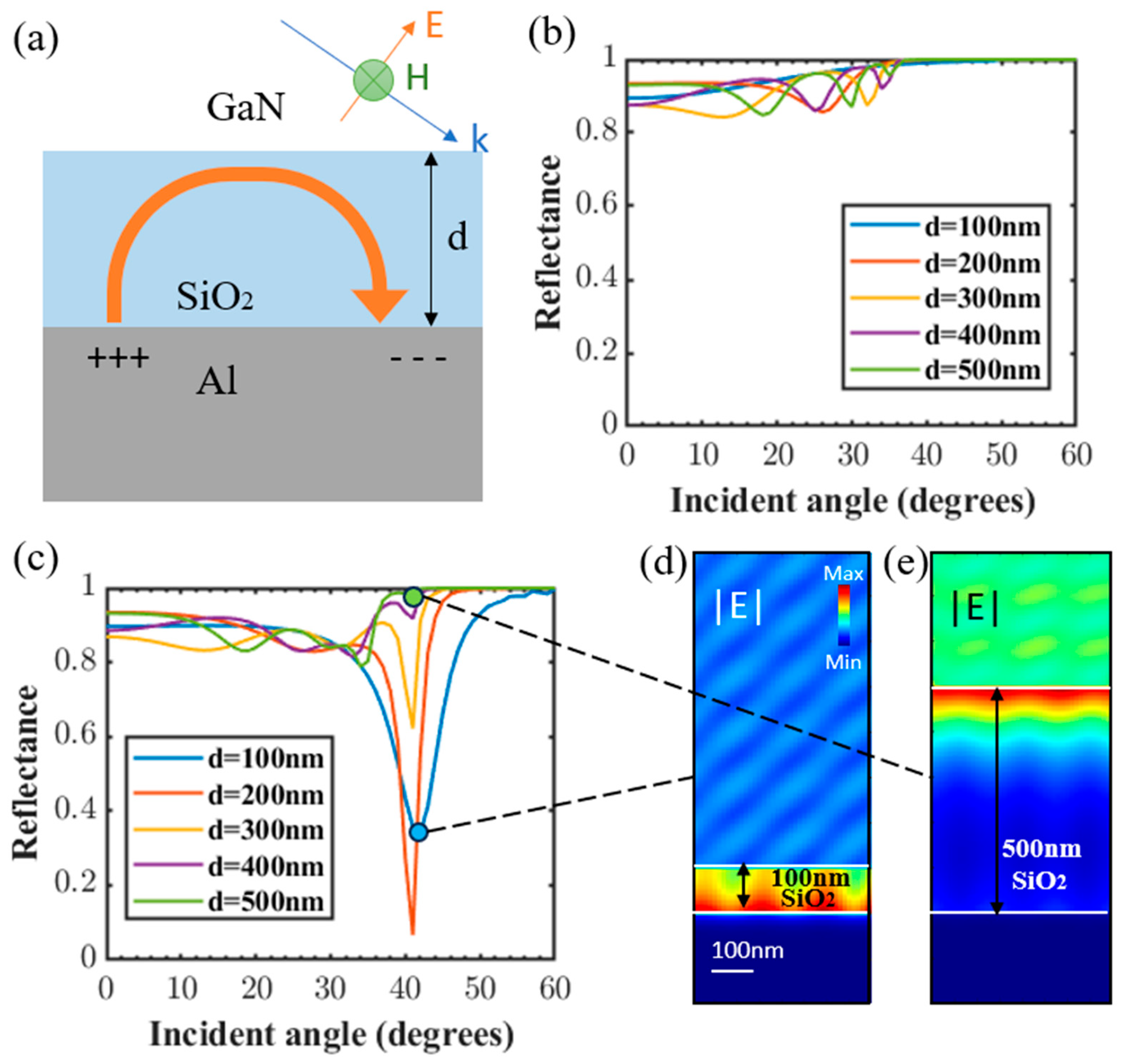
3.1. Reducing the Loss from Surface Plasmon

To recycle the bottom emitted light and to narrow the radiation patterns, a reflective sidewall composed of metals, such as Al and Ag, is typically applied in μLEDs with dielectric surface passivation. On the other hand, SPP modes may be excited on the metal–dielectric interface. Due to momentum matching conditions, surface plasmon resonance will be excited at a specific incident angle, which induces strong absorption loss [30,31]. Figure 3a describes the SPP mode inside the multi-layered GaN-SiO2-Al reflective structure. With a TM plane wave excitation, the SPP confined in the SiO2 layer travels along the metal–dielectric interface, introducing a nonradiative loss originating from the damping of excited electrons in the metal at the resonance frequency. Figure 3b,c show the FDTD-calculated reflectance of the multi-layer Al reflector with different SiO2 dielectric layer thickness as a function of the incident angle for the TE and TM plane waves, respectively. For the TE incidence, the SPP mode is forbidden because of lacking an electric field along the wave propagation direction, and the minor absorption loss mostly comes from the material. However, a reflectance dip at around 40° is found for the TM light incidence, especially when the dielectric layer thickness is below 400 nm. As the passivate dielectric layer thickness increases to 400 nm, the reflectance increases to over 80% in the whole spectra, and the loss from SPP resonance is suppressed. To investigate the underlying mechanisms behind the far-field reflectance response for the dielectric-coated metallic reflector, we calculated the near-field distribution profile of the electric field amplitude. Figure 3d reveals that an intense electric field is localized at the metal–dielectric interface and confined by the 100 nm thin SiO2 layer. For the light incident from GaN into SiO2, the total internal reflection (TIR) condition is reached when the incident angle exceeds 36.8°. Therefore, SPP is excited by the evanescent wave from TIR in this case since the dielectric layer is very thin. On the other hand, Figure 3e shows that the evanescent wave can barely reach the metal–dielectric interface, and an almost unity reflectance can be achieved due to the thick SiO2 layer. Instead, an intense electric field is only localized at the GaN/SiO2 interface. Overall, a passivate dielectric thickness over 400 nm is necessary to suppress SPP mode and obtain a high reflectance for the Al reflectors.

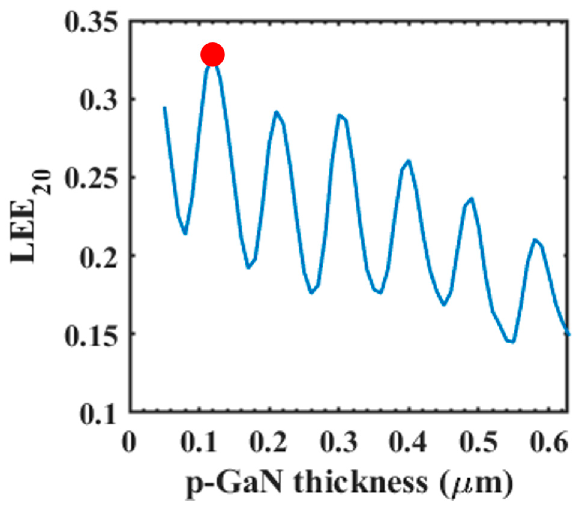
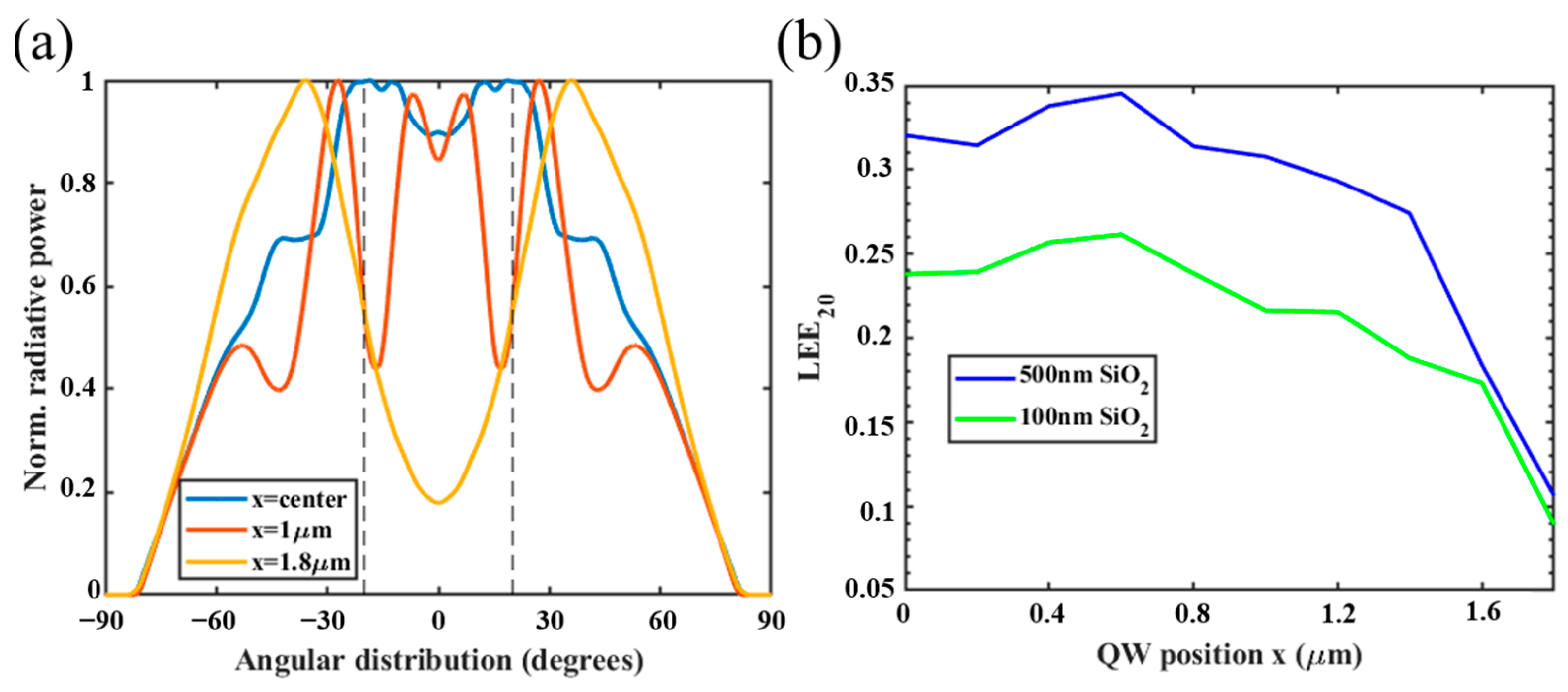
3.2. μLED Optical Performance

In the vertical-chip cylindrical µLED with a metallic sidewall, as shown in Figure 1, the LEE is mainly dependent on the following three factors: (1) the focus of CPC structure, (2) the reflectance from Al sidewall, and (3) the TIR inside the GaN chip. Therefore, to maximize LEE, proper p-GaN layer thickness is required [32]. Limited by computer memories, we only consider the electric dipoles in the center of the active region to simulate the optical properties of the SQW because the CPC structure can efficiently concentrate light through its focal point [26]. As shown in Figure 4, by sweeping the p-GaN thickness from 0.05 μm to 0.64 μm, the optimized effective LEE is found to be 32.5% when the p-GaN thickness is 0.12 μm.
After determining the optimized p-GaN thickness, we calculate the position-dependent angular distribution of the selected dipoles, as shown in Figure 5a. For dipoles placed at the center of the quantum well, the emission is more directional because it is closer to the CPC focal point. On the other hand, the angular distribution of dipoles which are close to the edge of the quantum well (e.g., x = 1.8 μm) is much broader. In addition, the batwing profile might induce angular color shift [33]. Therefore, as depicted in Figure 5b, the effective LEE decreases as the dipole moves closer to the edge of the quantum well. Due to interference, the effective LEE slightly fluctuates with the dipole position, which can also be found in previous studies [25]. As a result, the light out-coupling of dipoles at the edge of the quantum well is less efficient than those dipoles in the center.

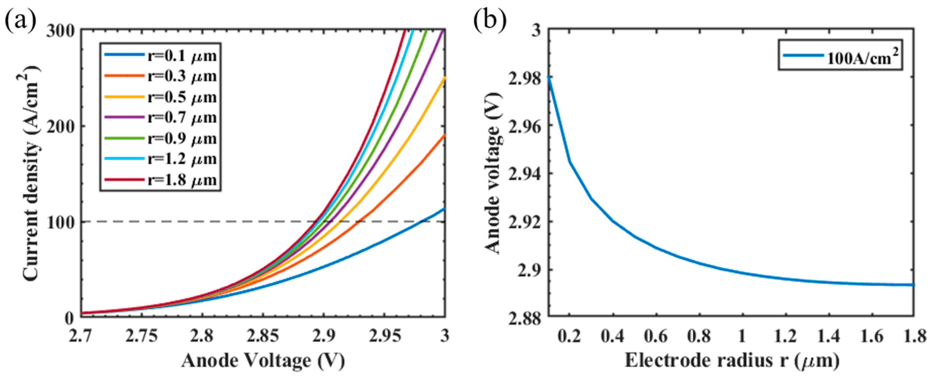
3.3. µLED Electrical Performance

Based on the parameters in Section 2.3, the I–V curve is calculated, and the results are plotted in Figure 6a. As the p-contact radius (r) decreases from 1.8 μm to 0.1 μm, the slope of the I–V curve keeps decreasing. That means, for the same operating current density (e.g., 100 A/cm2; the horizontal dashed lines), the μLED with a smaller p-contact requires a higher anode voltage because of less current diffusion. In this case, electrons will be confined in the center of the QW, and the effective cross-section of the QW is reduced. This phenomenon is more pronounced for an extremely small p-contact, and a similar trend is also found in Hsu’s previous work [34]. Figure 6b depicts that the required anode voltage to provide a current density of 100 A/cm2 slightly increases from ~2.895 V to ~2.980 V as r decreases from 1.8 μm to 0.1 μm. Thus, the μLED driving becomes more difficult as the p-contact radius decreases.
The normalized radiative recombination rate distribution in the QW is shown in Figure 7. For μLEDs with a small electrode, due to the thin p-GaN layer, the center of the QW will be excited more strongly than those regions near the sidewall because of less current diffusion [24]. In this scenario, the μLED efficiency would be reduced due to a stronger Auger recombination if the current density is high enough. On the other hand, for μLEDs with a large electrode, the curve is almost flat due to current diffusion. In this case, the efficiency degradation due to a sidewall defect will be more pronounced because the dipoles close to the sidewall defect region will be excited [35]. To include this part in our model, the IQE degradation on the μLED sidewall needs to be considered.

3.4. EQE Improvement

Based on the above analysis, for the CPC μLED with a reflective sidewall, the radiative recombination distribution of the QW is dependent on the p-GaN contact size. For a large radius p-contact, the current is more uniformly distributed, and the dipoles near the sidewall are more heavily excited, so that its driving voltage is lower. However, the dipoles on the edge suffer a stronger recombination loss due to sidewall defects. In addition, the effective LEE is lower for these dipoles. On the contrary, for a small radius p-contact, the dipoles placed in the center of the QW are more heavily excited, which helps reduce the sidewall effect. However, the Auger recombination loss can be more significant, depending on the operating current density [36].
The IQE degradation due to sidewall damage can be visualized by the cathodoluminescence (CL) lifetime measurement of the SQW. According to Finot’s work [37], if we consider that the IQE in the center of the active layer is 100%, the IQE decreases from 1 to ~0.6 due to sidewall damage (Figure 8 inset). By considering all the factors, Figure 8 indicates that the highest EQE of 17.8% is achieved when the electrode radius is r = 0.1 μm at 100 A/cm2 operating current. By increasing d from 100 nm to 500 nm, when r = 1.8 μm, the EQE increases from 11.7% to 15.4%, corresponding to a 31.6% improvement. When d = 500 nm (the blue line in Figure 8), EQE increases from 15.4% to 17.8% by reducing the p-contact radius from 1.8 μm to 0.1 μm, which corresponds to another 15.6% improvement. Therefore, the overall EQE improvement is 52.1%. However, a minor tradeoff is that the operating voltage increases from 2.895 V to 2.980 V, which can lead to a slightly heavier load to the driving backplane.

4. Conclusions

We have analyzed and optimized the blue InGaN/GaN CPC μLED with Al sidewall by implementing both an electrical model in TCAD and optical model in FDTD. First, via 2D-FDTD simulation, we adjust the passivation layer thickness on Al to achieve a higher reflectance by forbidding the SPP mode. Afterward, a dipole cloud model is employed to calculate the optical response of the CPC µLED. For parabolic µLEDs with metallic sidewalls, the light generated at the center of the active layer couples out more easily compared to that generated at the edge. In addition, dipoles close to the sidewall of the chip suffer from a lower IQE due to sidewall damage. To reduce the electrical weighting of edge dipoles, an electrical model in TCAD is applied to control the current distribution by varying the electrode size, and a 15.6% EQE improvement is achieved. By further optimizing LEE through p-GaN thickness and considering the sidewall reflectance by optimizing SiO2 thickness, a total of 52.1% EQE improvement is obtained. The EQE after optimization is 17.8%. Such an optimized structure will help micro-LEDs to achieve higher efficiency for TVs, AR glasses, and automotive displays.

Author Contributions

Methodology, Y.Q., E.-L.H., Y.-H.H. and K.-H.L.; simulations, Y.Q.; writing—original draft preparation, Y.Q.; writing—review and editing, S.-T.W.; supervision, S.-T.W. All authors have read and agreed to the published version of the manuscript.

Funding

This research is supported by the AUO Corporation.

Data Availability Statement

The data presented in this study are available from the authors upon reasonable request.

Conflicts of Interest

The authors declare that this study received funding from the AUO Corporation. The funder was not involved in the study design, collection, analysis, interpretation of data, the writing of this article or the decision to submit it for publication.

References

  1. Biwa, G.; Aoyagi, A.; Doi, M.; Tomoda, K.; Yasuda, A.; Kadota, H. Technologies for the Crystal LED display system. J. Soc. Inf. Disp. 2021, 29, 435–445. [Google Scholar] [CrossRef]
  2. Huang, Y.; Hsiang, E.-L.; Deng, M.-Y.; Wu, S.-T. Mini-LED, Micro-LED and OLED displays: Present status and future perspectives. Light Sci. Appl. 2020, 9, 105. [Google Scholar] [CrossRef] [PubMed]
  3. Miao, W.C.; Hsiao, F.H.; Sheng, Y.; Lee, T.Y.; Hong, Y.H.; Tsai, C.W.; Chen, H.L.; Liu, Z.; Lin, C.L.; Chung, R.J. Microdisplays: Mini-LED, Micro-OLED, and Micro-LED. Adv. Opt. Mater. 2023, 12, 2300112. [Google Scholar] [CrossRef]
  4. Lin, C.-C.; Wu, Y.-R.; Kuo, H.-C.; Wong, M.S.; DenBaars, S.P.; Nakamura, S.; Pandey, A.; Mi, Z.; Tian, P.; Ohkawa, K.; et al. The micro-LED roadmap: Status quo and prospects. J. Phys. Photonics 2023, 5, 042502. [Google Scholar] [CrossRef]
  5. Chen, Z.; Yan, S.; Danesh, C. MicroLED technologies and applications: Characteristics, fabrication, progress, and challenges. J. Phys. D Appl. Phys. 2021, 54, 123001. [Google Scholar] [CrossRef]
  6. Lin, J.; Jiang, H. Development of microLED. Appl. Phys. Lett. 2020, 116, 100502. [Google Scholar] [CrossRef]
  7. Liu, Z.; Lin, C.-H.; Hyun, B.-R.; Sher, C.-W.; Lv, Z.; Luo, B.; Jiang, F.; Wu, T.; Ho, C.-H.; Kuo, H.-C. Micro-light-emitting diodes with quantum dots in display technology. Light Sci. Appl. 2020, 9, 83. [Google Scholar] [CrossRef] [PubMed]
  8. Anwar, A.R.; Sajjad, M.T.; Johar, M.A.; Hernández-Gutiérrez, C.A.; Usman, M.; Łepkowski, S. Recent progress in micro-LED-based display technologies. Laser Photonics Rev. 2022, 16, 2100427. [Google Scholar] [CrossRef]
  9. Zhou, X.; Tian, P.; Sher, C.-W.; Wu, J.; Liu, H.; Liu, R.; Kuo, H.-C. Growth, transfer printing and colour conversion techniques towards full-colour micro-LED display. Prog. Quant. Electron. 2020, 71, 100263. [Google Scholar] [CrossRef]
  10. Wu, Y.; Ma, J.; Su, P.; Zhang, L.; Xia, B. Full-color realization of micro-LED displays. Nanomaterials 2020, 10, 2482. [Google Scholar] [CrossRef]
  11. Qian, Y.; Yang, Z.; Hsiang, E.-L.; Yang, Q.; Nilsen, K.; Huang, Y.-H.; Lin, K.-H.; Wu, S.-T. Human Eye Contrast Sensitivity to Vehicle Displays under Strong Ambient Light. Crystals 2023, 13, 1384. [Google Scholar] [CrossRef]
  12. Hsiang, E.-L.; Yang, Z.; Yang, Q.; Lai, P.-C.; Lin, C.-L.; Wu, S.-T. AR/VR light engines: Perspectives and challenges. Adv. Opt. Photonics 2022, 14, 783–861. [Google Scholar] [CrossRef]
  13. Olivier, F.; Tirano, S.; Dupré, L.; Aventurier, B.; Largeron, C.; Templier, F. Influence of size-reduction on the performances of GaN-based micro-LEDs for display application. J. Lumin. 2017, 191, 112–116. [Google Scholar] [CrossRef]
  14. Boussadi, Y.; Rochat, N.; Barnes, J.-P.; Bakir, B.B.; Ferrandis, P.; Masenelli, B.; Licitra, C. Investigation of sidewall damage induced by reactive ion etching on AlGaInP MESA for micro-LED application. J. Lumin. 2021, 234, 117937. [Google Scholar] [CrossRef]
  15. Olivier, F.; Daami, A.; Licitra, C.; Templier, F. Shockley-Read-Hall and Auger non-radiative recombination in GaN based LEDs: A size effect study. Appl. Phys. Lett. 2017, 111, 022104. [Google Scholar] [CrossRef]
  16. Smith, J.M.; Ley, R.; Wong, M.S.; Baek, Y.H.; Kang, J.H.; Kim, C.H.; Gordon, M.J.; Nakamura, S.; Speck, J.S.; DenBaars, S.P. Comparison of size-dependent characteristics of blue and green InGaN microLEDs down to 1 μm in diameter. Appl. Phys. Lett. 2020, 116, 071102. [Google Scholar] [CrossRef]
  17. Ley, R.T.; Smith, J.M.; Wong, M.S.; Margalith, T.; Nakamura, S.; DenBaars, S.P.; Gordon, M.J. Revealing the importance of light extraction efficiency in InGaN/GaN microLEDs via chemical treatment and dielectric passivation. Appl. Phys. Lett. 2020, 116, 251104. [Google Scholar] [CrossRef]
  18. Yu, J.; Tao, T.; Liu, B.; Xu, F.; Zheng, Y.; Wang, X.; Sang, Y.; Yan, Y.; Xie, Z.; Liang, S. Investigations of sidewall passivation technology on the optical performance for smaller size GaN-based micro-LEDs. Crystals 2021, 11, 403. [Google Scholar] [CrossRef]
  19. Wong, M.S.; Kearns, J.A.; Lee, C.; Smith, J.M.; Lynsky, C.; Lheureux, G.; Choi, H.; Kim, J.; Kim, C.; Nakamura, S. Improved performance of AlGaInP red micro-light-emitting diodes with sidewall treatments. Opt. Express 2020, 28, 5787–5793. [Google Scholar] [CrossRef]
  20. Wong, M.S.; Lee, C.; Myers, D.J.; Hwang, D.; Kearns, J.A.; Li, T.; Speck, J.S.; Nakamura, S.; DenBaars, S.P. Size-independent peak efficiency of III-nitride micro-light-emitting-diodes using chemical treatment and sidewall passivation. Appl. Phys. Express 2019, 12, 097004. [Google Scholar] [CrossRef]
  21. Pandey, A.; Reddeppa, M.; Mi, Z. Recent progress on micro-LEDs. Light Adv. Manu. 2024, 4, 519–542. [Google Scholar] [CrossRef]
  22. Gilet, P.; Robin, I.-C. 52-1: Invited Paper: Nanostructures on Silicon to Solve the Active Display Paradigms. In SID Symposium Digest of Technical Papers; Wiley: Hoboken, NJ, USA, 2018; pp. 684–687. [Google Scholar]
  23. Pandey, A.; Xiao, Y.; Reddeppa, M.; Malhotra, Y.; Liu, J.; Min, J.; Wu, Y.; Mi, Z. A red-emitting micrometer scale LED with external quantum efficiency> 8%. Appl. Phys. Lett. 2023, 122, 151103. [Google Scholar] [CrossRef]
  24. Behrman, K.; Kymissis, I. Enhanced microLED efficiency via strategic pGaN contact geometries. Opt. Express 2021, 29, 14841–14852. [Google Scholar] [CrossRef] [PubMed]
  25. Qian, Y.; Yang, Z.; Huang, Y.-H.; Lin, K.-H.; Wu, S.-T. Directional high-efficiency nanowire LEDs with reduced angular color shift for AR and VR displays. Opto-Electron. Sci. 2022, 1, 220021. [Google Scholar] [CrossRef]
  26. Hsiang, E.-L.; He, Z.; Yang, Z.; Lan, Y.-F.; Wu, S.-T. Tailoring the light distribution of micro-LED displays with a compact compound parabolic concentrator and an engineered diffusor. Opt. Express 2021, 29, 39859–39873. [Google Scholar] [CrossRef] [PubMed]
  27. Liu, Z.; Wang, K.; Luo, X.; Liu, S. Precise optical modeling of blue light-emitting diodes by Monte Carlo ray-tracing. Opt. Express 2010, 18, 9398–9412. [Google Scholar] [CrossRef]
  28. Konig, T.A.; Ledin, P.A.; Kerszulis, J.; Mahmoud, M.A.; El-Sayed, M.A.; Reynolds, J.R.; Tsukruk, V.V. Electrically tunable plasmonic behavior of nanocube–polymer nanomaterials induced by a redox-active electrochromic polymer. ACS Nano 2014, 8, 6182–6192. [Google Scholar] [CrossRef] [PubMed]
  29. Ryu, H.; Jeon, K.; Kang, M.; Yuh, H.; Choi, Y.; Lee, J. A comparative study of efficiency droop and internal electric field for InGaN blue lighting-emitting diodes on silicon and sapphire substrates. Sci. Rep. 2017, 7, 44814. [Google Scholar] [CrossRef] [PubMed]
  30. Maier, S.A. Plasmonics: Fundamentals and Applications; Springer: Berlin/Heidelberg, Germany, 2007. [Google Scholar]
  31. Pitarke, J.; Silkin, V.; Chulkov, E.; Echenique, P. Theory of surface plasmons and surface-plasmon polaritons. Rep. Prog. Phys. 2006, 70, 1–87. [Google Scholar] [CrossRef]
  32. Wang, L.; Sun, J.; Yan, Q.; Lin, J.; Guo, W.; Chen, E.; Xu, C.; Liu, Y. Issue of spatial coherence in MQW based micro-LED simulation. Opt. Express 2021, 29, 31520–31526. [Google Scholar] [CrossRef]
  33. Gou, F.; Hsiang, E.-L.; Tan, G.; Chou, P.-T.; Li, Y.-H.; Lan, Y.-F.; Wu, S.-T. Angular color shift of micro-LED displays. Opt. Express 2019, 12, A746–A757. [Google Scholar] [CrossRef] [PubMed]
  34. Hsu, Y.-H.; Lin, Y.-H.; Wu, M.-H.; Kuo, H.C.; Horng, R.-H. Current Confinement Effect on the Performance of Blue Light Micro-LEDs with 10 μm Dimension. ACS Omega 2023, 8, 35351–35358. [Google Scholar] [CrossRef] [PubMed]
  35. Wu, Z.; Ren, K.; Zhang, X.; An, Y.; Yin, L.; Lu, X.; Guo, A.; Zhang, J. Physical mechanisms on the size-effect in GaN-based Micro-LEDs. Micro Nanostruct. 2023, 177, 207542. [Google Scholar] [CrossRef]
  36. Hang, S.; Zhang, G.; Chu, C.; Zhang, Y.; Zheng, Q.; Li, Q.; Zhang, Z.-H. On the impact of the beveled mesa for GaN-based micro-light emitting diodes: Electrical and optical properties. Opt. Express 2022, 30, 37675–37685. [Google Scholar] [CrossRef]
  37. Finot, S.; Le Maoult, C.; Gheeraert, E.; Vaufrey, D.; Jacopin, G. Surface recombinations in III-nitride micro-LEDs probed by photon-correlation cathodoluminescence. ACS Photonics 2021, 9, 173–178. [Google Scholar] [CrossRef]
Figure 1. Geometry of µLED and schematic of 2D FDTD simulation model in xy plane.
Crystals 14 00503 g001
Figure 2. Electrical simulation model validation through I–V curve fitting with experimental data.
Crystals 14 00503 g002
Figure 3. (a) SPP excitation on Al-SiO2-GaN multi-layer structure. (b,c) FDTD-calculated reflectance spectra for the Al reflector with different SiO2 thickness excited by (b) TE and (c) TM incidence, respectively. (d,e) FDTD-calculated distribution maps of |E| at SPP mode when (d) d = 100 nm and (e) d = 500 nm, respectively.
Crystals 14 00503 g003
Figure 4. FDTD-calculated effective LEE as a function of p-GaN thickness. Red dot indicates the optimized effective LEE when p-GaN thickness is 0.12 μm.
Crystals 14 00503 g004
Figure 5. (a) Simulated radiation pattern of the center dipole (blue) and other selected dipoles whose distance from the center of the quantum well is 1 μm (orange) and 1.8 μm (yellow). (b) Simulated effective LEE as a function of the distance from the dipole to the center of the quantum well when dielectric coating is 500 nm (blue) and 100 nm (green).
Crystals 14 00503 g005
Figure 6. (a) Simulated I–V characteristic curves with p-contact radius varying from 0.1 μm to 1.8 μm. (b) The corresponding anode voltage at current density = 100 A/cm2.
Crystals 14 00503 g006
Figure 7. TCAD-calculated normalized radiative recombination rate distribution in the QW with a varying r.
Crystals 14 00503 g007
Figure 8. Effective EQE by varying p-contact radius from 0.1 μm to 1.8 μm. Inset: IQE degradation due to sidewall defect.
Crystals 14 00503 g008
Table 1. Material, thickness, and doping concentration of the μLED in Silvaco TCAD simulation.
MaterialThicknessDoping
Au100 nmN/A
pGaN120 nm1 × 1020/cm3
pAlGaN50 nm1 × 1020/cm3
InGaN3 nmN/A
nGaN2.83 μm1 × 1020/cm3
ITO100 nmN/A
Disclaimer/Publisher’s Note: The statements, opinions and data contained in all publications are solely those of the individual author(s) and contributor(s) and not of MDPI and/or the editor(s). MDPI and/or the editor(s) disclaim responsibility for any injury to people or property resulting from any ideas, methods, instructions or products referred to in the content.

