Article

Tailoring the Graphene Properties for Electronics by Dielectric Materials

by
Isaac Appiah Otoo
1,
Aleksandr Saushin
1,
Seth Owusu
1,
Petri Karvinen
1,
Sari Suvanto
2,
Yuri Svirko
1,
Polina Kuzhir
1 and
Georgy Fedorov
1,*
1
Department of Physics and Mathematics, University of Eastern Finland, FI-80100 Joensuu, Finland
2
Department of Chemistry, University of Eastern Finland, FI-80100 Joensuu, Finland
*
Author to whom correspondence should be addressed.
Crystals 2024, 14(7), 595; https://doi.org/10.3390/cryst14070595
Submission received: 3 June 2024 / Revised: 18 June 2024 / Accepted: 23 June 2024 / Published: 27 June 2024
(This article belongs to the Special Issue Advanced Technologies in Graphene-Based Materials)

Abstract

:
Tunability of properties is one of the most important features of 2D materials, among which graphene is attracting the most attention due to wide variety of its possible applications. Here, we demonstrated that the carrier concentration in graphene can be efficiently tuned by the material of the dielectric substrate on which it resides. To this end, we fabricated samples of CVD-grown graphene transferred onto silicon wafers covered with alumina, titanium dioxide, and silicon dioxide. We measured the transmission spectra of these samples using a time-domain terahertz spectrometer and extracted the Drude frequency-dependent graphene conductivity. We found that the sheet resistance of graphene is strongly affected by the underlying dielectric material, while the carrier scattering time remains the same. The carrier concentration value was found to range from 7 × 10 11 / c m 2 in the case of alumina and 4.5 × 10 12 / c m 2 in the case of titanium dioxide. These estimations are consistent with what can be extracted from the position of the G-peak in the Raman spectra of graphene. Our results show a way to control the graphene doping level in applications where it does not have to be adjusted.

1. Introduction

Graphene has attracted a lot of attention during the last decades because of its unique electronic properties giving it enormous potential [1]. The everlasting interest graphene has received is due to its remarkable electrical, mechanical, and optical properties [2] that have a large promise for numerous applications [3,4,5,6,7]. These include an enormous thermal conductivity [8] (up to 5 × 10³ W/mK in the ref. [9]), high mobility of electrons (2 × 105 cm2 V−1 s−1 [10]), and ability to absorb 2.3% of incident radiation in a wide spectral range spanning from infrared to ultraviolet [6].
These properties of graphene are mainly governed by the concentration of charge carriers that can be controlled via electrostatic [11] or chemical [12] doping. Correspondingly, varying the carrier’s concentration by electrostatic doping allows one to control its conductivity and absorptivity and to create graphene-based transistors [13], plasmonic interferometers [14], optical switches [15], and other optoelectronic devices. However, applications such as chemical sensing [16] often require graphene to be doped to a certain constant level. This can be achieved either by exploring electrostatic doping by adding a gate electrode to the device architecture or by chemical doping via graphene functionalization. The former approach essentially complicates the fabrication process, while the latter one introduces extra defects that may affect sensor performance.
It is known that underlying dielectric substrates are capable of providing constant doping of deposited graphene and carbon nanotubes [17,18]. However, the origin of this effect is still unknown. Recent work [19] reported on the substrate effect on the THz dynamic conductivity of graphene transferred onto bare silicon, silicon coated with Si3N4 and silicon coated with SiO2. The graphene layer electromagnetic response was described within the Drude model and the DC surface conductivity as well as the scattering time were estimated based on the transmission spectra of the graphene-coated substrate. It has been shown that both the carrier scattering time and concentration depend on the substrate material. This approach allows for the non-invasive characterization of graphene’s transport properties. The methodology of graphene AC conductivity reconstruction developed in [19] relies on the assumption that the THz response of graphene is not dependent on the THz dispersion of the used dielectric substrate, which leads to substantial blurring of the conductivity values reconstructed from the experimental data.
In this paper, we extended the approach developed in ref. [19] to show that the properties of the charge carriers in graphene can be efficiently tuned by the material of the dielectric substrate on which it resides. For this work, we have chosen three different dielectric substrates with thicknesses ensuring good Raman signals [20] in order to estimate the graphene doping level based on its Raman spectra [21]. Using THz time-domain spectroscopy (TTDS), we measured the transmission spectra of graphene deposited on a silicon wafer coated with SiO2, TiO2, or Al2O3. We compared the transmission spectra of the substrate with and without graphene and used the transfer matrix technique [22] to obtain the DC sheet resistance and the carrier scattering time of the graphene layer. We further improved this simple and nondestructive methodology of measuring the AC conductivity of supported graphene via THz transmission data analysis. We considered consistently the contribution of the substrate as is, and then reconstructed the constitutive parameters of the supported graphene from the THz spectra. It decreased the measurement error down to less than 20%. We thus achieved an estimation of the carrier concentration with an accuracy that is much better than that in ref [19]. Our results confirmed that the THz conductivity of graphene can be well described by the Drude model and allowed us to obtain the DC conductance and scattering time in our graphene samples. Using this improved methodology, we obtained an important result, i.e., we demonstrated that the scattering time is not sensitive to the substrate, indicating that the carrier’s mean free path is determined by the defects introduced during the graphene synthesis and transfer rather than the substrate material. On the other hand, the DC sheet resistance varied from 350 Ω/sq for graphene deposited on TiO2 to 900 Ω/sq for graphene deposited on Al2O3. The graphene carrier concentration varied from 7 × 10 11 / c m 2 on the alumina substrate to 4.5 × 10 12 / c m 2 on the titanium dioxide substrate. These estimations are consistent with those of the position of the G-peak in the Raman spectra of graphene [21]. We believe that our results provide an opportunity to achieve a constant concentration of the charge carriers in graphene without electrostatic and/or chemical doping.
The collected data of graphene doping due to the presence of conventional substrates are in good agreement with those measured via Raman scattering and give even less scattered results than those provided by the Raman technique. This approach allows for treating the developed THz spectroscopy method of determining the carrier concentrations and AC conductivity of supported graphene as a future standard methodology to support graphene characterization. Moreover, through the reconstruction of the doping level of supported graphene through its interaction with several dielectric substrates, we found the most conductive and less defective samples, i.e., graphene supported by Al2O3 and TiO2.

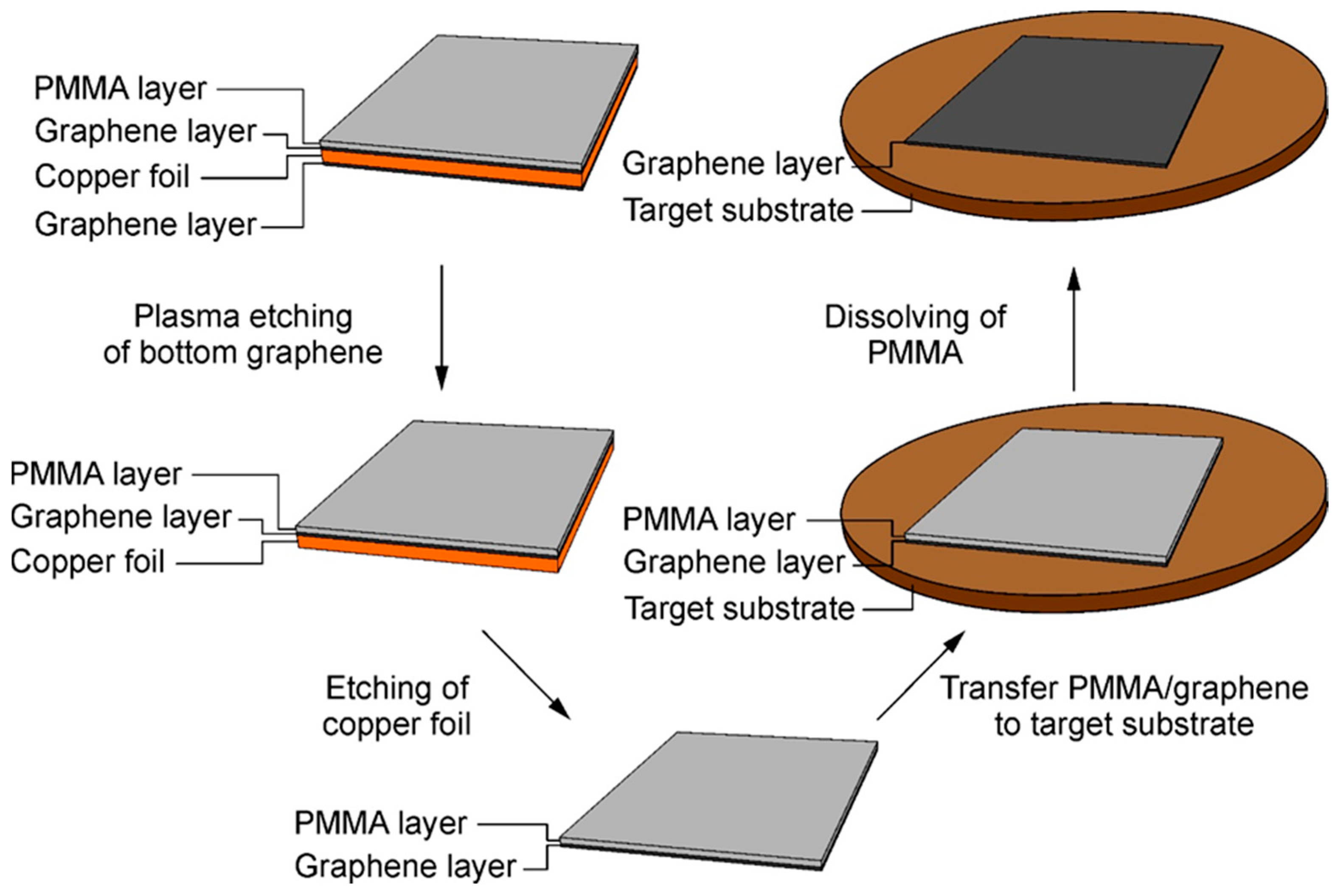
2. Materials and Methods

In these experiments, we used commercial graphene samples (Graphenea) synthesized on copper foil using the chemical vapor deposition (CVD) method and covered with a 65 nm layer of poly-methyl methacrylate (PMMA) on one side (see Figure 1). Graphene was transferred onto silicon 275 μm wafers covered with a layer of Al2O3 (96 nm) or TiO2 (150 nm) using atomic layer deposition (ALD). Additionally, we used a commercially available silicon wafer covered with a 3 μm thick layer of thermally grown SiO2.
The transfer process started with etching graphene on the side of the copper foil not covered with PMMA using an Oxford Instruments PlasmaLab80 etcher. Then, to dissolve the copper foil and get the graphene ready for transferring, we left the copper with graphene overnight in an iron chloride (FeCl3) solution consisting of 90 g of FeCl3 and 200 mL deionized water. After that, we moved the graphene/PMMA layer to a beaker with deionized water to wash away the remains of the FeCl3 solution. Next, we transferred the graphene to another beaker with new deionized water five times. Then we transferred the graphene with PMMA on the target substrates and let it dry overnight. We next removed the PMMA layer by keeping it in acetone for 30 min and dried the sample under air for 5 min. After that, each sample was washed in isopropanol for 5 min, dried under air, washed in deionized water and dried one more time.
The samples were characterized by measuring their Raman spectra in the 1100 to 3500 cm−1 range by using 514 and 785 nm excitation wavelengths at 25 and 150 mW power, respectively.
As the main characterization technique, we employed transmission spectroscopy. The transmission of the samples in the THz range was studied with a time-domain spectrometer (TDS) (TeTechS, Waterloo, ON, Canada) based on a femtosecond laser with 795 nm in the transmission geometry with an aperture of 3 mm wavelength.

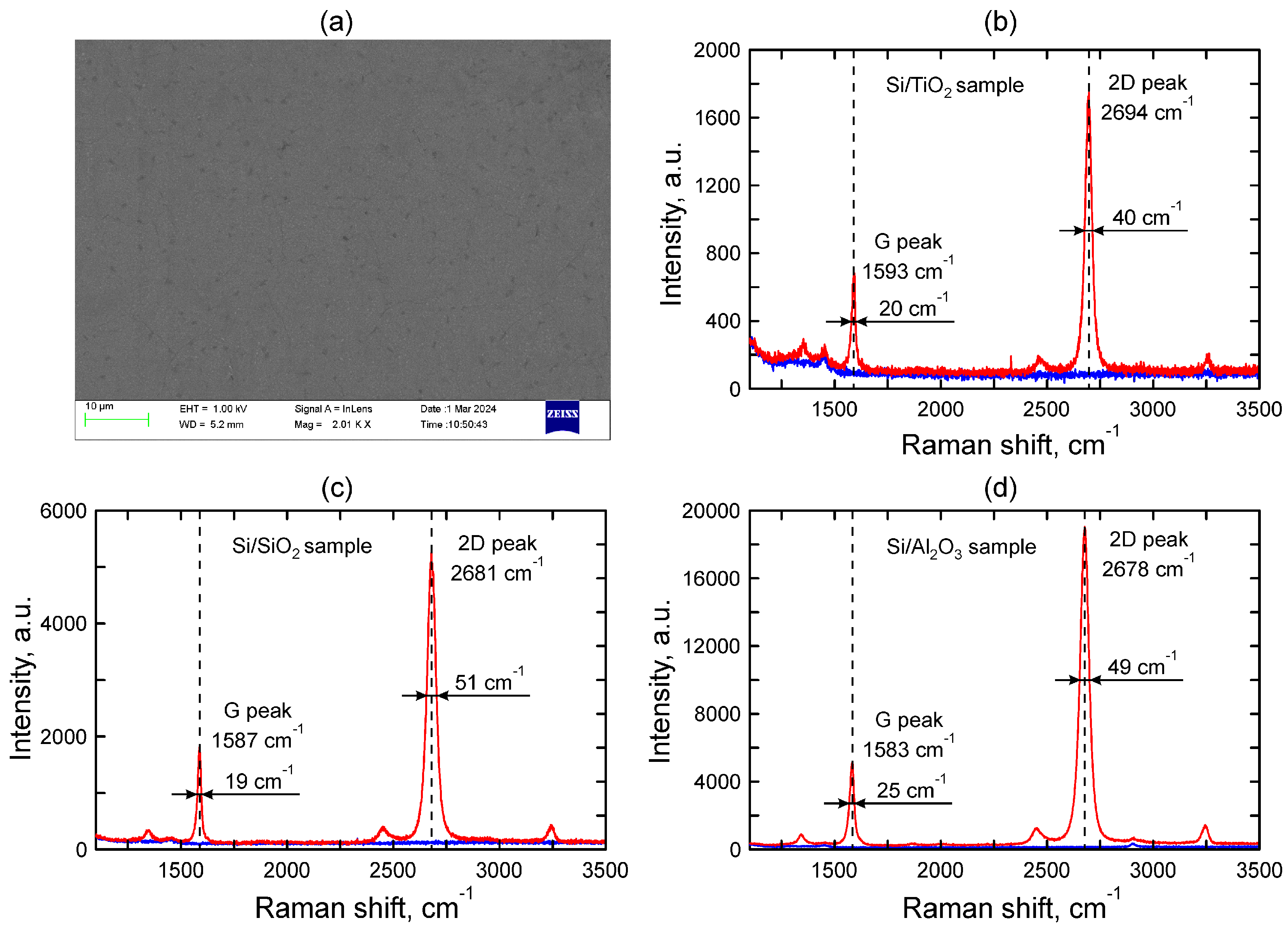
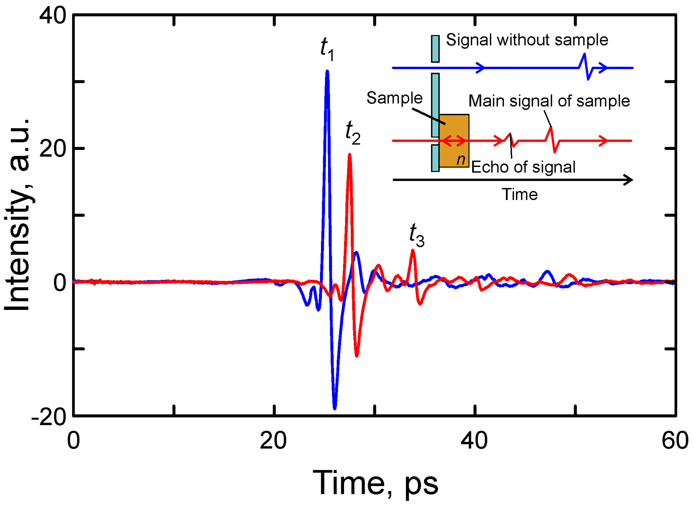
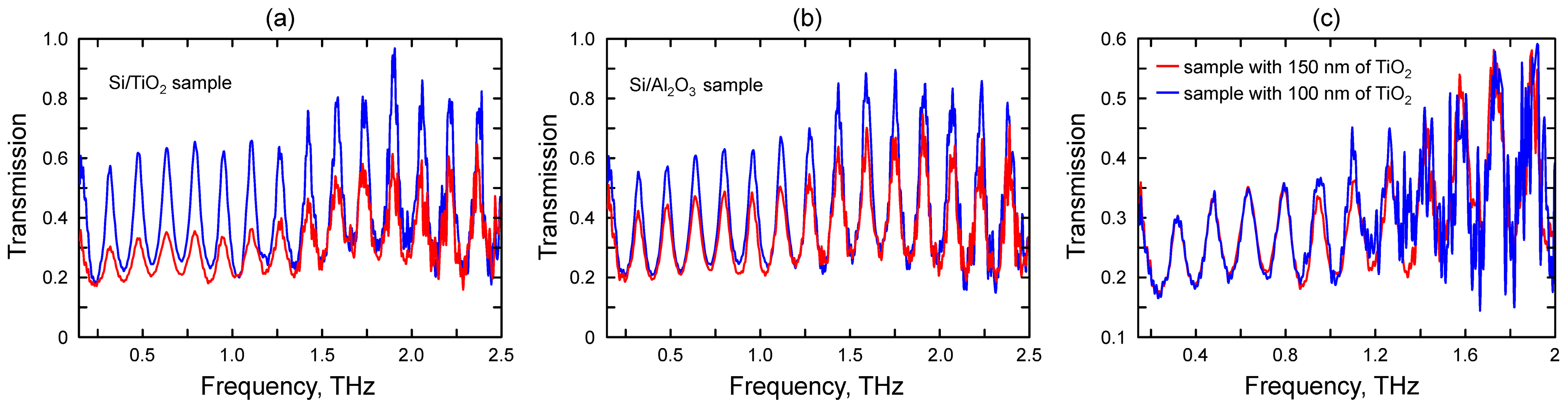
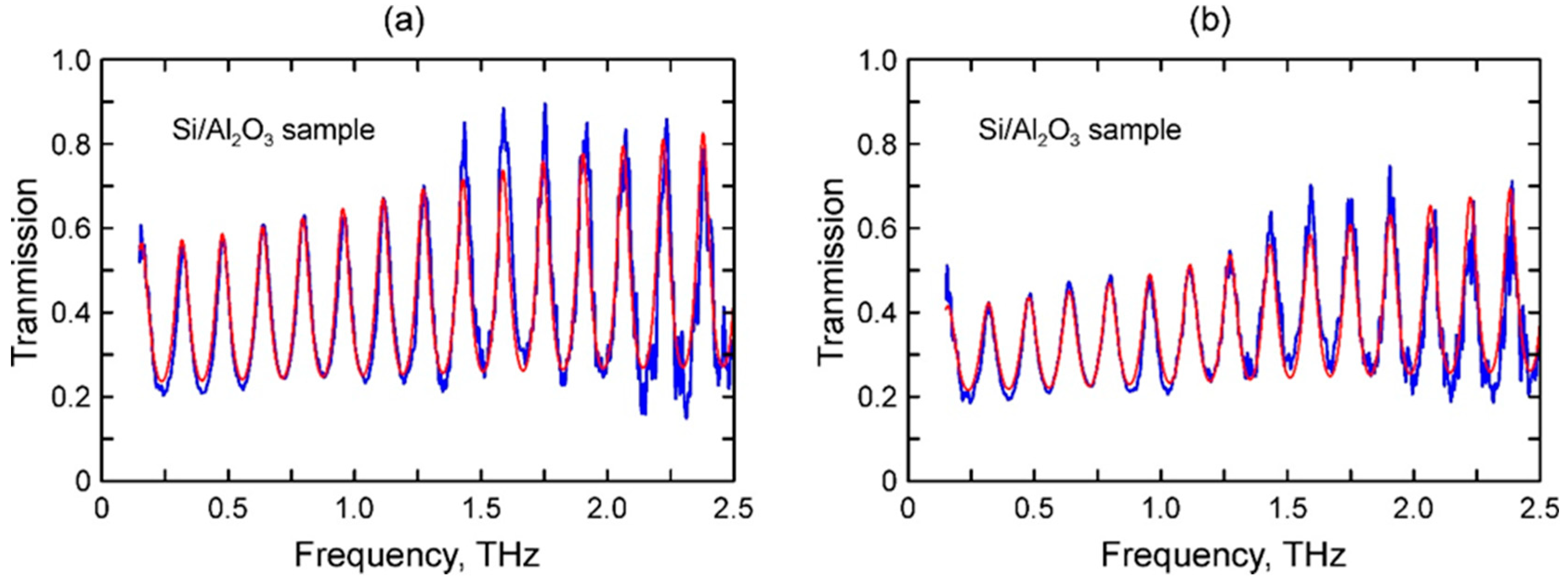
3. Results and Discussions

Figure 2a shows the SEM image of the graphene deposited onto a dielectric substrate. The Raman spectra of the TiO2, SiO2, and Al2O3 substrates (blue curves) with the graphene on them (red curves) are shown in Figure 2b–d, respectively. One can see that the SEM image is typical for graphene and that the spectra are dominated by D, G and 2D peaks. The D-peak lying around 1360 cm−1 is low in comparison with both the G and 2D peaks for each sample, which means that the graphene does not have a lot of defects. The intensity I2D of the 2D peak was more than two times that of the G peak (IG) for all samples. It is an indication of an unbent monolayer graphene. The exact peaks’ positions and I2D/IG ratios are presented in Table 1.
THz transmission spectroscopy allows one to measure the graphene surface conductivity (inverse of the sheet resistance) non-invasively [23], avoiding the lithography and metallization process required for the four-probe sheet resistance measurements. This approach was proven to be efficient in previous works. In our work, we used the transfer matrix method [22] and the Drude model for dynamic dielectric permittivity to analyze the measured spectra. We first fit the measured and simulated spectra for the bare substrate to extract the Drude parameters (DC conductivity and scattering time) of the silicon wafer and then used the same approach for graphene by fitting the corresponding spectra of graphene-coated substrates.
The thickness and refractive index of the silicon wafer were obtained from the time traces measured with the TDS. Figure 3 demonstrates typical time traces of the signal recorded in the case of an empty aperture (blue curve) and the case of a Si/TiO2 substrate. The time trace of the signal in the case of the Si/TiO2 substrate is delayed relative to the case of the empty aperture and has an additional echo because of reflections inside the substrate (see Figure 3, inset). Based on these two time traces we can calculate the refractive index n and thickness d c a l c of the substrates according to the following equations:
n = t 3 t 1 t 3 3 t 2 + 2 t 1 ,
d c a l c = c t 2 t 1 n 1 ,
where c is the speed of light in a vacuum and t 1 , t 2 and t 3 are illustrated in Figure 3. The results for all of the used substrates are summarized in Table 1. We note that the thicknesses of the silicon wafers we obtained using this method match the results of the direct measurements and the wafer thickness value provided by the producer. The calculated refractive indexes and thickness are presented in Table 2 along with the thicknesses dmeas measured with a micrometer and one can see that they approximately match.
The THz transmission spectra of the substrates covered with graphene and without it are illustrated in Figure 4a,b. The Fabri–Perot oscillations with a period depending on the substrate’s thickness and refractive index are seen in each graph. We also note that in the case of the bare substrate, transmittance tends to grow with frequency. This already indicates that the Drude scattering time is comparable with the inverse of the characteristic frequency. Transmission of the graphene-coated substrates is lower than that of the bare ones in all frequency ranges due to the intrinsic conductance of the graphene. Figure 4c shows the THz transmission spectra of the silicon substrates with 150 nm and 100 nm layers of TiO2. One can see that the spectra match well enough. This illustrates first the overall level of the reproducibility of the results. Secondly, it shows the lack of an effect of the dielectric layer thickness on the THz transmission spectra.
The propagation of the radiation through the sample can be described in terms of the transfer matrix method [22], which allows us to calculate the transmission, reflection, and absorption through a stack of parallel layers with known dielectric functions ε ω (the magnetic susceptibility is assumed to be the unit). The dielectric function of both the substrate and silicon are described within the Drude model, implying as follows:
ε ω = ε + 4 π i σ ω ω ,
σ ω = σ 0 1 i ω τ ,
where ω is the frequency of the incident THz radiation and σ0 is the DC conductivity σ(ω = 0). We first fit the transmission of the bare substrates using the silicon DC conductivity and scattering time as fitting parameters. Importantly, the silicon refractive index thickness is defined directly from the time traces. The scattering time turns out to be about 100 fs, consistent with previous studies [24], while the conductivity ranges from 10 to 30 S/m. Importantly the thickness of the ALD grown dielectric is much smaller that the radiation wavelength, so taking it into account does not affect the results of the simulations. This justifies considering the substrate as a uniform wafer with the thickness and refracted index evaluated based on the time traces. The same applies to the silica-on-silicon substrates. Next, we used the obtained dielectric function of the wafer and fit the transmission spectrum of the graphene-coated substrate to evaluate the sheet resistance Rsh = 1/σs and scattering for the graphene layer. In order to use Equations (3) and (4) for the graphene, we assume that the graphene sheet thickness is d = 0.35 nm. Still, the obtained value of the graphene sheet resistance does not depend on the graphene sheet thickness d, which is much smaller than both the wavelength and skin depth.
A comparison of the simulated and measured transmission spectra of the bare substrates is illustrated in Figure 5a and for the graphene-coated substrates in Figure 5b. The resulting characteristics of the graphene evaluated based on the transmission spectra are shown in Table 3.
The results obtained show that the sheet resistance of the graphene significantly depends on the substrate where it is placed. It varies from 350 Ω/sq for graphene on Si/TiO2 to 900 Ω/sq for graphene on Si/Al2O3 with an intermediate value of 550 Ω/sq for graphene on Si/SiO2. This allows us to suppose that the electronic properties of the substrate affect the Fermi level of the graphene due to the different levels of its doping. The scattering time of graphene derived from the calculated transmission spectra was about 80 ± 10 fs for all samples. Such a value corresponds to a mean free path of about 0.1 μm, which is typical for CVD-grown graphene [25]. The fact that the mean free path is the same for all graphene samples indicates that the concentration of defects does not depend on the substrate and is related only to the transfer of graphene and the CVD growth process. Correspondently, the difference in sheet resistance is determined mainly by the difference in the charge carriers’ concentration ns and we may describe its transport properties in terms of the semiclassical Boltzmann transport theory [26]. Since in our case EF >> kBT (degenerate Fermi gas), we may write an equation for the conductivity of 2D materials using the relaxation time calculated as follows:
σ S = e 2 υ f τ n s π ,
where σS = 1/Rsheet—sheet conductivity. Correspondingly,
n s = π 2 R s h e e t 2 e 4 υ f 2 τ 2 ,
where e = 1.6 × 10⁻¹⁹—electron charge, υf = 106 m/s—Fermi velocity. We found that ns = 4.5 × 1012 cm−2 for Si/TiO2, 1.8 × 1012 cm−2 for Si/SiO2 and 0.7 × 1012 cm−2 for Si/Al2O3.
It is informative to relate the graphene carrier concentration evaluated based on the transmission spectra to the Raman spectra of the corresponding samples. The graphene on the Si/TiO2 substrate had the highest charge concentration, and at the same time, its G and 2D peaks had the biggest Raman shift. The lowest Raman shifts were registered for graphene on Si/Al2O3, and the intermediate parameters belonged to graphene on the Si/SiO2 substrate; in other words, the greater the charge carrier’s concentration, the greater the Raman shifts of the G and 2D peaks. These results are consistent with the previous studies. According to [27], the charge concentration of graphene affects its Raman spectra. We used the results of ref [21] and the position of the G-peak in the measured Raman spectra to estimate the charge carrier concentration; see the last row of Table 1. The good match between the obtained concentration values provides solid ground for the reliability of our analysis. We note that the use of transmission spectroscopy allows for better accuracy in the evaluation of the carrier concentration, while the Raman data are used in our case for independent verification of these data.
Importantly, our data cannot be used to draw any conclusions on the carrier type. In other words, in no case can we tell whether graphene is p- or n- doped. Further studies will be needed to resolve this issue. Still, the absolute value of the charge carrier concentration is by itself a very important characteristic.

4. Conclusions

The dynamic charge transport of CVD graphene transferred onto Si/TiO2, Si/SiO2, and Si/Al2O3 substrates was investigated using time-domain terahertz range spectroscopy. Analysis of the transmission spectra unambiguously showed that graphene dynamic conductivity is well described by the Drude model with the DC surface conductance strongly dependent on the dielectric material in direct contact with the graphene. On the other hand, the carrier scattering time was found to be insensitive to it, meaning that the scattering time was limited by the intrinsic defects in the graphene and not by the substrate. Our data allow for a relatively accurate evaluation of carrier concentration. We found it to vary from 0.7 × 1012 cm−2 for graphene in contact with alumina to 4.5 × 1012 cm−2 for graphene in contact with titanium dioxide. These values are consistent with the carrier concentration estimations based on the positions of the G and 2D peaks of the measured Raman spectra.
We thus demonstrated that the graphene doping level can be efficiently engineered by choosing an appropriate substrate without a significant effect on the graphene quality (the mean free path). This approach may facilitate graphene applications for sensing and optoelectronic applications. The described methodology of the transmission spectra analysis may be extrapolated to use time-domain terahertz spectroscopy as a versatile tool for the characterization of 2D materials and thin films supported by silicon-based substrates.

Author Contributions

I.A.O. and P.K. (Petri Karvinen) fabricated the samples; A.S. and S.O. conducted the TDS measurements; S.S. measured the Raman spectra and analyzed the results; and G.F., P.K. (Polina Kuzhir) and Y.S. supervised the project and wrote the manuscript, with crucial contributions from all authors. All authors have read and agreed to the published version of the manuscript.

Funding

This study was accomplished with the financial support of subproject H-Cube of EU ATTRACT phase 2 Research infrastructure H2020 (Project No 101004462); the work is part of the Research Council of Finland Flagship Program, Photonics Research and Innovation (PREIN), decision number 346518; authors also acknowledge support of the Horizon 2020 RISE TERASSE Project (Project No 823878) and Research Council of Finland project (decision number 343393).

Data Availability Statement

The data that support the findings of this study are available from the corresponding authors upon reasonable request.

Conflicts of Interest

The authors declare no conflicts of interest.

References

  1. Geim, A.K. Graphene: Status and Prospects. Science 2009, 324, 1530–1534. [Google Scholar] [CrossRef]
  2. Castriota, M.; Politano, G.G.; Vena, C.; De Santo, M.P.; Desiderio, G.; Davoli, M.; Cazzanelli, E.; Versace, C. Variable Angle Spectroscopic Ellipsometry investigation of CVD-grown monolayer graphene. Appl. Surf. Sci. 2019, 467–468, 213–220. [Google Scholar] [CrossRef]
  3. Xia, Y.; Gao, W.; Gao, C. A Review on Graphene-Based Electromagnetic Functional Materials: Electromagnetic Wave Shielding and Absorption. Adv. Funct. Mater. 2022, 32, 2204591. [Google Scholar] [CrossRef]
  4. Lin, C.-H.; Chen, Y.-S.; Lin, J.-T.; Wu, H.C.; Kuo, H.-T.; Lin, C.-F.; Chen, P.; Wu, P.C. Automatic Inverse Design of High-Performance Beam-Steering Metasurfaces via Genetic-type Tree Optimization. Nano Lett. 2021, 21, 4981–4989. [Google Scholar] [CrossRef]
  5. Liao, C.; Li, Y.; Tjong, S.C. Graphene Nanomaterials: Synthesis, Biocompatibility, and Cytotoxicity. Int. J. Mol. Sci. 2018, 19, 3564. [Google Scholar] [CrossRef]
  6. Nair, R.R.; Blake, P.; Grigorenko, A.N.; Novoselov, K.S.; Booth, T.J.; Stauber, T.; Peres, N.M.R.; Geim, A.K. Fine Structure Constant Defines Visual Transparency of Graphene. Science 2008, 320, 1308. [Google Scholar] [CrossRef]
  7. Narayan, J.; Bezborah, K. Author response for “Recent advances in the functionalization, substitutional doping and applications of graphene/graphene composite nanomaterials”. RSC Adv. 2024, 14, 13413–13444. [Google Scholar] [CrossRef]
  8. Döğüşcü, D.K.; Sarı, A.; Hekimoğlu, G. Effects of graphene doping on shape stabilization, thermal energy storage and thermal conductivity properties of PolyHIPE/PEG composites. J. Energy Storage 2024, 76, 109804. [Google Scholar] [CrossRef]
  9. Balandin, A.A.; Ghosh, S.; Bao, W.; Calizo, I.; Teweldebrhan, D.; Miao, F.; Lau, C.N. Superior Thermal Conductivity of Single-Layer Graphene. Nano Lett. 2008, 8, 902–907. [Google Scholar] [CrossRef]
  10. Bolotin, K.; Sikes, K.; Jiang, Z.; Klima, M.; Fudenberg, G.; Hone, J.; Kim, P.; Stormer, H. Ultrahigh electron mobility in suspended graphene. Solid State Commun. 2008, 146, 351–355. [Google Scholar] [CrossRef]
  11. Özyilmaz, B.; Jarillo-Herrero, P.; Efetov, D.; Kim, P. Electronic transport in locally gated graphene nanoconstrictions. Appl. Phys. Lett. 2007, 91, 192107. [Google Scholar] [CrossRef]
  12. Lherbier, A.; Blase, X.; Niquet, Y.-M.; Triozon, F.; Roche, S. Charge transport in chemically doped 2D graphene. Phys. Rev. Lett. 2008, 101, 036808. [Google Scholar] [CrossRef]
  13. Berger, C.; Song, Z.M.; Li, T.B.; Li, X.B.; Ogbazghi, A.Y.; Feng, R.; Dai, Z.N.; Marchenkov, A.N.; Conrad, E.H.; First, P.N.; et al. Ultrathin epitaxial graphite: 2D electron gas properties and a route toward graphene-based nanoelectronics. J. Phys. Chem. B 2004, 108, 19912–19916. [Google Scholar] [CrossRef]
  14. Bandurin, D.A.; Svintsov, D.; Gayduchenko, I.; Xu, S.G.; Principi, A.; Moskotin, M.; Tretyakov, I.; Yagodkin, D.; Zhukov, S.; Taniguchi, T.; et al. Resonant terahertz detection using graphene plasmons. Nat. Commun. 2018, 9, 5392. [Google Scholar] [CrossRef]
  15. Wang, F.; Zhang, Y.; Tian, C.; Girit, C.; Zettl, A.; Crommie, M.; Shen, Y.R. Gate-Variable Optical Transitions in Graphene. Science 2008, 320, 206–209. [Google Scholar] [CrossRef]
  16. Shao, Y.; Wang, J.; Wu, H.; Liu, J.; Aksay, I.A.; Lin, Y. Graphene based electrochemical sensors and biosensors: A review. Electroanal. Int. J. Devoted Fundam. Pract. Asp. Electroanal. 2010, 22, 1027–1036. [Google Scholar] [CrossRef]
  17. Minot, E.D.; Yaish, Y.; Sazonova, V.; McEuen, P.L. Determination of electron orbital magnetic moments in carbon nanotubes. Nature 2004, 428, 536–539. [Google Scholar] [CrossRef]
  18. Shi, Y.; Dong, X.; Chen, P.; Wang, J.; Li, L.J. Effective doping of single-layer graphene from underlying SiO2 substrates. Phys. Rev. B 2009, 79, 115402. [Google Scholar] [CrossRef]
  19. Scarfe, S.; Cui, W.; Luican-Mayer, A.; Ménard, J.-M. Systematic THz study of the substrate effect in limiting the mobility of graphene. Sci. Rep. 2021, 11, 8729. [Google Scholar] [CrossRef]
  20. Van Velson, N.; Zobeiri, H.; Wang, X. Rigorous prediction of Raman intensity from multi-layer films. Opt. Express 2020, 28, 35272–35283. [Google Scholar] [CrossRef]
  21. Bruna, M.; Ott, A.K.; Ijäs, M.; Yoon, D.; Sassi, U.; Ferrari, A.C. Doping dependence of the raman spectrum of defected graphene. ACS Nano 2014, 8, 7432–7441. [Google Scholar] [CrossRef] [PubMed]
  22. Mackay, T.G.; Lakhtakia, A. The Transfer-Matrix Method in Electromagnetics and Optics; Springer Nature: Berlin/Heidelberg, Germany, 2022. [Google Scholar]
  23. Tomaino, J.L.; Jameson, A.D.; Kevek, J.W.; Paul, M.J.; Van Der Zande, A.M.; Barton, R.A.; Lee, Y.S. Terahertz imaging and spectroscopy of large-area single-layer graphene. Opt. Express 2011, 19, 141–146. [Google Scholar] [CrossRef] [PubMed]
  24. van Exter, M.; Grischkowsky, D. Carrier dynamics of electrons and holes in moderately doped silicon. Phys. Rev. B 1990, 41, 12140. [Google Scholar] [CrossRef] [PubMed]
  25. Gayduchenko, I.A.; Fedorov, G.E.; Moskotin, M.V.; Yagodkin, D.I.; Seliverstov, S.V.; Goltsman, G.N.; Kuntsevich, A.Y.; Rybin, M.G.; Obraztsova, E.D.; Leiman, V.G.; et al. Manifestation of plasmonic response in the detection of sub-terahertz radiation by graphene-based devices. Nanotechnology 2018, 29, 245204. [Google Scholar] [CrossRef] [PubMed]
  26. Das Sarma, S.; Adam, S.; Hwang, E.H.; Rossi, E. Electronic transport in two-dimensional graphene. Rev. Mod. Phys. 2011, 83, 407–470. [Google Scholar] [CrossRef]
  27. Bukowska, H.; Meinerzhagen, F.; Akcöltekin, S.; Ochedowski, O.; Neubert, M.; Buck, V.; Schleberger, M. Raman spectra of graphene exfoliated on insulating crystalline substrates. New J. Phys. 2011, 13, 063018. [Google Scholar] [CrossRef]
Figure 1. Schematic illustration of transferring graphene to substrate.
Crystals 14 00595 g001
Figure 2. (a) SEM image and Raman spectra of graphene (red lines) and its substrates (blue lines), (b) graphene on TiO2, (c) graphene on SiO2, (d) graphene on Al2O3.
Crystals 14 00595 g002
Figure 3. Example of experimental time traces of the THz pulse propagating through the empty aperture and through the Si/TiO2 substrate.
Crystals 14 00595 g003
Figure 4. Experimental THz range transmission spectra of samples based on (a) Si/TiO2, (b) Si/Al2O3 (blue lines—spectra of the substrate, red lines—spectra of the substrate covered with graphene) and (c) experimental THz transmission spectra of silicon covered with 150 nm (red line) and 100 nm (blue line) of TiO2.
Crystals 14 00595 g004
Figure 5. Experimental and theoretical THz spectra of Si/Al2O3 (a) substrate and (b) substrate covered with graphene, blue lines—experimental spectra, red lines—calculated spectra.
Crystals 14 00595 g005
Table 1. Results of Raman characterization. G- and 2D-peaks positions and I2D/IG ratios were obtained directly from the measured spectra. The concentration of the carriers was evaluated based on the G-peak position following [21].
Graphene on TiO2Graphene on SiO2Graphene on Al2O3
G-peak
position (cm−1)
159315871583
FWHM of
G-peak (cm−1)
20 ± 220 ± 225 ± 2
2D-peak
position (cm−1)
269426812678
FWHM of
2D-peak (cm−1)
40 ± 350 ± 350 ± 3
I2D/IG2.532.883.69
ns, 1012/cm25 ± 12 ± 0.5±1
Table 2. Refractive indexes: measured and calculated thicknesses of the samples.
Si/TiO2Si/SiO2Si/Al2O3
t1, ps25.2895325.3021125.25176
t2, ps27.5176227.4924527.47986
t3, ps33.7865133.6606233.74874
n3.463.453.46
dcalc, μm271.7267.9271.7
dmeas, μm275275275
Table 3. Drude parameters of samples.
Drude’s ParameterSi/TiO2Si/SiO2Si/Al2O3
n3.463.453.46
d, μm271.7267.9271.7
τsub, fs100 ± 20100 ± 20100 ± 20
σ0, s/m11 ± 0.529 ± 111 ± 0.5
τgraph, fs90 ± 590 ± 570 ± 5
Rsheet, Ω/sq350 ± 50550 ± 50900 ± 50
ns, 1012/cm24.5 ± 0.251.5 ± 0.080.7 ± 0.05
Disclaimer/Publisher’s Note: The statements, opinions and data contained in all publications are solely those of the individual author(s) and contributor(s) and not of MDPI and/or the editor(s). MDPI and/or the editor(s) disclaim responsibility for any injury to people or property resulting from any ideas, methods, instructions or products referred to in the content.

