1. Introduction
Graphene has attracted a lot of attention during the last decades because of its unique electronic properties giving it enormous potential [
1]. The everlasting interest graphene has received is due to its remarkable electrical, mechanical, and optical properties [
2] that have a large promise for numerous applications [
3,
4,
5,
6,
7]. These include an enormous thermal conductivity [
8] (up to 5 × 10
3 W/mK in the ref. [
9]), high mobility of electrons (2 × 10
5 cm
2 V
−1 s
−1 [
10]), and ability to absorb 2.3% of incident radiation in a wide spectral range spanning from infrared to ultraviolet [
6].
These properties of graphene are mainly governed by the concentration of charge carriers that can be controlled via electrostatic [
11] or chemical [
12] doping. Correspondingly, varying the carrier’s concentration by electrostatic doping allows one to control its conductivity and absorptivity and to create graphene-based transistors [
13], plasmonic interferometers [
14], optical switches [
15], and other optoelectronic devices. However, applications such as chemical sensing [
16] often require graphene to be doped to a certain constant level. This can be achieved either by exploring electrostatic doping by adding a gate electrode to the device architecture or by chemical doping via graphene functionalization. The former approach essentially complicates the fabrication process, while the latter one introduces extra defects that may affect sensor performance.
It is known that underlying dielectric substrates are capable of providing constant doping of deposited graphene and carbon nanotubes [
17,
18]. However, the origin of this effect is still unknown. Recent work [
19] reported on the substrate effect on the THz dynamic conductivity of graphene transferred onto bare silicon, silicon coated with Si
3N
4 and silicon coated with SiO
2. The graphene layer electromagnetic response was described within the Drude model and the DC surface conductivity as well as the scattering time were estimated based on the transmission spectra of the graphene-coated substrate. It has been shown that both the carrier scattering time and concentration depend on the substrate material. This approach allows for the non-invasive characterization of graphene’s transport properties. The methodology of graphene AC conductivity reconstruction developed in [
19] relies on the assumption that the THz response of graphene is not dependent on the THz dispersion of the used dielectric substrate, which leads to substantial blurring of the conductivity values reconstructed from the experimental data.
In this paper, we extended the approach developed in ref. [
19] to show that the properties of the charge carriers in graphene can be efficiently tuned by the material of the dielectric substrate on which it resides. For this work, we have chosen three different dielectric substrates with thicknesses ensuring good Raman signals [
20] in order to estimate the graphene doping level based on its Raman spectra [
21]. Using THz time-domain spectroscopy (TTDS), we measured the transmission spectra of graphene deposited on a silicon wafer coated with SiO
2, TiO
2, or Al
2O
3. We compared the transmission spectra of the substrate with and without graphene and used the transfer matrix technique [
22] to obtain the DC sheet resistance and the carrier scattering time of the graphene layer. We further improved this simple and nondestructive methodology of measuring the AC conductivity of supported graphene via THz transmission data analysis. We considered consistently the contribution of the substrate as is, and then reconstructed the constitutive parameters of the supported graphene from the THz spectra. It decreased the measurement error down to less than 20%. We thus achieved an estimation of the carrier concentration with an accuracy that is much better than that in ref [
19]. Our results confirmed that the THz conductivity of graphene can be well described by the Drude model and allowed us to obtain the DC conductance and scattering time in our graphene samples. Using this improved methodology, we obtained an important result, i.e., we demonstrated that the scattering time is not sensitive to the substrate, indicating that the carrier’s mean free path is determined by the defects introduced during the graphene synthesis and transfer rather than the substrate material. On the other hand, the DC sheet resistance varied from 350 Ω/sq for graphene deposited on TiO
2 to 900 Ω/sq for graphene deposited on Al
2O
3. The graphene carrier concentration varied from
on the alumina substrate to
on the titanium dioxide substrate. These estimations are consistent with those of the position of the G-peak in the Raman spectra of graphene [
21]. We believe that our results provide an opportunity to achieve a constant concentration of the charge carriers in graphene without electrostatic and/or chemical doping.
The collected data of graphene doping due to the presence of conventional substrates are in good agreement with those measured via Raman scattering and give even less scattered results than those provided by the Raman technique. This approach allows for treating the developed THz spectroscopy method of determining the carrier concentrations and AC conductivity of supported graphene as a future standard methodology to support graphene characterization. Moreover, through the reconstruction of the doping level of supported graphene through its interaction with several dielectric substrates, we found the most conductive and less defective samples, i.e., graphene supported by Al2O3 and TiO2.
2. Materials and Methods
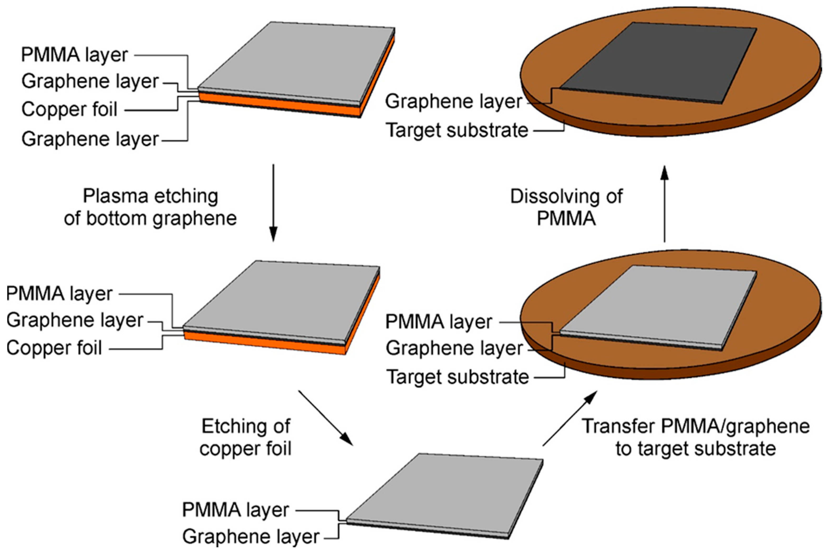
In these experiments, we used commercial graphene samples (Graphenea) synthesized on copper foil using the chemical vapor deposition (CVD) method and covered with a 65 nm layer of poly-methyl methacrylate (PMMA) on one side (see
Figure 1). Graphene was transferred onto silicon 275 μm wafers covered with a layer of Al
2O
3 (96 nm) or TiO
2 (150 nm) using atomic layer deposition (ALD). Additionally, we used a commercially available silicon wafer covered with a 3 μm thick layer of thermally grown SiO
2.
The transfer process started with etching graphene on the side of the copper foil not covered with PMMA using an Oxford Instruments PlasmaLab80 etcher. Then, to dissolve the copper foil and get the graphene ready for transferring, we left the copper with graphene overnight in an iron chloride (FeCl3) solution consisting of 90 g of FeCl3 and 200 mL deionized water. After that, we moved the graphene/PMMA layer to a beaker with deionized water to wash away the remains of the FeCl3 solution. Next, we transferred the graphene to another beaker with new deionized water five times. Then we transferred the graphene with PMMA on the target substrates and let it dry overnight. We next removed the PMMA layer by keeping it in acetone for 30 min and dried the sample under air for 5 min. After that, each sample was washed in isopropanol for 5 min, dried under air, washed in deionized water and dried one more time.
The samples were characterized by measuring their Raman spectra in the 1100 to 3500 cm−1 range by using 514 and 785 nm excitation wavelengths at 25 and 150 mW power, respectively.
As the main characterization technique, we employed transmission spectroscopy. The transmission of the samples in the THz range was studied with a time-domain spectrometer (TDS) (TeTechS, Waterloo, ON, Canada) based on a femtosecond laser with 795 nm in the transmission geometry with an aperture of 3 mm wavelength.
3. Results and Discussions
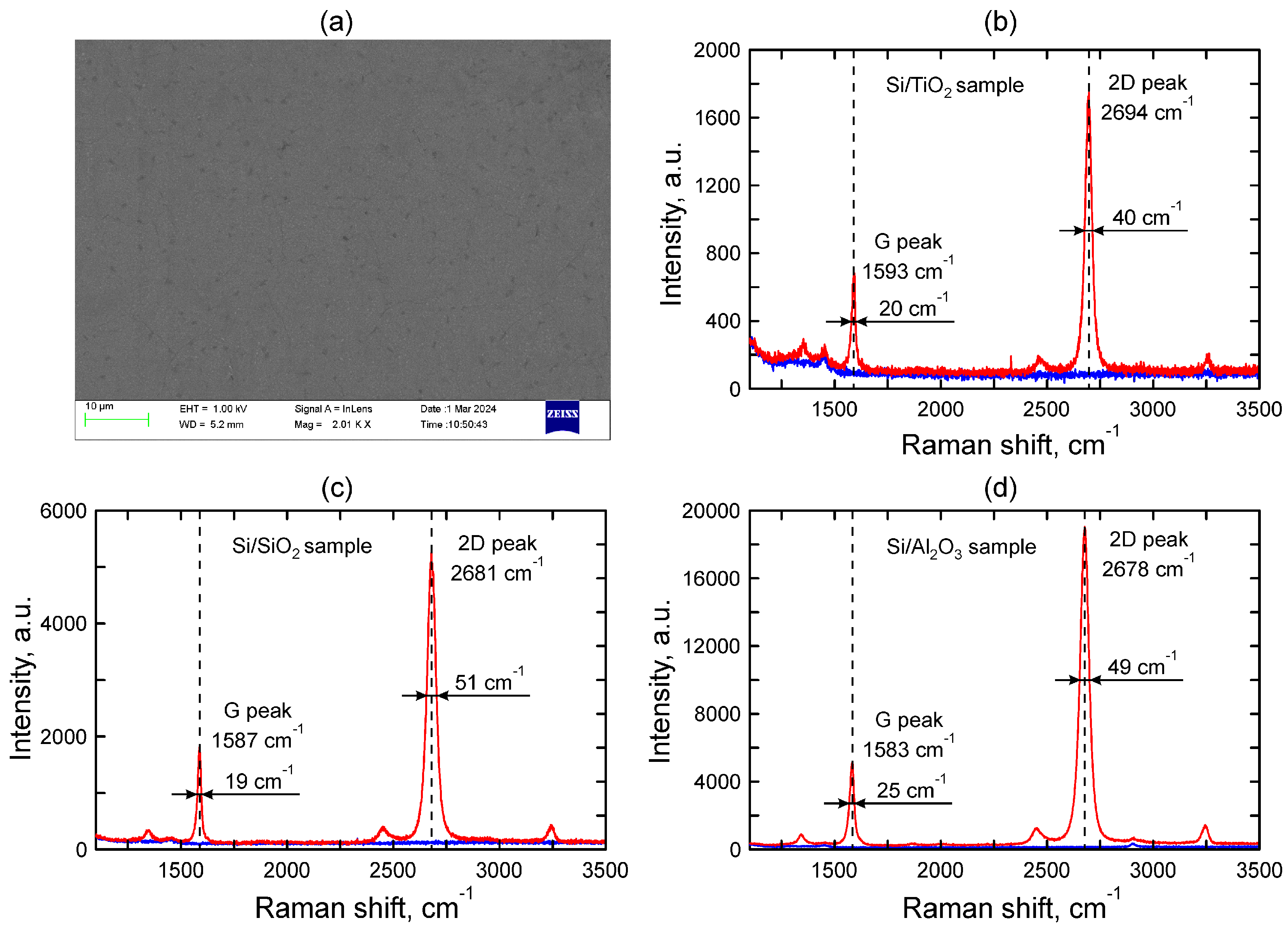
Figure 2a shows the SEM image of the graphene deposited onto a dielectric substrate. The Raman spectra of the TiO
2, SiO
2, and Al
2O
3 substrates (blue curves) with the graphene on them (red curves) are shown in
Figure 2b–d, respectively. One can see that the SEM image is typical for graphene and that the spectra are dominated by D, G and 2D peaks. The D-peak lying around 1360 cm
−1 is low in comparison with both the G and 2D peaks for each sample, which means that the graphene does not have a lot of defects. The intensity
I2D of the 2D peak was more than two times that of the G peak (
IG) for all samples. It is an indication of an unbent monolayer graphene. The exact peaks’ positions and
I2D/
IG ratios are presented in
Table 1.
THz transmission spectroscopy allows one to measure the graphene surface conductivity (inverse of the sheet resistance) non-invasively [
23], avoiding the lithography and metallization process required for the four-probe sheet resistance measurements. This approach was proven to be efficient in previous works. In our work, we used the transfer matrix method [
22] and the Drude model for dynamic dielectric permittivity to analyze the measured spectra. We first fit the measured and simulated spectra for the bare substrate to extract the Drude parameters (DC conductivity and scattering time) of the silicon wafer and then used the same approach for graphene by fitting the corresponding spectra of graphene-coated substrates.
The thickness and refractive index of the silicon wafer were obtained from the time traces measured with the TDS.
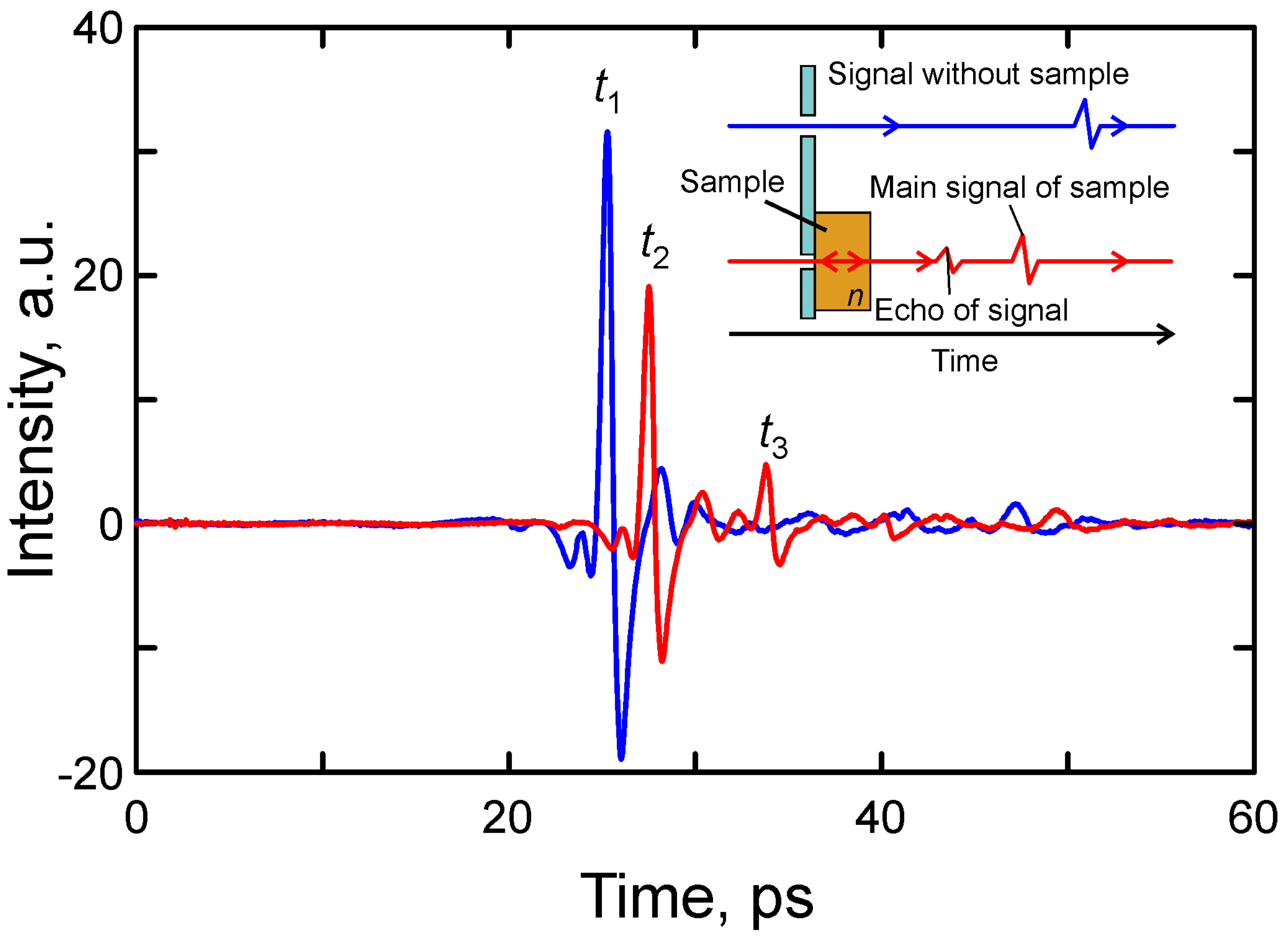
Figure 3 demonstrates typical time traces of the signal recorded in the case of an empty aperture (blue curve) and the case of a Si/TiO
2 substrate. The time trace of the signal in the case of the Si/TiO
2 substrate is delayed relative to the case of the empty aperture and has an additional echo because of reflections inside the substrate (see
Figure 3, inset). Based on these two time traces we can calculate the refractive index
and thickness
of the substrates according to the following equations:
where
is the speed of light in a vacuum and
,
and
are illustrated in
Figure 3. The results for all of the used substrates are summarized in
Table 1. We note that the thicknesses of the silicon wafers we obtained using this method match the results of the direct measurements and the wafer thickness value provided by the producer. The calculated refractive indexes and thickness are presented in
Table 2 along with the thicknesses
dmeas measured with a micrometer and one can see that they approximately match.
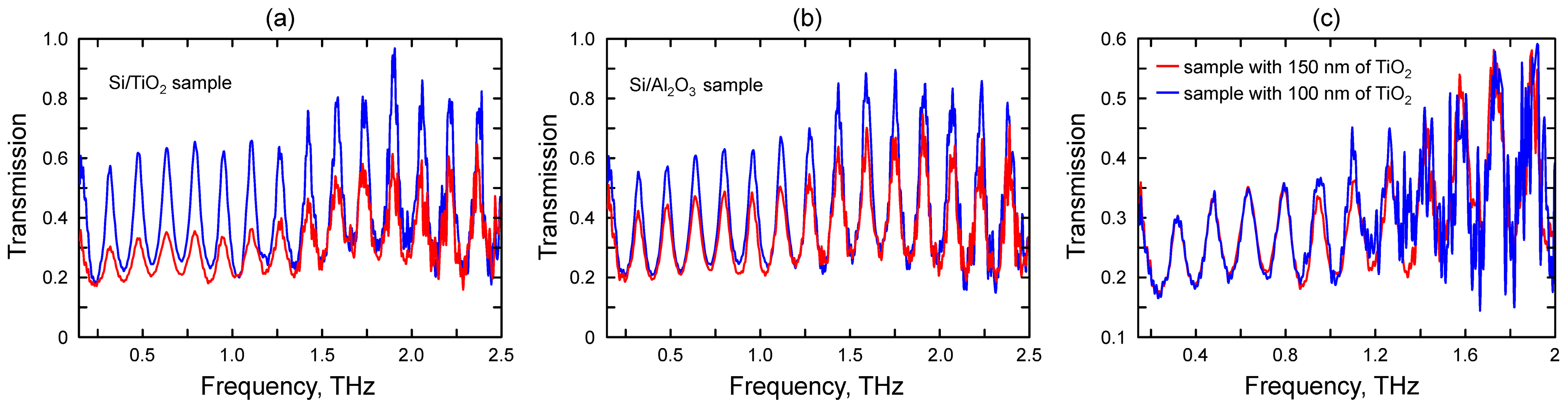
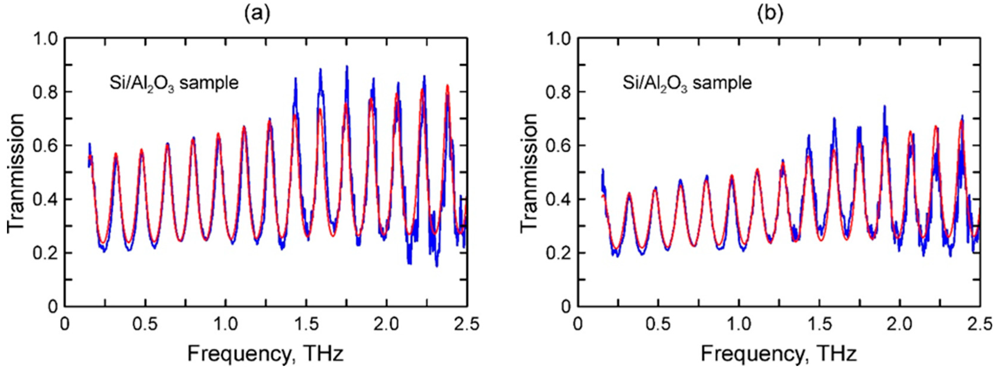
The THz transmission spectra of the substrates covered with graphene and without it are illustrated in
Figure 4a,b. The Fabri–Perot oscillations with a period depending on the substrate’s thickness and refractive index are seen in each graph. We also note that in the case of the bare substrate, transmittance tends to grow with frequency. This already indicates that the Drude scattering time is comparable with the inverse of the characteristic frequency. Transmission of the graphene-coated substrates is lower than that of the bare ones in all frequency ranges due to the intrinsic conductance of the graphene.
Figure 4c shows the THz transmission spectra of the silicon substrates with 150 nm and 100 nm layers of TiO
2. One can see that the spectra match well enough. This illustrates first the overall level of the reproducibility of the results. Secondly, it shows the lack of an effect of the dielectric layer thickness on the THz transmission spectra.
The propagation of the radiation through the sample can be described in terms of the transfer matrix method [
22], which allows us to calculate the transmission, reflection, and absorption through a stack of parallel layers with known dielectric functions
(the magnetic susceptibility is assumed to be the unit). The dielectric function of both the substrate and silicon are described within the Drude model, implying as follows:
where ω is the frequency of the incident THz radiation and σ
0 is the DC conductivity σ(ω = 0). We first fit the transmission of the bare substrates using the silicon DC conductivity and scattering time as fitting parameters. Importantly, the silicon refractive index thickness is defined directly from the time traces. The scattering time turns out to be about 100 fs, consistent with previous studies [
24], while the conductivity ranges from 10 to 30 S/m. Importantly the thickness of the ALD grown dielectric is much smaller that the radiation wavelength, so taking it into account does not affect the results of the simulations. This justifies considering the substrate as a uniform wafer with the thickness and refracted index evaluated based on the time traces. The same applies to the silica-on-silicon substrates. Next, we used the obtained dielectric function of the wafer and fit the transmission spectrum of the graphene-coated substrate to evaluate the sheet resistance
Rsh = 1/σ
s and scattering for the graphene layer. In order to use Equations (3) and (4) for the graphene, we assume that the graphene sheet thickness is
d = 0.35 nm. Still, the obtained value of the graphene sheet resistance does not depend on the graphene sheet thickness
d, which is much smaller than both the wavelength and skin depth.
A comparison of the simulated and measured transmission spectra of the bare substrates is illustrated in
Figure 5a and for the graphene-coated substrates in
Figure 5b. The resulting characteristics of the graphene evaluated based on the transmission spectra are shown in
Table 3.
The results obtained show that the sheet resistance of the graphene significantly depends on the substrate where it is placed. It varies from 350 Ω/sq for graphene on Si/TiO
2 to 900 Ω/sq for graphene on Si/Al
2O
3 with an intermediate value of 550 Ω/sq for graphene on Si/SiO
2. This allows us to suppose that the electronic properties of the substrate affect the Fermi level of the graphene due to the different levels of its doping. The scattering time of graphene derived from the calculated transmission spectra was about 80 ± 10 fs for all samples. Such a value corresponds to a mean free path of about 0.1 μm, which is typical for CVD-grown graphene [
25]. The fact that the mean free path is the same for all graphene samples indicates that the concentration of defects does not depend on the substrate and is related only to the transfer of graphene and the CVD growth process. Correspondently, the difference in sheet resistance is determined mainly by the difference in the charge carriers’ concentration n
s and we may describe its transport properties in terms of the semiclassical Boltzmann transport theory [
26]. Since in our case E
F >> k
BT (degenerate Fermi gas), we may write an equation for the conductivity of 2D materials using the relaxation time calculated as follows:
where
σS = 1/
Rsheet—sheet conductivity. Correspondingly,
where
e = 1.6 × 10
−19—electron charge,
υf = 10
6 m/s—Fermi velocity. We found that
ns = 4.5 × 10
12 cm
−2 for Si/TiO
2, 1.8 × 10
12 cm
−2 for Si/SiO
2 and 0.7 × 10
12 cm
−2 for Si/Al
2O
3.
It is informative to relate the graphene carrier concentration evaluated based on the transmission spectra to the Raman spectra of the corresponding samples. The graphene on the Si/TiO
2 substrate had the highest charge concentration, and at the same time, its G and 2D peaks had the biggest Raman shift. The lowest Raman shifts were registered for graphene on Si/Al
2O
3, and the intermediate parameters belonged to graphene on the Si/SiO
2 substrate; in other words, the greater the charge carrier’s concentration, the greater the Raman shifts of the G and 2D peaks. These results are consistent with the previous studies. According to [
27], the charge concentration of graphene affects its Raman spectra. We used the results of ref [
21] and the position of the G-peak in the measured Raman spectra to estimate the charge carrier concentration; see the last row of
Table 1. The good match between the obtained concentration values provides solid ground for the reliability of our analysis. We note that the use of transmission spectroscopy allows for better accuracy in the evaluation of the carrier concentration, while the Raman data are used in our case for independent verification of these data.
Importantly, our data cannot be used to draw any conclusions on the carrier type. In other words, in no case can we tell whether graphene is p- or n- doped. Further studies will be needed to resolve this issue. Still, the absolute value of the charge carrier concentration is by itself a very important characteristic.


 ,
, 
