Article

Defect Passivation for Highly Efficient and Stable Sn-Pb Perovskite Solar Cells

State Key Laboratory of Dynamic Measurement Technology, North University of China, Taiyuan 030051, China
*
Authors to whom correspondence should be addressed.
Crystals 2024, 14(9), 802; https://doi.org/10.3390/cryst14090802
Submission received: 28 July 2024 / Revised: 3 September 2024 / Accepted: 6 September 2024 / Published: 11 September 2024

Abstract

:
Sn-Pb perovskite solar cells, which have the advantages of low toxicity and a simple preparation process, have witnessed rapid development in recent years, with the power conversion efficiency for single-junction solar cells exceeding 23%. Nevertheless, the problems of poor crystalline quality of Sn-Pb perovskite films arising from rapid crystallization rate and facile oxidation of Sn2+ to Sn4+ have become key issues for the further development of Sn-Pb perovskite solar cells. Herein, we report the incorporation of triazinamide (N-(6-methyl-3-oxo-2,5-dihydro-1,2,4-Triazin-4(3H)-YL) acetamide) as an additive to regulate the crystalline growth of Sn-Pb perovskite films, resulting in films with low trap density and large grain size. The triazinamide additive effectively passivated defects in the perovskite films. As a result, the triazinamide-modified perovskite solar cells achieved a higher efficiency of 15.73%, compared with 13.32% for the control device, significantly improving device performance. Notably, the optimal triazinamide-modified perovskite solar cell maintained 72% of its initial power conversion efficiency after being stored in an air environment for nearly 300 h, while only 18% of the power conversion efficiency of the control perovskite solar cell was retained. This study proposes an effective strategy for fabricating highly efficient and stable Sn-Pb perovskite solar cells.

1. Introduction

Perovskite materials have emerged as promising candidates for solar cells due to their advantages of low exciton binding energy, high light absorption coefficient, long carrier diffusion distance and high defect tolerance [1,2,3]. Among them, organic–inorganic hybrid perovskites have received considerable attention in the field of solar cells. Currently, the power conversion efficiency (PCE) of Pb-based single-junction perovskite solar cells (PSCs) can exceed 26% [4,5,6]. However, Pb-based perovskites cause Pb leakage, which is toxic to the environment and organisms and hinders their widespread application. Sn-based perovskites have less impact on the environment, as Sn is oxidized to SnO2 when it comes into contact with air, which is ecologically friendly. Compared with Pb, Sn has a similar ionic radius and electronic properties [7,8], but Sn2+ in pure Sn-based perovskite is easily oxidized to Sn4+, which seriously affects the stability of perovskite films. On the basis of Pb-based perovskites, the oxidation of Sn2+ can be inhibited to some extent by replacing Pb with a certain amount of Sn. Moreover, the bandgap of Sn-Pb perovskites can be regulated by changing the ratio of Sn and Pb, which helps to break through the detailed balance limit of single-junction solar cells [9,10,11,12] to further develop tandem solar cells. Therefore, Sn-Pb PSCs are an important research direction for reducing toxicity and fabricating highly efficient and stable devices.
At present, researchers generally use chemical methods to improve the performance of perovskite solar cells, which pose a certain hidden danger to the environment, and researchers have also tried to improve the performance of devices by physical methods. The plasma effect is an effective method to improve the light absorption capacity of perovskite thin films [13]. For example, Wu et al. inserted Au@SiO2 nanorods between a PEDOT:PSS layer and a CH3NH3PbI3 layer; Au@SiO2 nanorods were able to stimulate local surface plasmonic resonance, improve incident light capture, and improve carrier transport and collection in the device. The average efficiency of the device was increased by more than 40% [14]. In Sn-Pb PSCs, this method is also worth exploring, but at present, the problem of the poor quality of perovskite films is more prominent.
Although Sn-Pb PSCs have developed rapidly in recent years, the oxidation of Sn2+ introduces numerous Sn2+ vacancies in the perovskite lattice, leading to a large number of defects and resulting in poor device stability. Additionally, the rapid reaction between SnI2 and organic iodide complicates the control of films’ crystallization, making it difficult to achieve high-quality perovskite films and PSCs [11]. This is the main obstacle to the development of Sn-Pb PSCs, and the quality of perovskite films urgently needs to be improved.
Additive engineering and post-treatment methods are used to reduce defects, improve the quality of perovskite films, and facilitate carrier transport [15,16,17,18,19,20,21]. For example, Lin et al. proved that metal Sn as a reducing agent can reduce the concentration of Sn4+ in the precursor solution, thereby reducing the defect density of perovskite and improving the quality of perovskite films [22]. Liu et al. demonstrated that caffeic acid (CA) can retard the oxidation of Sn2+ and improve the quality of perovskite films [23]. For interface engineering, Hayase et al. introduced ethylenediamine (EDA) molecules to passivate Sn-Pb perovskite surface defects, transforming the perovskite surface’s P-type semiconductor properties to N-type, forming a gradient band structure to promote interfacial charge transport [24]. In addition, phenylethylammonium (PEA) cation can react with perovskite to form a 2D surface layer, passivating the surface of Sn-Pb perovskite film, thereby improving the stability of the film [25]. Zhang et al. introduced an ionic salt layer of iso-pentylammonium tetrafluoroborate ([PNA]BF4) as an anchoring agent, balancing the crystallization rate of Sn-Pb perovskites [26]. Luo et al. doped cysteine hydrochloride (CysHCl) into a Sn-Pb perovskite precursor and used it for post-treatment of the Sn-Pb perovskite surface, which effectively inhibited Sn2+ oxidation, improved perovskite crystal quality, reduced trap density, and promoted the rapid transfer of charge carriers [27]. Lv et al. used MAAc to improve the antioxidant capacity of the precursor solution through the coordination of abundant hydrogen bonds with the Sn-Pb precursor solution and successfully prepared Sn-Pb perovskite films in air [28]. Recently, the PCE of Sn-Pb PSCs prepared via the one-step method has continuously improved, finally reaching 23.7% [29,30,31]. In contrast, the PCE of Sn-Pb PSCs prepared using the two-step method has develop slowly [32,33]. It is well known that the one-step deposition method needs to use a lot of antisolvent, which makes the fabrication process more demanding and less reproducible. In contrast, the more controllable and environmentally friendly two-step method is expected to produce PSCs on a large scale. In the two-step method, the quality and stability of perovskite films are worse, and there are fewer additives that can simultaneously inhibit the oxidation of Sn2+ and regulate the crystallization of the films. Therefore, it is very important to develop effective additives to achieve simultaneous improvement of device efficiency and stability.
The O atom of carbonyl (C=O) has a lone pair of electrons and strong electron donor ability, making it able to form coordination bonds with metal elements and effectively passivate defects [34]. The interaction between C=O and Sn atoms can inhibit the oxidation of Sn2+ and reduce the generation of defect states [34]. Amino groups can also regulate the growth process of perovskite crystals through hydrogen bond interactions (N-H···I) [15]; however, the synergistic passivation of multiple carbonyl and amino groups in two-step tin–lead hybrid perovskite solar cells has not been well explored.
In this work, we report a defect regulation strategy for Sn-Pb PSCs incorporating NAT into a PbI2/SnI2 precursor solution. The triazinamide (N-(6-methyl-3-oxo-2,5-dihydro-1,2,4-Triazin-4(3H)-YL) acetamide (NAT)) molecule contains two carbonyl groups and amino groups, which can interact with metal elements and organic cations at the same time, slowing down the reaction rate between metal elements and organic cations in order to better adjust the growth of perovskite crystals. The NAT modification strategy reduced the defects of Sn-Pb perovskite films and improved the performance of Sn-Pb PSCs. NAT was effectively able to coordinate with Sn2+, preventing its oxidation to Sn4+ and significantly reducing the formation of defects within the perovskite films. Benefiting from these reduced defects, the PCE of the PSC increased from 13.32% to 15.73%, and the PSC also shows enhanced environmental stability, maintaining 72% of the initial efficiency after nearly 300 h of testing.

2. Experiment

2.1. Materials

ITO conductive glass was purchased from Suzhou Shangyang Solar Energy Technology Co., Ltd. (Suzhou, China); dimethylformamide (DMF, with purity 99.90%), Dimethyl sulfoxide (DMSO, 99.80%), anhydrous ethanol (C2H5O, 99.70%), isopropyl alcohol (C3H8O, 99.00%), and chlorobenzene (C6H5Cl, 99.80%) were all purchased from Aladdin; lead iodide (PbI2, 99.99%), phenyl-C61-methyl butyrate (PC61BM, 99.50%), formamidine iodide (FAI, 99.50%), methylamine chloride (MACl, 99.50%), Bphen (BCP, 99.00%), and poly(3,4-ethylenedioxyethiophene)-poly(styrene sulfonic acid) (PEDOT:PSS) aqueous solution (Al 4083) were purchased from Xi’an Yuri Soler Co., Ltd. (Xi’an, China); stannous iodide (SnI2, >97.00%) and triazinamide (N-(6-methyl-3-oxo-2,5-dihydro-1,2,4-Triazin-4(3H)-yl)acetamide) (C6H10N4O2, 99%, abbreviated as NAT) were purchased from TCI.

2.2. Device Fabrication

2.2.1. ITO Conductive Glass Treatment

ITO conductive glass was ultrasonicated three times in anhydrous ethanol for 10 min each time, and then dried in an oven at 60 °C. Before use, the cleaned ITO conductive glass was treated with UV ozone (UVO) for 20 min to effectively remove surface organic matter.

2.2.2. Hole Transport Layer (ETL) Fabrication

To enable fabrication of the hole transport layer, 150 μL of PEDOT:PSS solution was spin coated on top of the ITO conductive glass at 5000 r/min for 30 s and annealed at 150 °C for 20 min for future use.

2.2.3. Precursors Preparation and Perovskite Film Fabrication

The precursor solution of PbI2/SnI2 was obtained by dissolving PbI2 (419.5 mg) and SnI2 (145.3 mg) in mixed solvent [DMF (800 μL)/DMSO (200 μL)]. This was stirred at room temperature for 12 h and fully filtered to obtain a light yellow solution. Different amounts of NAT were added to obtain PbI2/SnI2 solutions with NAT concentrations of 1 mg/mL, 2 mg/mL, and 4 mg/mL, respectively. The FAI solution was obtained by dissolving FAI (60 mg) and MACl (14 mg) into 1 mL isopropyl alcohol and was fully dissolved before use. The perovskite precursor solution of PbI2/SnI2 with or without NAT additive was deposited onto the PEDOT:PSS according to a program at 1500 r/min for 30 s. Then, the film was quickly transferred onto a hotplate and annealed at 70 °C for 2 min, after which the PbI2/SnI2 film was cooled down for 30 min. The FAI solution was spin coated onto the PbI2/SnI2 film at 4000 r/min for 30 s, then annealed on a hotplate at 50 °C for 2 min, then subsequently annealed at 120 °C for 10 min, achieving FAnMA1-nPb0.7Sn0.3IxCl3−x film.

2.2.4. Electron Transport Layer Fabrication

The PC61BM solution was obtained by dissolving PC61BM (20 mg) into 1 mL chlorobenzene, filtered, and set aside for use. Then, 50 µL solution was spin coated on top of the perovskite film at 3000 r/min for 30 s.

2.2.5. BCP Layer Fabrication

The BCP solution was obtained by dissolving BCP (0.5 mg) into 1 mL isopropyl alcohol, filtered, and set aside for use. Then, 50 µL solution was spin-coated on top of the perovskite film at 5000 r/min for 30 s.

2.2.6. Metal Electrode Fabrication

The vacuum evaporation coater (vacuum < 1 × 10⁻⁵ Pa) was used for the physical vapor deposition of silver electrode with a thickness of about 80 nm.

2.3. Characterizations

X-ray diffraction (XRD) tests were carried out using a Bruker D8 Discover XRD diffractometer (Bruker Corporation, Karlsruhe, Germany) with Cu-Kα (λ = 0.15406 nm) as the target material. The ultraviolet–visible absorption spectrum (UV-Vis) of the samples was measured using a Shimadzu 3600 UV–visible–NIR spectrophotometer (Shimadzu Corporation, Kyoto, Japan). The solar cell efficiency was measured using an XES 40S1 SAN-EI solar simulator (SAN-EI Electric Co., Ltd, Osaka, Japan) with a Keithley 2400 source meter (Keithley Instruments, Berea, KY, USA). The light intensity of the solar simulator was 100 mW/cm2, measured by photometer (International Light, IL1400) and corrected with standard silicon solar cells. The external quantum efficiency (EQE) of the samples was measured using a quantum efficiency measuring instrument (QE-R, Guangyan Technology Co., Ltd., Hangzhou, China). The morphology of the perovskite films was characterized by FEI Nova_Nano SEM 430 (Thermo Fisher Scientific, Malborne, FL, USA). The Keithley 2400 source meter was used to measure the current and voltage of the hole-only devices. transient photovoltage (TPV) decay tests, transient photocurrent (TPC) decay tests, and electrochemical impedance spectroscopy were measured with a German Zahner electrochemical workstation (Zahner-Geräte GmbH, Dresden, Germany). The capacitance–voltage characteristics of the devices was measured with a Keysight E4990A impedance analyzer (Keysight Technologies, Santa Rosa, CA, USA).

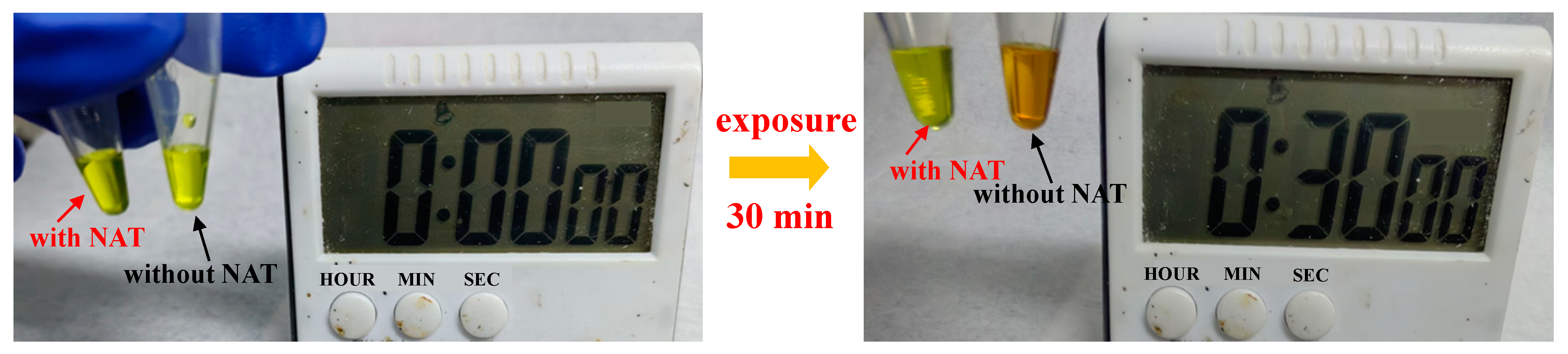
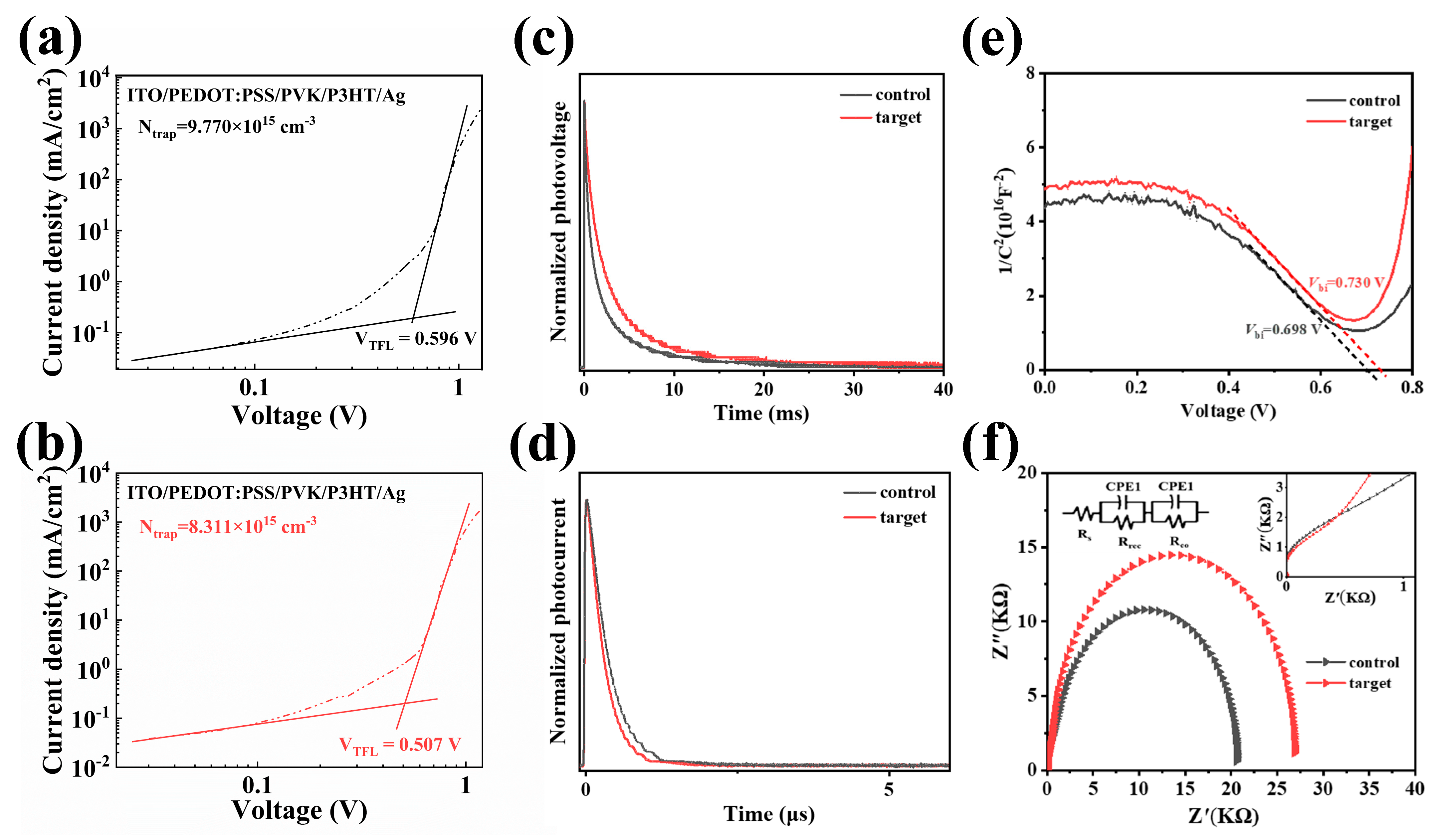
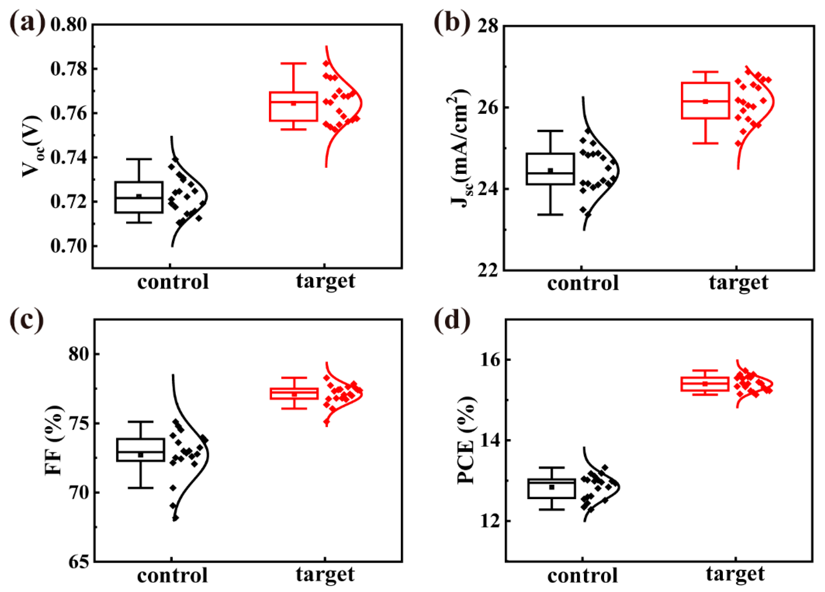
3. Results and Discussion

In this work, the SEM characterization of the perovskite films was firstly carried out, and the results are shown in Figure 1. According to the top-view SEM images of the perovskite films, the surface of the control perovskite film had a small and uneven grain size, with more obvious grain boundaries and holes; the average grain size was 423.8 nm, which was attributed to the rapid reaction between SnI2 and FAI forming a perovskite film with a poorer crystalline quality [32]. The quality of the NAT-modified perovskite films was significantly improved, with a larger grain size and denser and more uniform surfaces; the average grain sizes of the NAT-modified films with different concentrations of NAT (Figure 2) were 437.1 nm (1 mg/mL), 865.7 nm (2 mg/mL), 713.9 nm (4 mg/mL), respectively. When the concentration of NAT was 2 mg/mL, the crystal quality of the perovskite film was at its best. This indicates that the appropriate concentration of NAT can promote the growth of perovskite crystals and increase the grain size of perovskite films, which could reduce defect density in the films, promote charge extraction, and improve the performance of devices [35]. For comparison, the PSC and perovskite film without NAT was termed the control, and the optimal concentration NAT-modified film and device were designated as the target.
Furthermore, as can be seen from the cross-sectional SEM images in Figure 3, the thickness of the control perovskite film was 451 nm, and the target perovskite was 473 nm. The control perovskite film was composed of some small grains and the grain boundaries were obvious, which would hinder carrier transport and cause carrier recombination. In contrast, the cross-sectional quality of the target perovskite film was higher, the grain size was large, the grain boundaries less obvious, and the grain distribution uniform and orderly. The perovskites grew along the vertical direction of the substrate, and the carrier transport did not encounter the grain boundary, which was conducive to reducing the non-radiative recombination of carriers, thus improving the performance of the film and the device.
To investigate the changes in the crystalline quality of the perovskite films, UV–Vis absorption spectroscopy was performed. As shown in Figure 4a, compared with the control film, the absorption capacity of the target film was significantly enhanced in the range of 400 nm to 550 nm, indicating reduced defects in perovskite film and improved crystal quality. Moreover, the absorption range and absorption band edge of the target film remained similar to the control film, indicating that the introduction of NAT did not alter the bandgap of the perovskite. The Tauc plot was used to estimate the bandgap of perovskite. As shown in Figure 5, the bandgaps of the control (Figure 5a) and NAT-modified (Figure 5b) perovskite films were 1.348 eV and 1.346 eV, respectively.
The crystalline quality of perovskite has a great influence on the film quality. To gain further insights into the impact of NAT on the crystalline growth of perovskite, X-ray diffraction (XRD) measurements were conducted. As depicted in Figure 4b, the XRD patterns revealed prominent diffraction peaks centered around 14°, 24°, and 28°, corresponding to the (110), (202), and (220) crystal planes of perovskites, respectively [36,37]. Compared with the control film, the target film showed higher intensity at the (202) peak, signifying higher crystallinity of the perovskite. Conversely, the diffraction peak intensities of the (110) and (220) crystal planes were low, suggesting that perovskite crystals had a preferential growth orientation along the (202) crystal plane, advantageous for expanding the grain size of the perovskite and promoting the improvement of film quality. The peak intensity ratios of (202)/(110) and (202)/(220) increased respectively from 2.7 and 2.6 for the control perovskite film to 9.6 and 8.6 for the NAT-modified perovskite film, indicating that the interaction between NAT and the perovskite precursor slowed down the crystallization rate of the perovskite and made the crystallinity of the perovskite higher. This result was basically consistent with the SEM characterization results.
To study the potential of NAT in slowing down the oxidation process of Sn2+, we formulated PbI2/SnI2 solution with and without NAT and exposed them to air. As shown in Figure 6, after 30 min of exposure to the air, the PbI2/SnI2 solution without NAT underwent a discernible color change from light yellow to brown, while the PbI2/SnI2 solution with NAT remained light yellow. This phenomenon can be attributed to the presence of two C=O bonds in the NAT molecule, wherein the oxygen atoms possess lone pairs of electrons capable of coordinating with Sn2+, thus inhibiting the production of Sn4+. Moreover, in perovskite films, the C=O bonds can passivate uncoordinated Sn2+, Pb2+, and iodine vacancies, ultimately reducing the defect state densities of the perovskite films [34].
To further quantitatively characterize the effect of NAT on the defect density of perovskite films, a space-charge-limited current (SCLC) test was performed with a hole-only device [38]. The trap filling limit voltages (VTFL) for control and target hole-only devices were determined to be 0.596 V and 0.507 V, respectively (Figure 7a,b). The density of defect states can be calculated by Formula (1):
Ntrap = (2VTFLεε0)/(eL2)
where Ntrap is the trap state density of the device, e is the elementary charge, ε0 is the vacuum dielectric constant, ε is the relative dielectric constant, and L is the film thickness. The calculated hole-defect density of the target device was 8.311 × 10¹⁵/cm3, lower than that of control device (9.770 × 10¹⁵/cm3). The decrease in defect density in the target device indicated that the introduction of NAT was better able to inhibit Sn2+ oxidation and reduce the generation of defects in the Sn-Pb perovskite film.
Furthermore, to verify the charge transport and recombination dynamics in PSCs, transient photocurrent (TPC) decay testing and transient photovoltage (TPV) decay testing were carried out. The results are shown in Figure 6. In the TPV test (Figure 7c), the transient photovoltage decay time of the control device was 2.077 ms, while that of the target device was 2.981 ms. The prolonged transient photovoltage decay time signified the suppressed carrier recombination in the target device. The TPC test (Figure 7d) showed that the transient photocurrent decay time of the control device was 0.369 μs, while that of the target device was only 0.299 μs, indicating that the carrier extraction efficiency of the PSC was higher after NAT modification. The faster carrier transport and the reduction in carrier recombination underscore the capability of NAT to enhance device performance.
Next, Mott–Schottky measurements were performed to delve deeper into the effect of NAT on the device’s built-in electric field (Vbi). As indicated in Figure 7e, the control device had a Vbi of 0.698 V, while the target device showed an increase in Vbi to 0.730 V. The increase in Vbi signifies an improved driving force for charge separation and transport within the device. Then, the carrier transport behavior was analyzed by electrochemical impedance spectroscopy (EIS). As illustrated in Figure 7f, the target device exhibited a series resistance (Rs) of 1.63 Ω and a recombination resistance (Rrec) of 26.10 KΩ, while the control device had an Rs of 9.78 Ω and an Rrec of 19.35 KΩ. The lower Rs and higher Rrec for the target device confirm the enhancement of charge transport efficiency and suppression of carrier recombination.
The reduction in defects in perovskite films coupled with the improved carrier transport characteristics contributed significantly to the overall performance enhancement of the PSCs. To quantify the effect of NAT additive on the photoelectric performance of Sn-Pb PSCs, a series of characterizations of PSCs was conducted on devices with a structure of ITO/PEDOT:PSS/PVK/PC61BM/BCP/Ag. Firstly, the doping concentration of NAT in the PbI2/SnI2 solution was optimized, and the corresponding photoelectric performance parameters are shown in Table 1. Notably, the PCE of all NAT-modified devices exceeded that of the control devices, with improvements observed in open-circuit voltage (VOC), short-circuit current density (JSC), and fill factor (FF). Specifically, at an optimal NAT concentration of 2.0 mg/mL, the PCE was 15.73%, significantly outperforming the control PSC with a PCE of 13.32%. This improvement was accompanied by enhancements in JSC, VOC, and FF, which increased from 24.67 mA/cm2 to 26.80 mA/cm2, 0.72 V to 0.76 V, and 0.75 to 0.78, respectively. The corresponding statistical photovoltaic performance parameters (Figure 8) illustrate the strong reproducibility of the target devices. Figure 9a more clearly illustrates the positive impact of NAT doping on the photovoltaic performance of Sn-Pb PSCs. The forward and reverse scan curves and device parameters of the optimal NAT-modified and control PSC are shown in Table 2. It was observed that due to defect passivation, the hysteresis index (HI) of the optimal NAT-modified device was only 1.01%, which was smaller than that of the control device with HI = 4.43%. These improvements can be attributed primarily to the reduction in defects in the perovskite films and the suppression of non-radiative carrier recombination, leading to reduced losses in the charge transfer process.
Figure 9b presents the EQE and integrated current density curves of the control and target PSCs. It can be seen from the EQE spectra that the target PSC had a higher EQE value, where EQE is the ratio of the number of photons incident on the device to the number of charges collected by the electrode and is related to the quality of perovskite film and the charge transport ability of the device. The high EQE value indicates that the target perovskite film had higher crystal quality, better light absorption, and faster carrier transport. The integrated current density value of 23.62 mA/cm2 for the control PSC and 25.82 mA/cm2 for the target PSC were in good agreement with the JSC value obtained from the J-V curves, indicating the reliability and accuracy of the experimental measurement. However, the device performance deteriorated when the concentration of NAT increased to 4 mg/mL, with the PCE dropping to 15.18%. The main reason was that the excessive amount of NAT inhibited the crystallization and growth of the perovskite film, resulting in poor crystalline quality and ultimately lowering the PCE. Figure 9c shows the steady-state output PCE of the PSCs at the maximum power point (MPP) over 300 s. The target PSC exhibited a stable PCE of 15.13%, significantly higher than the 12.89% of the control PSC. This result underscores the improved stability and PCE of the NAT-modified PSCs, further emphasizing the importance of the NAT doping strategy in enhancing the performance of Sn-Pb PSCs.
Finally, the moisture stability of unencapsulated control and target PSCs was tested under ambient conditions (relative humidity of 20–30% at 25 °C in air). From the normalized PCE variation curves (Figure 9d), it was confirmed the stability of target PSC was superior to that of control PSC. After storing for over 300 h, the target PSC was able to maintain 72% of its initial PCE, while the control PSC could maintain only 18% of its initial PCE after the same aging time. This result highlights the significant improvement in moisture stability achieved through the introduction of NAT.

4. Conclusions

In conclusion, this study has successfully demonstrated a very effective strategy of introducing NAT as an additive into PbI2/SnI2 precursor solution for preparing high-quality perovskite films and devices. The NAT additive played an important role in regulating the growth of perovskite crystals during the two-step deposition process, inhibiting the oxidation of Sn2+, and passivating defects within the perovskite films. As a result, high-quality perovskite films with larger perovskite grain size and fewer defects were obtained. The target PSC achieved a PCE exceeding 15%, accompanied by superior environmental stability. This study provides an effective method for fabricating high-quality Sn-Pb perovskite films and highly efficient and stable PSCs.

Author Contributions

Conceptualization, T.L. (Tengteng Li), M.L. and C.L.; methodology, T.L. (Tengteng Li), M.L. and C.L.; software, T.L. (Tengteng Li), F.M. and Y.H.; validation, T.L. (Tengteng Li), F.M., Y.H., H.W., P.Z. and Z.L.; formal analysis, T.L. (Tengteng Li), F.M., Y.H., H.W., P.Z. and Z.L.; investigation, F.M., Y.H., H.W., P.Z. and Z.L.; resources, T.L. (Tengteng Li); data curation, T.L. (Tengteng Li); writing—original draft preparation, T.L. (Tengteng Li); writing—review and editing, T.L. (Tengteng Li) and F.M.; visualization, T.L. (Tengteng Li), F.M., Y.H., H.W., P.Z. and Z.L.; supervision, T.L. (Ting Liang), M.L., J.Y. and C.L.; project administration, T.L. (Tengteng Li), M.L. and C.L.; funding acquisition, T.L. (Tengteng Li), F.L. and T.L. (Ting Liang). All authors have read and agreed to the published version of the manuscript.

Funding

This work was supported by the National Natural Science Foundation of China (Nos. 62301509 and 62304209) and Basic Research Program of Shanxi Province (Nos. 202203021222079 and 20210302123203).

Data Availability Statement

Data are contained within the article.

Conflicts of Interest

The authors declare no conflicts of interest.

References

  1. Dong, Q.; Fang, Y.; Shao, Y.; Mulligan, P.; Qiu, J.; Cao, L.; Huang, J. Electron-Hole Diffusion Lengths > 175 μm in Solution-Grown CH3NH3PbI3 Single Crystals. Science 2015, 347, 967–970. [Google Scholar] [CrossRef] [PubMed]
  2. Tan, H.; Jain, A.; Voznxy, O.; Lan, X.; De, A.F.; Fan, J.Z.; Quintero-Bermudez, R.; Yuan, M.; Zhang, B.; Zhao, Y.; et al. Efficient and Stable Solution-Processed Planar Perovskite Solar Cells via Contact Passivation. Science 2017, 355, 722–726. [Google Scholar] [CrossRef]
  3. Zhao, D.; Wang, B.; Song, Z.; Yu, Y.; Chen, C.; Zhao, X.; Zhu, K.; Yan, Y. Four-Terminal All-Perovskite Tandem Solar Cells Achieving Power Conversion Efficiencies Exceeding 23%. ACS Energy Lett. 2018, 3, 305–306. [Google Scholar] [CrossRef]
  4. Kojima, A.; Teshima, K.; Shirai, Y.; Miyasaka, T. Organometal Halide Perovskites as Visible-Light Sensitizers for Photovoltaic Cells. J. Am. Chem. Soc. 2009, 131, 6050–6051. [Google Scholar] [CrossRef]
  5. Kim, M.; Jeong, J.; Lu, H.; Lee, T.K.; Eickemeyer, F.T.; Liu, Y.; Choi, I.W.; Choi, S.J.; Jo, Y.; Kim, H.B.; et al. Conformal Quantum Dot-SnO2 Layers as Electron Transporters for Efficient Perovskite Solar Cells. Science 2022, 375, 302–306. [Google Scholar] [CrossRef]
  6. Zhou, J.; Tan, L.; Liu, Y.; Li, H.; Liu, X.; Li, M.; Wang, S.; Zhang, Y.; Jiang, C.; Hua, R.; et al. Highly Efficient and Stable Perovskite Solar Cells via A Multifunctional Hole Transporting Material. Joule 2024, 8, 1691–1706. [Google Scholar] [CrossRef]
  7. Yang, S.; Fu, W.; Zhang, Z.; Chen, H.; Li, C. Recent Advances in Perovskite Solar Cells: Efficiency, Stability and Lead-Free Perovskite. J. Mater. Chem. A 2017, 5, 11462–11482. [Google Scholar] [CrossRef]
  8. Shi, Z.; Guo, J.; Chen, Y.; Li, Q.; Pan, Y.; Zhang, H.; Xia, Y.; Huang, W. Lead-Free Organic-Inorganic Hybrid Perovskites for Photovoltaic Applications: Recent Advances and Perspectives. Adv. Mater. 2017, 29, 1605005. [Google Scholar] [CrossRef]
  9. Umari, P.; Mosconi, E.; De Angelis, F. Relativistic GW Calculations on CH3NH3PbI3 and CH3NH3SnI3 Perovskites for Solar Cell Applications. Sci. Rep. 2014, 4, 4467. [Google Scholar] [CrossRef]
  10. Rajagopal, A.; Stoddard, R.J.; Hillhouse, H.W.; Jen, A.K. On Understanding Bandgap Bowing and Optoelectronic Quality in Pb-Sn Alloy Hybrid Perovskites. J. Mater. Chem. A 2019, 7, 16285–16293. [Google Scholar] [CrossRef]
  11. Prasanna, R.; Gold-Parker, A.; Leijtens, T.; Conings, B.; Babayigit, A.; Boyen, H.G.; Toney, M.F.; McGehee, M.D. Band Gap Tuning via Lattice Contraction and Octahedral Tilting in Perovskite Materials for Photovoltaics. J. Am. Chem. Soc. 2017, 139, 11117–11124. [Google Scholar] [CrossRef] [PubMed]
  12. Zhao, B.; Abdi-Jalebi, M.; Tabachnyk, M.; Glass, H.; Kamboj, V.S.; Nie, W.; Pearson, A.J.; Puttisong, Y.; Gödel, K.C.; Beere, H.E.; et al. High Open-Circuit Voltages in Tin-Rich Low-Bandgap Perovskite-Based Planar Heterojunction Photovoltaics. Adv. Mater. 2017, 29, 1604744. [Google Scholar] [CrossRef] [PubMed]
  13. Wu, R.; Yang, B.; Zhang, C.; Huang, Y.; Cui, Y.; Liu, P.; Zhou, C.; Hao, Y.; Gao, Y.; Yang, J. Prominent Efficiency Enhancement in Perovskite Solar Cells Employing Silica-Coated Gold Nanorods. J. Phys. Chem. C 2016, 120, 6996–7004. [Google Scholar] [CrossRef]
  14. Jang, Y.H.; Jang, Y.; Kim, S.; Quan, L.; Chung, K.; Kim, D.H. Plasmonic Solar Cells: From Rational Design to Mechanism Overview. Chem. Rev. 2016, 116, 14982–15034. [Google Scholar] [CrossRef]
  15. Mahapatra, A.; Prochowicz, D.; Tavakoli, M.M.; Trivedi, S.; Kumar, P.; Yadav, P. A review of aspects of additive engineering in perovskite solar cells. J. Mater. Chem. A 2020, 8, 27–54. [Google Scholar] [CrossRef]
  16. Yeom, K.W.; Lee, D.K.; Park, N.G. Hard and Soft Acid and Base (HSAB) Engineering for Efficient and Stable Sn-Pb Perovskite Solar Cells. Adv. Energy Mater. 2022, 12, 2202496. [Google Scholar] [CrossRef]
  17. Lin, R.; Xu, J.; Wei, M.; Wang, Y.; Qin, Z.; Liu, Z.; Wu, J.; Xiao, K.; Chen, B.; Park, S.M.; et al. All-perovskite tandem solar cells with improved grain surface passivation. Nature 2022, 603, 73–78. [Google Scholar] [CrossRef] [PubMed]
  18. Wang, G.; Wang, C.; MacKenzie, R.C.I.; Zhu, Z.; Chen, Y.; Ruan, S.; Wen, S. Using Ligand Engineering to Produce Efficient and Stable Pb-Sn Perovskite Solar Cells with Antioxidative 2D Capping Layers. ACS Appl. Mater. Interfaces 2022, 14, 14729–14738. [Google Scholar] [CrossRef] [PubMed]
  19. Yu, D.; Wei, Q.; Li, H.; Xie, J.; Jiang, X.; Pan, T.; Wang, H.; Pan, M.; Zhou, W.; Liu, W.; et al. Quasi-2D Bilayer Surface Passivation for High Efficiency Narrow Bandgap Perovskite Solar Cells. Angew. Chem. Int. Ed. 2022, 61, e202202346. [Google Scholar] [CrossRef]
  20. Sahamir, S.R.; Kamarudin, M.A.; Ripolles, T.S.; Baranwal, A.K.; Kapil, G.; Shen, Q.; Segawa, H.; Bisquert, J.; Hayase, S. Enhancing the Electronic Properties and Stability of High-Efficiency Tin–Lead Mixed Halide Perovskite Solar Cells via Doping Engineering. J. Phys. Chem. Lett. 2022, 13, 3130–3137. [Google Scholar] [CrossRef]
  21. Yuce, H.; Perini, C.A.R.; Hidalgo, J.; Castro-Ménde, Z.A.F.; Evans, C.; Betancur, P.F.; Vagott, J.N.; An, Y.; Bairley, K.; Demir, M.M.; et al. Understanding the impact of SrI2 additive on the properties of Sn-based halide perovskites. Opt. Mater. 2022, 123, 111806. [Google Scholar] [CrossRef]
  22. Lin, R.; Xiao, K.; Qin, Z.; Han, Q.; Zhang, C.; Wei, M.; Saidaminov, M.I.; Gao, Y.; Xu, J.; Xiao, M.; et al. Monolithic all-perovskite tandem solar cells with 24.8% efficiency exploiting comproportionation to suppress Sn(ii) oxidation in precursor ink. Nat. Energy 2019, 4, 864–873. [Google Scholar] [CrossRef]
  23. Liu, H.; Wang, L.; Li, R.; Shi, B.; Wang, P.; Zhao, Y.; Zhang, X. Modulated Crystallization and Reduced VOC Deficit of Mixed Lead-Tin Perovskite Solar Cells with Antioxidant Caffeic Acid. ACS Energy Lett. 2021, 6, 2907–2916. [Google Scholar] [CrossRef]
  24. Kapil, G.; Bessho, T.; Maekawa, T.; Baranwal, A.K.; Zhang, Y.; Kamarudin, M.A.; Hirotani, D.; Shen, Q.; Segawa, H.; Hayase, S. Tin-Lead Perovskite Fabricated via Ethylenediamine Interlayer Guides to the Solar Cell Efficiency of 21.74%. Adv. Energy Mater. 2021, 11, 2101069. [Google Scholar] [CrossRef]
  25. Wei, M.; Xiao, K.; Walters, G.; Lin, R.; Zhao, Y.; Saidaminov, M.I.; Todorovic, P.; Johnston, A.; Huang, Z.; Chen, H.; et al. Combining Efficiency and Stability in Mixed Tin-Lead Perovskite Solar Cells by Capping Grains with an Ultrathin 2D Layer. Adv. Mater. 2020, 32, 1907058. [Google Scholar] [CrossRef]
  26. Zhang, Z.; Liang, J.; Zheng, Y.; Wu, X.; Wang, J.; Huang, Y.; Yang, Y.; Zhou, Z.; Wang, L.; Kong, L.; et al. Balancing Crystallization Rate in A Mixed Sn-Pb Perovskite Film for Efficient and Stable Perovskite Solar Cells of more than 20% Efficiency. J. Mater. Chem. A 2021, 9, 17830–17840. [Google Scholar] [CrossRef]
  27. Luo, J.; He, R.; Lai, H.; Chen, C.; Zhu, J.; Xu, Y.; Yao, F.; Ma, T.; Luo, Y.; Yi, Z.; et al. Improved Carrier Management via a Multifunctional Modifier for High-Quality Low-Bandgap Sn-Pb Perovskites and Efficient All-Perovskite Tandem Solar Cells. Adv. Mater. 2023, 35, 2300352. [Google Scholar] [CrossRef] [PubMed]
  28. Lv, S.; Gao, W.; Xing, G.; Chao, L.; Song, L.; Li, M.; Fu, L.; Chen, Y.; Ran, C. Improving the Air Resistance of the Precursor Solution for Ambient-Air Coating of an Sn-Pb Perovskite Film with Superior Photovoltaic Performance. ACS Appl. Mater. Interfaces 2022, 14, 43362–43371. [Google Scholar] [CrossRef]
  29. Hu, S.; Otsuka, K.; Murdey, R.; Nakamura, T.; Truong, M.A.; Yamada, T.; Handa, T.; Matsuda, K.; Nakano, K.; Sato, A.; et al. Optimized Carrier Extraction at Interfaces for 23.6% Efficient Tin-Lead Perovskite Solar Cells. Energy Environ. Sci. 2022, 15, 2096–2107. [Google Scholar] [CrossRef]
  30. Zhao, D.; Yu, Y.; Wang, C.; Liao, W.; Shrestha, N.; Grice, C.R.; Cimaroli, A.J.; Guan, L.; Ellingson, R.J.; Zhu, K.; et al. Low-Bandgap Mixed Tin-Lead Iodide Perovskite Absorbers with Long Carrier Lifetimes for All-Perovskite Tandem Solar Cells. Nat. Energy 2017, 2, 17018. [Google Scholar] [CrossRef]
  31. Wang, J.; Uddin, M.A.; Chen, B.; Ying, X.; Ni, Z.; Zhou, Y.; Li, M.; Wang, M.; Yu, Z.; Huang, J. Enhancing Photostability of Sn-Pb Perovskite Solar Cells by an Alkylammonium Pseudo-Halogen Additive. Adv. Energy. Mater. 2023, 13, 2204115. [Google Scholar] [CrossRef]
  32. Lian, X.; Chen, J.; Zhang, Y.; Qin, M.; Li, J.; Tian, S.; Yang, W.; Lu, X.; Wu, G.; Chen, H. Highly Efficient Sn/Pb Binary Perovskite Solar Cell via Precursor Engineering: A Two-Step Fabrication Process. Adv. Funct. Mater. 2019, 29, 1807024. [Google Scholar] [CrossRef]
  33. Wang, J.; Datta, K.; Li, J.; Verheijen, M.A.; Zhang, D.; Wienk, M.M.; Janssen Rene, A.J. Understanding the Film Formation Kinetics of Sequential Deposited Narrow-Bandgap Pb-Sn Hybrid Perovskite Films. Adv. Energy Mater. 2020, 10, 2000566. [Google Scholar] [CrossRef]
  34. Xing, Y.; Deng, Z.; Wang, Q.; Xiong, J.; Liu, X.; Huang, L.; Zhu, Y.; Zhang, J. Polymer Lewis Base for Improving the Charge Transfer in Tin-Lead Mixed Perovskite Solar Cells. Nanomaterials 2024, 14, 437. [Google Scholar] [CrossRef]
  35. Xu, Z.; Lu, D.; Dong, X.; Chen, M.; Fu, Q.; Liu, Y. Highly Efficient and Stable Dion-Jacobson Perovskite Solar Cells Enabled by Extended π-Conjugation of Organic Spacer. Adv. Mater. 2021, 33, 2105083. [Google Scholar] [CrossRef]
  36. Garai, R.; Gupta, R.K.; Tanwar, A.S.; Hossain, M.; Iyer, P.K. Conjugated Polyelectrolyte-Passivated Stable Perovskite Solar Cells for Efficiency Beyond 20%. Chem. Mater. 2021, 33, 5709–5717. [Google Scholar] [CrossRef]
  37. Ma, Y.; Zheng, F.; Li, S.; Liu, Y.; Ren, J.; Wu, Y.; Sun, Q.; Hao, Y. Regulating the Crystallization Growth of Sn-Pb Mixed Perovskites Using the 2D Perovskite (4-AMP)PbI4 Substrate for High-Efficiency and Stable Solar Cells. ACS Appl. Mater. Interfaces 2023, 15, 34862–34873. [Google Scholar] [CrossRef]
  38. Yang, D.; Yang, R.; Ren, X.; Zhu, X.; Yang, Z.; Li, C.; Liu, S. Hysteresis-Suppressed High-Efficiency Flexible Perovskite Solar Cells Using Solid-State Ionic-Liquids for Effective Electron Transport. Adv. Mater. 2016, 28, 5206–5213. [Google Scholar] [CrossRef]
Figure 1. Top-view SEM images of perovskite films prepared with different concentrations of NAT: (a) is the control, NAT concentrations for (b), (c), and (d) were 1 mg/mL, 2 mg/mL, and 4 mg/mL.
Crystals 14 00802 g001
Figure 2. Grain size distribution of perovskite films prepared with different concentrations of NAT: (a) is the control, NAT concentrations for (b), (c), and (d) were 1 mg/mL, 2 mg/mL, and 4 mg/mL.
Crystals 14 00802 g002
Figure 3. Cross-section SEM images of perovskite films: (a) control and (b) target.
Crystals 14 00802 g003
Figure 4. (a) Ultraviolet–visible absorption spectra and (b) XRD patterns of control and target perovskite film.
Crystals 14 00802 g004
Figure 5. Tauc plots of (a) control and (b) target films.
Crystals 14 00802 g005
Figure 6. Photos of PbI2/SnI2 solution with and without NAT exposed to air.
Crystals 14 00802 g006
Figure 7. Dark J-V curves of hole-only devices: (a) control, (b) target; (c) photovoltage decay curves and (d) photocurrent decay curves of control and target PSCs; (e) Mott–Schottky plots of control and target PSCs; (f) Nyquist plots of control and target PSCs.
Crystals 14 00802 g007
Figure 8. Statistical photovoltaic performance of control and target PSCs: (a) The image of VOC, (b) The image of JSC, (c) The image of FF and (d) The image of PCE.
Crystals 14 00802 g008
Figure 9. (a) J-V curves of the optimal control and target PSCs; (b) The curved lines are EQE spectra of the optimal control and target PSCs; The increasing smooth lines are current density plots of the best control and target PSCs. (c) steady-state output of the optimal control and target PSCs at the maximum power output point; (d) moisture stability under relative humidity (RH) of 20–30% at 25 °C in air.
Crystals 14 00802 g009
Table 1. Statistical photovoltaic parameters of PSCs made with different concentrations of NAT.
SampleJSC (mA/cm2)VOC (V)FFPCE (%)
Control24.67
24.45 ± 0.55
0.72
0.72 ± 0.01
0.75
0.73 ± 0.02
13.32
12.83 ± 0.30
1 mg/mL24.77
24.74 ± 0.28
0.74
0.72 ± 0.01
0.76
0.75 ± 0.01
13.97
13.50 ± 0.20
2 mg/mL26.80
26.14 ± 0.51
0.76
0.76 ± 0.01
0.78
0.77 ± 0.01
15.73
15.40 ± 0.18
4 mg/mL25.85
25.67 ± 0.52
0.76
0.76 ± 0.01
0.77
0.76 ± 0.01
15.18
14.80 ± 0.27
Table 2. Photovoltaic performance of the optimal control and target PSC in reverse and forward scan.
SampleJSC (mA/cm2)VOC (V)FFPCE (%)HI (%)
Control (Forward)24.460.720.7212.734.43
Control (Reverse)24.670.720.7513.32
Target (Forward)26.690.760.7715.571.01
Target (Reverse)26.800.760.7815.73
Disclaimer/Publisher’s Note: The statements, opinions and data contained in all publications are solely those of the individual author(s) and contributor(s) and not of MDPI and/or the editor(s). MDPI and/or the editor(s) disclaim responsibility for any injury to people or property resulting from any ideas, methods, instructions or products referred to in the content.

