
Process Optimization of Injection Overmolding Structural Electronics with Regard to Film Distortion
 , , ,
, , ,
Abstract
:
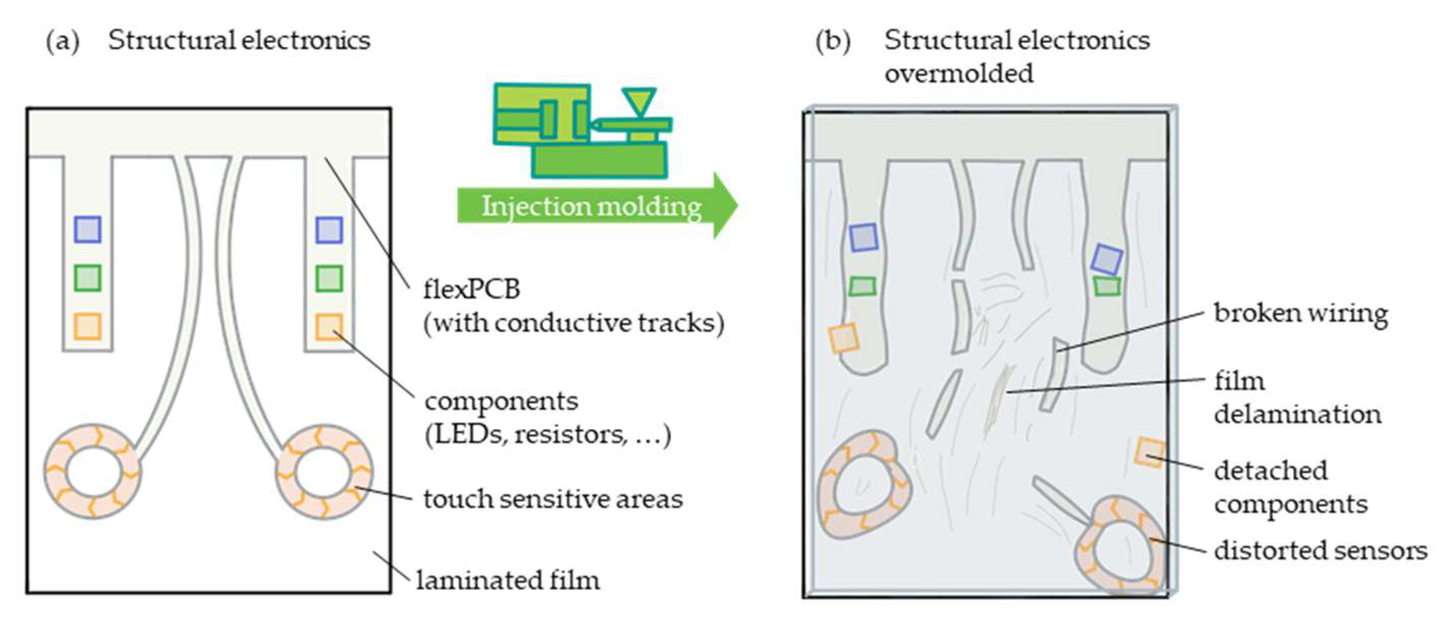
1. Introduction
2. Materials and Methods
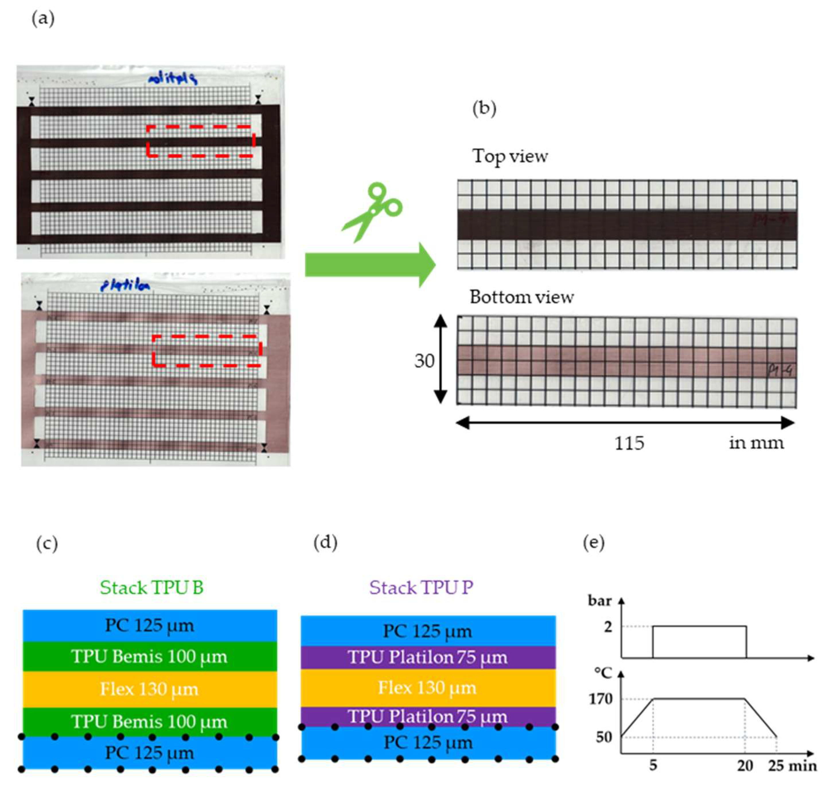
2.1. Film Design
2.2. Part Geometry and Molding Material
2.3. Injection Molding and Experimental Design
2.4. Molded Parts’ Analysis Procedure
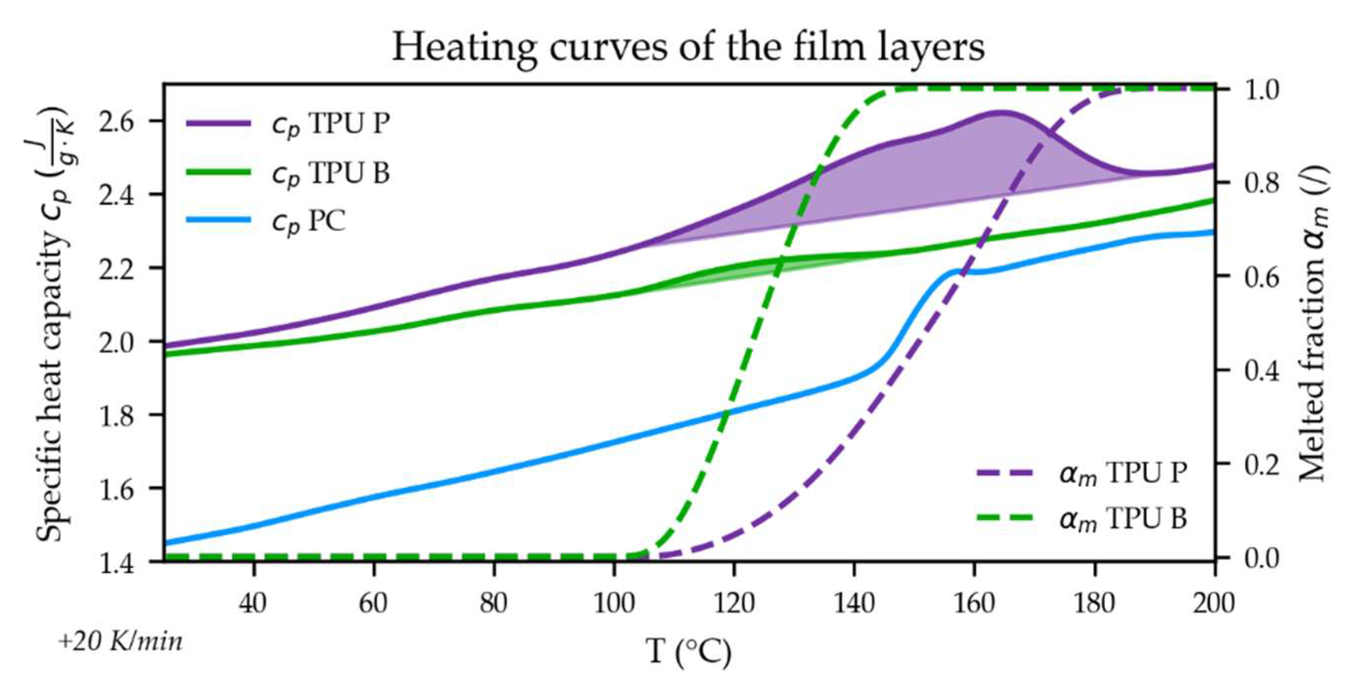
2.5. Simulation Model Preparation
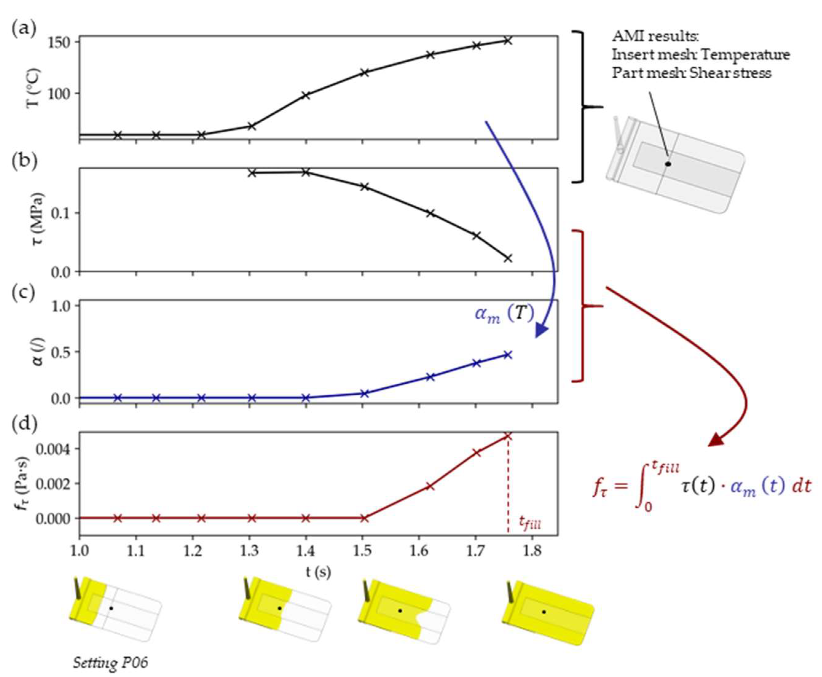
2.6. Simulation Analysis Procedure
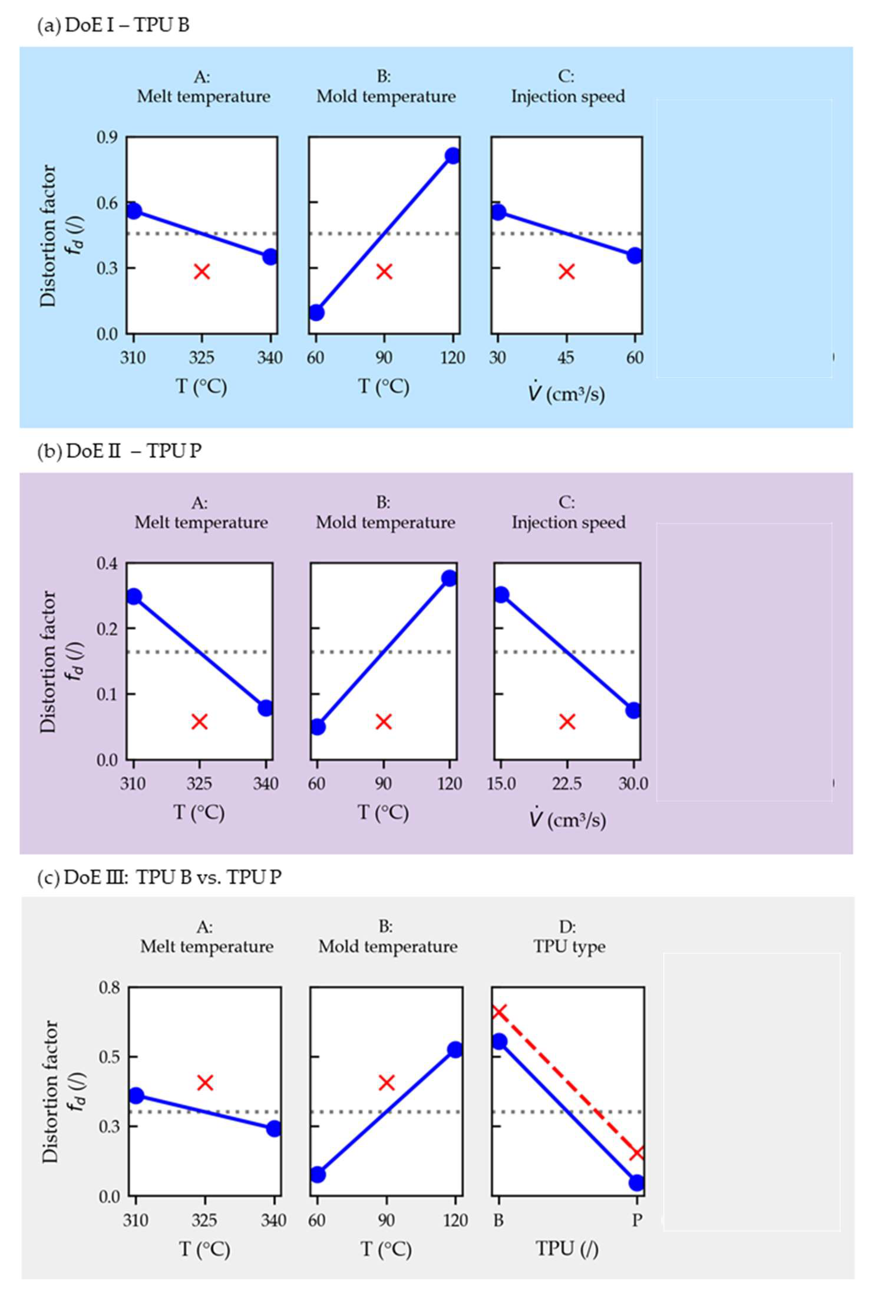
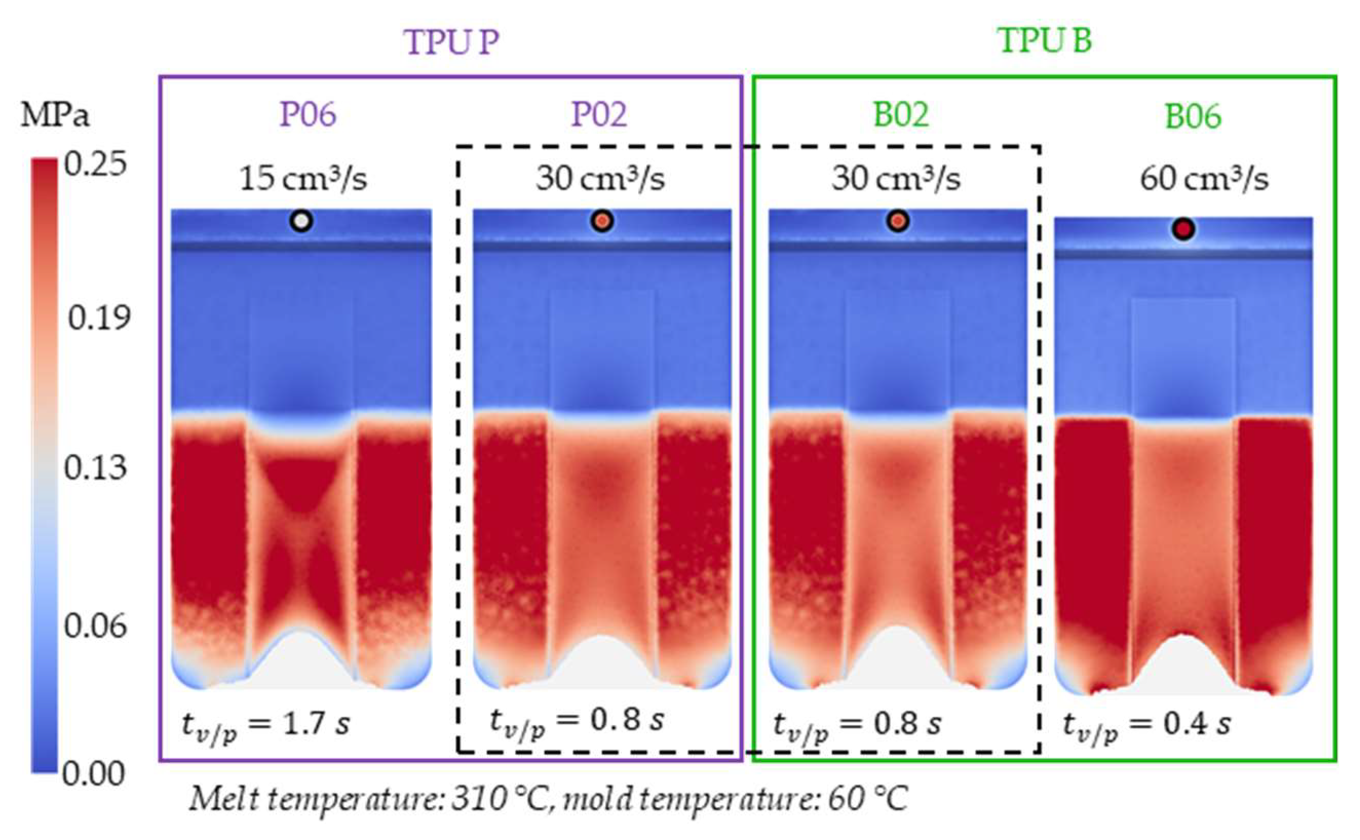
3. Results and Discussion
3.1. Characterization of Molded Parts
3.2. Analysis of Simulation
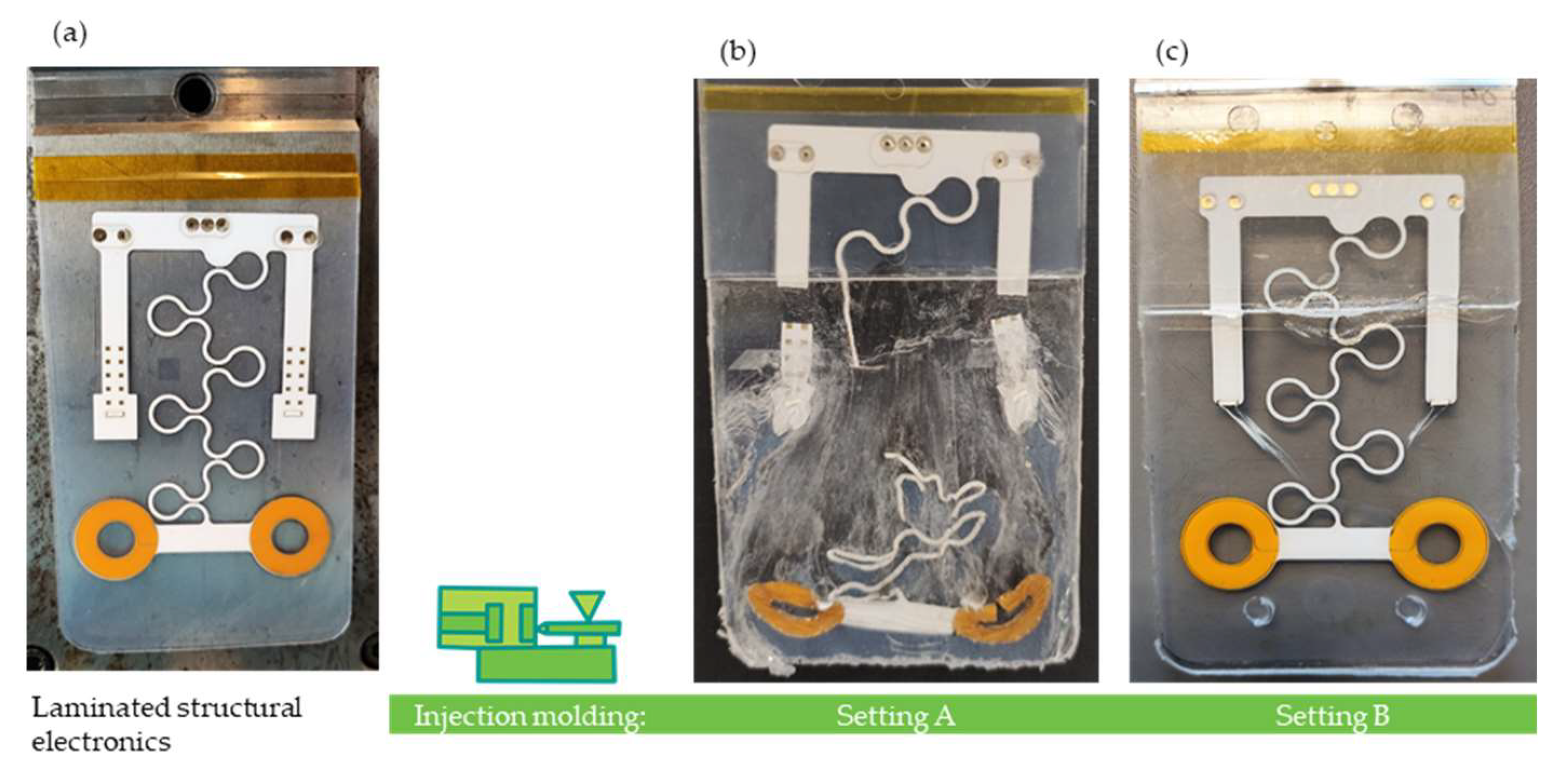
3.3. Demonstration
4. Conclusions
Author Contributions
Funding
Institutional Review Board Statement
Informed Consent Statement
Acknowledgments
Conflicts of Interest
References
- Beltrão, M.; Duarte, F.M.; Viana, J.C.; Paulo, V. A review on in-mold electronics technology. Polym. Eng. Sci. 2022, 62, 967–990. [Google Scholar] [CrossRef]
- Bakr, M.; Bossuyt, F.; Vanfleteren, J. The integration of electronic circuits in plastics using injection technologies: A literature review. Flex. Print. Electron. 2022, 7, 23001. [Google Scholar] [CrossRef]
- Simula, T.; Niskala, P.; Heikkinen, M.; Rusanen, O. Component Packages for IMSE™ (Injection Molded Structural Electronics). In Proceedings of the 2018 IMAPS Nordic Conference on Microelectronics Packaging (NordPac), Oulu, Finland, 12–14 June 2018; pp. 50–54. [Google Scholar]
- Rusanen, O.; Simula, T.; Niskala, P.; Lindholm, V.; Heikkinen, M. Injection Molded Structural Electronics Brings Surfaces to Life. In Proceedings of the 2019 22nd European Microelectronics and Packaging Conference & Exhibition (EMPC), Pisa, Italy, 16–19 September 2019; pp. 1–7. [Google Scholar]
- Isohätälä, A.; Sinivaara, H.; Heikkinen, M. Method for Manufacturing an Electronic Assembly and an Electronic Assembly. U.S. Patent 2018/0290356 A1, 18 October 2018. [Google Scholar]
- Ott, C.; Drummer, D. Low-stress over-molding of media-tight electronics using thermoplastic foam injection molding. Polym. Eng. Sci. 2021, 61, 1518–1528. [Google Scholar] [CrossRef]
- Vanfleteren, J.; Bossuyt, F.; Plovie, B. A new technology for rigid 3D free-form electronics based on the thermoplastic deformation of flat standard PCB type circuits. In Proceedings of the 2016 12th International Congress Molded Interconnect Devices (MID), Wuerzburg, Germany, 28–29 September 2016; pp. 1–4. [Google Scholar]
- Madadnia, B.; Bossuyt, F.; Vanfleteren, J. Technological development for the reduction of out-of-plane deformation of metallic meander structures in thermoformed electronics. Int. J. Adv. Manuf. Technol. 2022, 119, 6649–6663. [Google Scholar] [CrossRef]
- Välimäki, M.K.; Sokka, L.I.; Peltola, H.B.; Ihme, S.S.; Rokkonen, T.M.J.; Kurkela, T.J.; Ollila, J.T.; Korhonen, A.T.; Hast, J.T. Printed and hybrid integrated electronics using bio-based and recycled materials—Increasing sustainability with greener materials and technologies. Int. J. Adv. Manuf. Technol. 2020, 111, 325–339. [Google Scholar] [CrossRef]
- Kololuoma, T.; Pinheiro, C.; Kaisto, I.; Colley, A.; Ronka, K.; Keranen, M.; Kurkela, T.; Happonen, T.; Korkalainen, M.; Kehusmaa, M.; et al. Adopting Hybrid Integrated Flexible Electronics in Products: Case—Personal Activity Meter. IEEE J. Electron. Devices Soc. 2019, 7, 761–768. [Google Scholar] [CrossRef]
- Hsieh, L.Y.; Chang, K.-H. Yield improvement on in-mold decoration manufacturing through parameter optimization. Int. J. Precis. Eng. Manuf. 2013, 14, 1823–1828. [Google Scholar] [CrossRef]
- Chen, H.-L.; Chen, S.-C.; Liao, W.-H.; Chien, R.-D.; Lin, Y.-T. Effects of insert film on asymmetric mold temperature and associated part warpage during in-mold decoration injection molding of PP parts. Int. Commun. Heat Mass Transf. 2013, 41, 34–40. [Google Scholar] [CrossRef]
- Lin, Y.-H.; Chen, H.-L.; Chen, S.-C.; Lin, Y.-C. Effect of asymmetric cooling system on in-mold roller injection molded part warpage. Int. Commun. Heat Mass Transf. 2015, 61, 111–117. [Google Scholar] [CrossRef]
- Liu, S.-J.; Hsu, C.-M.; Chang, P.-W. Parameters Affecting the Ink Wash-off in In-mold Decoration of Injection Molded Parts. Int. Polym. Process. 2012, 27, 224–230. [Google Scholar] [CrossRef]
- Wielpütz, M. Analyse der Hinterspritztechnik Kompakter Dekormaterialien: = Analysis of the in-Mould Lamination Procecess with Compact Decoration Materials; Zugleich.: Aachen, Technische. Hochschule., Dissertation., 2003, 1. Auflage.; Druck- und Verlagshaus Mainz GmbH: Aachen, Germany, 2004; ISBN 3861304872. [Google Scholar]
- Woyan, F.; Koch, M.; Schneidmadel, S. Process Parameters Affecting the Quality of Functionalized in-Mold Decoration Injection Molded Composites. Ilmenau Scientific Colloquium. Available online: https://d-nb.info/1070667978/34 (accessed on 27 October 2022).
- Chen, S.-C.; Li, H.-M.; Huang, S.-T.; Wang, Y.-C. Effect of decoration film on mold surface temperature during in-mold decoration injection molding process. Int. Commun. Heat Mass Transf. 2010, 37, 501–505. [Google Scholar] [CrossRef]
- Lee, D.; Chen, W.-A.; Huang, T.-W.; Liu, S.-J. Factors Influencing the Warpage in In-Mold Decoration Injection Molded Composites. Int. Polym. Process. 2013, 28, 221–227. [Google Scholar] [CrossRef] [Green Version]
- Kleppmann, W. Versuchsplanung: Produkte und Prozesse Optimieren, 9th ed.; Überarbeitete Auflage; Hanser: Munich, Germany; Vienna, Austria, 2016; ISBN 3446447164. [Google Scholar]
- Autodesk Inc. 3D Flow Derivation|Moldflow Insight|Autodesk Knowledge Network. Available online: https://knowledge.autodesk.com/support/moldflow-insight/learn-explore/caas/CloudHelp/cloudhelp/2018/ENU/MoldflowInsight/files/GUID-C94D0362-421F-4EC1-89A6-931BB8D6D365-htm.html (accessed on 13 May 2022).
- Autodesk Inc. Synergy Application Programming Interface (API). Available online: https://help.autodesk.com/view/MFIA/2021/ENU/?guid=GUID-853E86EF-7294-424D-81AE-E38130C237A4 (accessed on 21 March 2022).
- The SciPy Community. Scipy.Integrate.Quad—SciPy v1.8.0 Manual. Available online: https://docs.scipy.org/doc/scipy/reference/generated/scipy.integrate.quad.html (accessed on 13 May 2022).


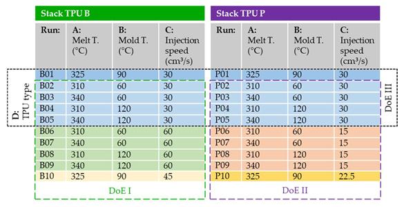
| Stack TPU B | ||||
| B01 325 °C / 90 °C / 30 cm³/s 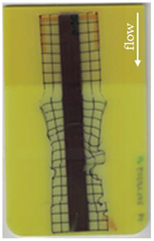 / III / III | B02 310 °C / 60 °C / 30 cm³/s 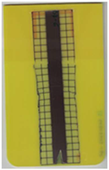 / II / II | B03 340 °C / 60 °C / 30 cm³/s 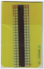 / I / I | B04 310 °C / 120 °C / 30 cm³/s  / III / III | B05 340 °C / 120 °C / 30 cm³/s 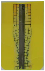 / III / III |
| B06 310 °C / 60 °C / 60 cm³/s  / I / I | B07 340 °C / 60 °C / 60 cm³/s 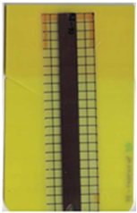 / I / I | B08 310 °C / 120 °C / 60 cm³/s 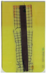 / III / III | B09 340 °C / 120 °C / 60 cm³/s 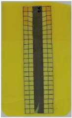 / II / II | B10 325 °C / 90 °C / 45 cm³/s 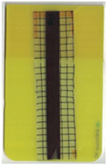 / II / II |
| Stack TPU P | ||||
| P01 325 °C / 90°C / 30 cm³/s 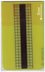 / I / I | P02 310 °C / 60 °C / 30 cm³/s 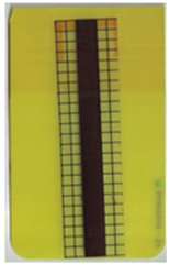 / I / I | P03 340 °C / 60 °C / 30 cm³/s 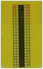 / I / I | P04 310 °C / 120 °C / 30 cm³/s 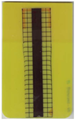 / II / II | P05 340 °C / 120 °C / 30 cm³/s  0.08 / I 0.08 / I |
| P06 310 °C / 60 °C / 15 cm³/s 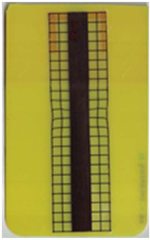 0.19 / II 0.19 / II | P07 340 °C / 60 °C / 15 cm³/s 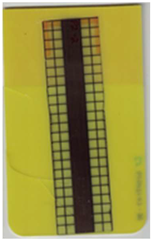 / I / I | P08 310 °C / 120 °C / 15 cm³/s 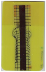 / III / III | P09 340 °C / 120 °C / 15 cm³/s 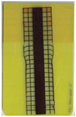 / II / II | P10 325 °C / 90 °C / 22.5 cm³/s 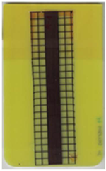 / I / I |
| Distortion Factors (fd): | |||
|---|---|---|---|
| DoE I: Stack TPU B | |||
| p-values for coefficients: |
| ||
| Regression: | |||
| R2: | 94% | R2adj.: | 93% |
| DoE II: Stack TPU P | |||
| p-values for coefficients: |
| ||
| Regression: | |||
| R2: | 81% | R2adj.: | 78% |
| DoE III: Stack TPU B and TPU P at injection speed 30 cm3/s | |||
| p-values for coefficients: |
| ||
| Regression: | |||
| R2: | 83% | R2adj.: | 80% |
| Stack TPU B | ||||
| B01 325 °C / 90 °C / 30 cm³/s 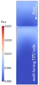 | B02 310 °C / 60 °C / 30 cm³/s  | B03 340 °C / 60 °C / 30 cm³/s  | B04 310 °C / 120 °C / 30 cm³/s  | B05 340 °C / 120 °C / 30 cm³/s  |
| B06 310 °C / 60 °C / 60 cm³/s  | B07 340 °C / 60 °C / 60 cm³/s  | B08 310 °C / 120 °C / 60 cm³/s  | B09 340 °C / 120 °C / 60 cm³/s  | B10 325 °C / 90 °C / 45 cm³/s  |
| Stack TPU P | ||||
| P01 325 °C / 90 °C / 30 cm³/s 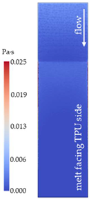 | P02 310 °C / 60 °C / 30 cm³/s  | P03 340 °C / 60 °C / 30 cm³/s  | P04 310 °C / 120 °C / 30 cm³/s  | P05 340 °C / 120 °C / 30 cm³/s  |
| P06 310 °C / 60 °C / 15 cm³/s  | P07 340 °C / 60 °C / 15 cm³/s  | P08 310 °C / 120 °C / 15 cm³/s  | P09 340 °C / 120 °C / 15 cm³/s  | P10 325 °C / 90 °C / 22.5 cm³/s  |
| Averaged Shear Distortion Factor (): | |||
|---|---|---|---|
| DoE I: Stack TPU B | |||
| Factors: |
| ||
| Regression: | |||
| R2: | 95.33% | R2adj.: | 87.55% |
| DoE II: Stack TPU P | |||
| Factors: |
| ||
| Regression: | |||
| R2: | 94.48% | R2adj.: | 85.28% |
| DoE III: Stack TPU B and TPU P at injection speed 30 cm3/s | |||
| Factors: |
| ||
| Regression: | |||
| R2: | 93.35% | R2adj.: | 85.03% |
| Melt Temperature (°C) | Mold Temperature (°C) | Injection Speed (cm3/s) | TPU Type (/) | |
|---|---|---|---|---|
| Setting A | 310 | 120 | 30 | B |
| Setting B | 340 | 120 | 60 | P |
Publisher’s Note: MDPI stays neutral with regard to jurisdictional claims in published maps and institutional affiliations. |
© 2022 by the authors. Licensee MDPI, Basel, Switzerland. This article is an open access article distributed under the terms and conditions of the Creative Commons Attribution (CC BY) license (https://creativecommons.org/licenses/by/4.0/).
Share and Cite
Hubmann, M.; Madadnia, B.; Groten, J.; Pletz, M.; Vanfleteren, J.; Stadlober, B.; Bossuyt, F.; Kaur, J.; Lucyshyn, T. Process Optimization of Injection Overmolding Structural Electronics with Regard to Film Distortion. Polymers 2022, 14, 5060. https://doi.org/10.3390/polym14235060
Hubmann M, Madadnia B, Groten J, Pletz M, Vanfleteren J, Stadlober B, Bossuyt F, Kaur J, Lucyshyn T. Process Optimization of Injection Overmolding Structural Electronics with Regard to Film Distortion. Polymers. 2022; 14(23):5060. https://doi.org/10.3390/polym14235060
Chicago/Turabian StyleHubmann, Martin, Behnam Madadnia, Jonas Groten, Martin Pletz, Jan Vanfleteren, Barbara Stadlober, Frederick Bossuyt, Jatinder Kaur, and Thomas Lucyshyn. 2022. "Process Optimization of Injection Overmolding Structural Electronics with Regard to Film Distortion" Polymers 14, no. 23: 5060. https://doi.org/10.3390/polym14235060