
Design of a Structure for Optimized Optical Performance of a Full Colored Organic Light-Emitting Diode on a Parameter Space Map

 and
and 
Abstract
:1. Introduction
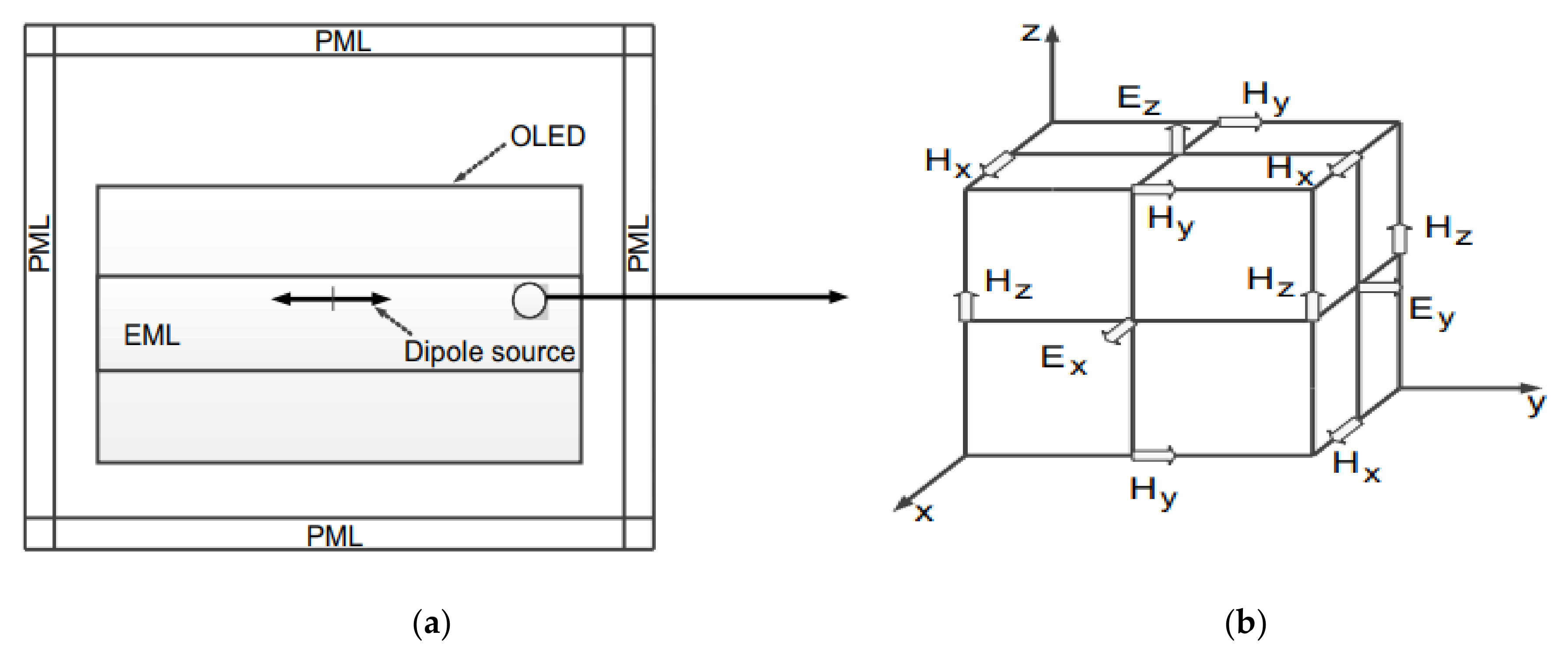
2. Method
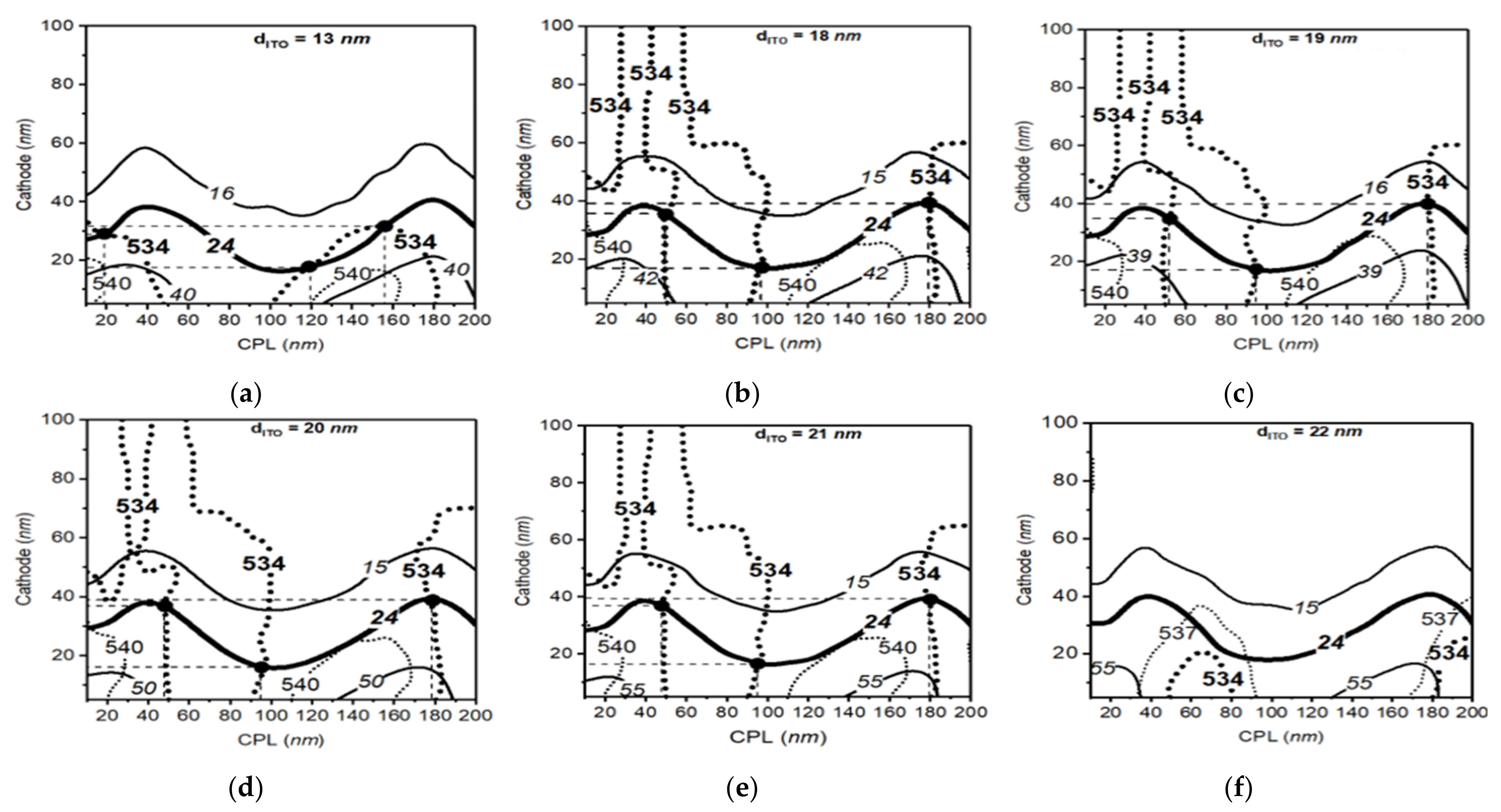
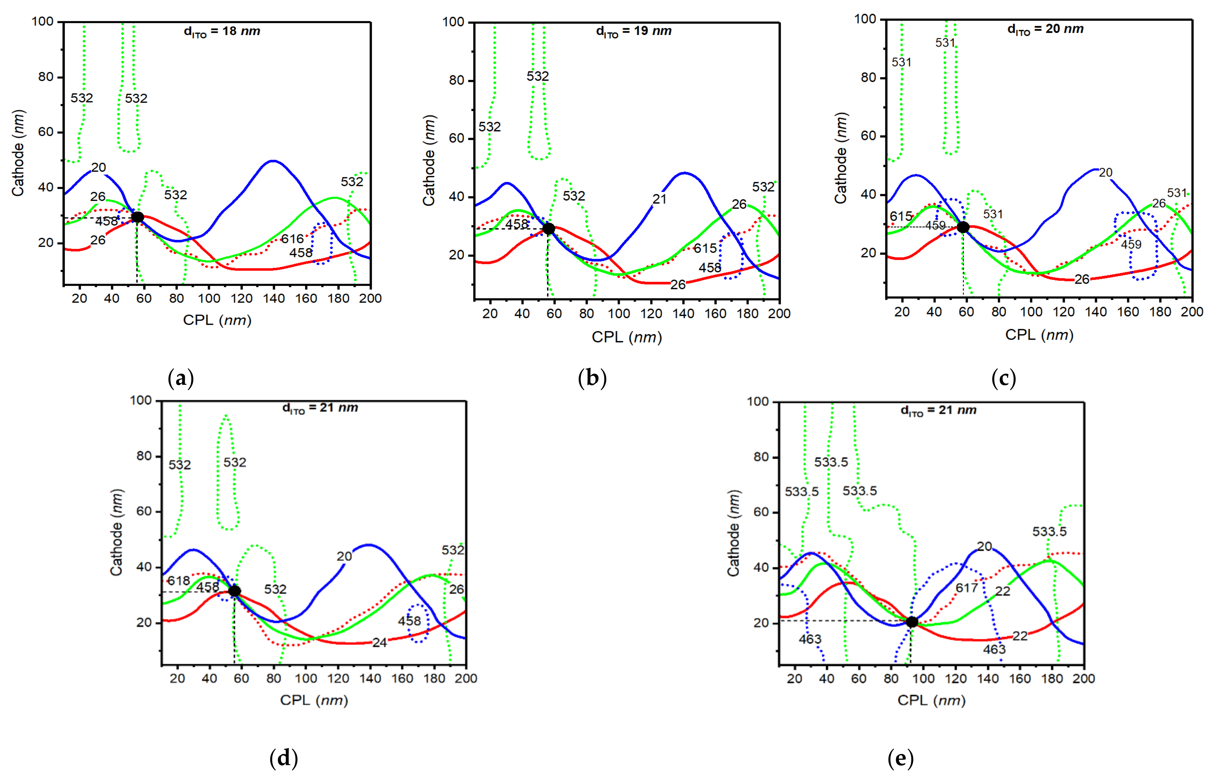
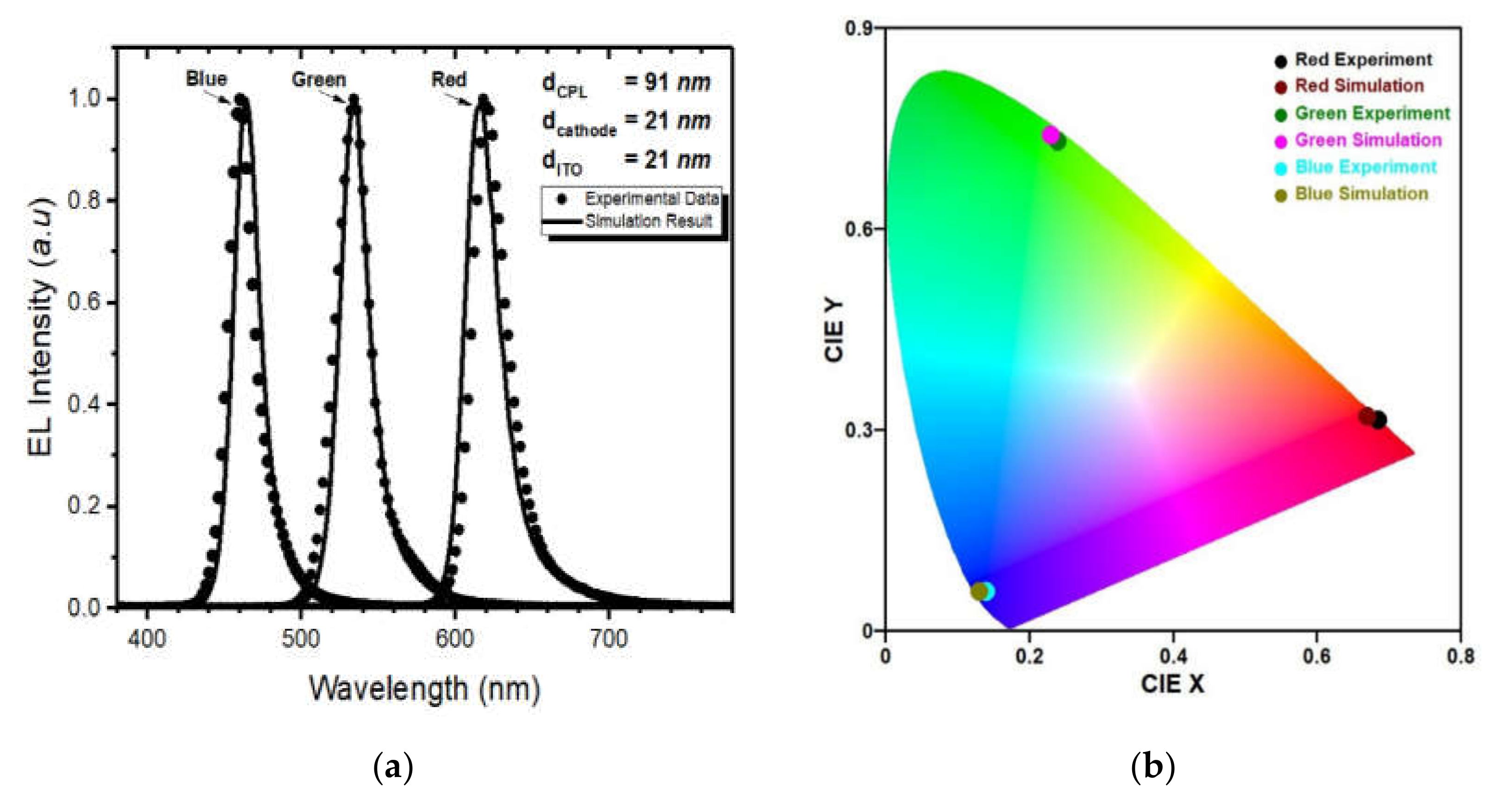
3. Results
4. Conclusions
Author Contributions
Funding
Institutional Review Board Statement
Informed Consent Statement
Data Availability Statement
Conflicts of Interest
References
- Reineke, S.; Linder, F.; Schwartz, G.; Seidler, N.; Walzer, K.; Lüssem, B.; Leo, K. White organic light-emitting diodes with fluorescent tube efficiency. Nature 2009, 459, 234–238. [Google Scholar] [CrossRef] [PubMed]
- Krotkus, S.; Kasemann, D.; Lenk, S.; Leo, K.; Reineke, S. Adjustable white-light emission from a photo-structured micro-OLED array. Light Sci. Appl. 2016, 5, e16121. [Google Scholar] [CrossRef] [PubMed] [Green Version]
- Su, S.-J.; Gonmori, E.; Sasabe, H.; Kido, J. Highly Efficient Organic Blue-and White-Light-Emitting Devices Having a Carrier- and Exciton-Confining Structure for Reduced Efficiency Roll-Off. Adv. Mater. 2008, 20, 4189–4194. [Google Scholar] [CrossRef]
- Zhu, X.; Sun, J.; Yu, X.; Wong, M.; Kwok, H.-S. High-Performance Top-Emitting White Organic Light-Emitting Devices. Jpn. J. Appl. Phys. 2007, 46, 4054–4058. [Google Scholar] [CrossRef]
- Luo, D.; Chen, Q.; Liu, B.; Qiu, Y. Emergence of Flexible White Organic Light-Emitting Diodes. Polymers 2019, 11, 384. [Google Scholar] [CrossRef] [Green Version]
- Chen, L.-Y.; Hsieh, K.-M.; Wu, Y.-J.; Hsieh, C.-A.; Chang, J.-K.; Liu, D.-H.; Hung, H.-W.; Ho, S.-Y.; Chang, C.-H. Novel scattering and color converting substrates for simple-structured white organic light-emitting diodes. Org. Electron. 2021, 89, 106045. [Google Scholar] [CrossRef]
- Chen, H.-W.; Lee, J.-H.; Lin, B.-Y.; Chen, S.; Wu, S.-T. Liquid crystal display and organic light-emitting diode display: Present status and future perspectives. Light Sci. Appl. 2018, 7, 17168. [Google Scholar] [CrossRef]
- Tang, X.; Liu, X.-Y.; Jiang, Z.-Q.; Liao, L.-S. High-Quality White Organic Light-Emitting Diodes Composed of Binary Emitters with Color Rendering Index Exceeding 80 by Utilizing Color Remedy Strategy. Adv. Funct. Mater. 2019, 29, 1807541. [Google Scholar] [CrossRef]
- Zhang, H.; Xue, J.; Li, C.; Zhang, S.; Yang, B.; Liu, Y.; Wang, Y. Novel Deep-Blue Hybridized Local and Charge-Transfer host Emitter for High-Quality Fluorescence/Phosphor Hybrid Quasi-White Organic Light-Emitting Diode. Adv. Funct. Mater. 2021, 31, 2100704. [Google Scholar] [CrossRef]
- Raychaudhuri, P.K.; Madathil, J.K.; Shore, J.D.; Van, S.A. Performance enhancement of top- and bottom-emitting organic light-emitting devices using microcavity structures. J. Soc. Inf. Disp. 2004, 12, 315–321. [Google Scholar] [CrossRef]
- Hsu, S.F.; Lee, C.-C.; Hu, A.T.; Chen, C.H. Fabrication of blue top-emitting organic light-emitting devices with highly saturated color. Curr. Appl. Phys. 2004, 4, 663–666. [Google Scholar] [CrossRef]
- Kwon, S.-K.; Lee, E.-H.; Kim, K.-S.; Choi, H.-C.; Park, M.J.; Kim, S.K.; Pode, R.; Kwon, J.H. Efficient micro-cavity top emission OLED with optimized Mg:Ag ratio cathode. Opt. Express 2017, 25, 29906–29915. [Google Scholar] [CrossRef] [PubMed]
- Wu, Z.; Zhai, Y.; Guo, R.; Wang, J. Red top-emitting organic light-emitting device with improved efficiency and saturated color. J. Lumin. 2011, 131, 2042–2045. [Google Scholar] [CrossRef]
- Kashiwabara, M.; Hanawa, K.; Asaki, R.; Kobori, I.; Matsuura, R.; Yamada, H.; Yamamoto, T.; Ozawa, A.; Sato, Y.; Terada, S.; et al. Late-News Paper: Advanced AM-OLED Display Based on White Emitter with Microcavity Structure. SID Symp. Dig. Tech. Pap. 2012, 35, 1017–1019. [Google Scholar] [CrossRef]
- Yokoyama, D.; Sasaki, T.; Suzuki, Y.; Abe, T.; Tsuruoka, K.; Miyajima, T.; Kakiuchi, T.; Morita, C.; Aoki, M.; Ouchi, Y.; et al. Active refractive index control using a stably evaporable perfluororesin for high-outcoupling-efficiency organic light-emitting diodes. J. Mater. Chem. C. 2021, 9, 11115–11125. [Google Scholar] [CrossRef]
- Chen, S.; Deng, L.; Xie, J.; Peng, L.; Xie, L.; Fan, Q.; Huang, W. Recent Developments in Top-Emitting Organic Light-Emitting Diodes. Adv. Mater. 2010, 22, 5227–5239. [Google Scholar] [CrossRef]
- Cao, J.; Liu, X.; Khan, M.A.; Zhu, W.; Jiang, X.; Zhang, Z.; Xu, S. RGB tricolor produced by white-based top-emitting organic light-emitting diodes with microcavity structure. Curr. Appl. Phys. 2007, 7, 300–304. [Google Scholar] [CrossRef]
- Thomschke, M.; Nitsche, R.; Furno, M.; Leo, K. Optimized efficiency and angular emission characteristics of white top-emitting organic electroluminescent diodes. Appl. Phys. Lett. 2009, 94, 083303. [Google Scholar] [CrossRef]
- Kim, S.; Park, M.; Pode, R.; Kwon, J. A Deep Blue Strong Microcavity Organic Light-Emitting Diode Optimized by a Low Absorption Semitransparent Cathode and a Narrow Bandwidth Emitter. Adv. Photonics Res. 2021, 2, 2000122. [Google Scholar] [CrossRef]
- Tran, A.D.; Le, V.D.; Kang, B.; Lee, G.-D.; Choi, H. Investigation of the Optical Performance of an Organic Light-Emitting Diode on a Parameter Space Map for Desired Color Performance. J. Korean Phys. Soc. 2019, 75, 126–130. [Google Scholar] [CrossRef]
- Peckham, J.; Cheng, J.; Ward, A.; Campbell, J.; Krause, K.; Bachman, D.; Rutledge, S.; Biswas, T.; Mohammadpour, A.; Haas, W. Optimization of OLED Microcavity Design and Fabrication for Light Field Display. SID Symp. Dig. Tech. Pap. 2018, 49, 1785–1788. [Google Scholar] [CrossRef]
- Sullivan, D.; Liu, J.; Kuzyk, M. Three-Dimensional Optical Pulse Simulation Using the FDTD method. IEEE Trans. Microw. Theory Tech. 2000, 48, 1127–1133. [Google Scholar] [CrossRef]
- Oh, C.; Escuti, M.J. Time domain analysis of periodic anisotropic media at oblique incidence: An efficient FDTD implementation. Opt. Express 2006, 14, 11870–11884. [Google Scholar] [CrossRef] [PubMed]
- Callens, M.K.; Marsman, H.; Penninck, L.; Peeters, P.; Groot, H.D.; Meulen, J.M.; Neyts, K. RCWA and FDTD modeling of light emission from internally structured OLEDs. Opt. Express 2014, 22, A589–A600. [Google Scholar] [CrossRef] [PubMed]
- Oskooi, A.F.; Roundy, D.; Ibanescu, M.; Bermel, P.; Joannopoulos, J.D.; Johnson, S.G. Meep: A flexible free-software package for electromagnetic simulations by the FDTD method. Comput. Phys. Commun. 2010, 181, 687–702. [Google Scholar] [CrossRef]
- Juntunen, J.S.; Tsiboukis, T.D. Reduction of Numerical Dispersion in FDTD method Through Artificial Anisotropy. IEEE Trans. Microw. Theory Tech. 2000, 48, 582–588. [Google Scholar] [CrossRef] [Green Version]
- Kim, K.-H.; Kim, J.-J. Origin and Control of Orientation of phosphorescent and TADF Dyes for High-Efficiency OLEDs. Adv. Mater. 2018, 18, 1705600. [Google Scholar] [CrossRef]
- Mann, V.; Rastogi, V. Dielectric nanoparticles for the enhancement of OLED light extraction efficiency. Opt. Commun. 2017, 387, 202–207. [Google Scholar] [CrossRef]


| Layers | Thickness | Refractive | Extinction | Refractive | Extinction |
|---|---|---|---|---|---|
| HTL | 93 nm | 1.85505 | 0 | 1.63631 | 0 |
| R Prime | 68 nm | 1.86839 | 1.67377 | 0.00181 | |
| pHTL | 9 nm | 1.86117 | 0 | 1.65279 | 0 |
| Layers | Thickness | Refractive Index | Extinction Coefficient |
|---|---|---|---|
| CPL | Varied | 1.92392 | 0 |
| Cathode | Varied | 1.2068 | 0 |
| Cathode 1 | 3 | 0.175646 | 2.76587 |
| ETL | 30 | 1.84152 | |
| R-EML | 15 | 2.04304 | |
| G-EML | 15 | 1.95648 | |
| B-EML | 15 | 1.84815 | 0 |
| EBL | 15 | 1.81139 | |
| G Prime | 40 | 1.97543 | 0 |
| ITO | Varied | 2.0227 | |
| Anode | 1000 | 0.14579 | 3.2904 |
Publisher’s Note: MDPI stays neutral with regard to jurisdictional claims in published maps and institutional affiliations. |
© 2022 by the authors. Licensee MDPI, Basel, Switzerland. This article is an open access article distributed under the terms and conditions of the Creative Commons Attribution (CC BY) license (https://creativecommons.org/licenses/by/4.0/).
Share and Cite
Lee, C.-H.; Choi, J.-H.; Hyun, S.-Y.; Baek, J.-H.; Kang, B.; Lee, G.-D. Design of a Structure for Optimized Optical Performance of a Full Colored Organic Light-Emitting Diode on a Parameter Space Map. Polymers 2022, 14, 585. https://doi.org/10.3390/polym14030585
Lee C-H, Choi J-H, Hyun S-Y, Baek J-H, Kang B, Lee G-D. Design of a Structure for Optimized Optical Performance of a Full Colored Organic Light-Emitting Diode on a Parameter Space Map. Polymers. 2022; 14(3):585. https://doi.org/10.3390/polym14030585
Chicago/Turabian StyleLee, Chang-Hee, Ju-Hyeok Choi, Seo-Yong Hyun, Ji-Ho Baek, Bongsoon Kang, and Gi-Dong Lee. 2022. "Design of a Structure for Optimized Optical Performance of a Full Colored Organic Light-Emitting Diode on a Parameter Space Map" Polymers 14, no. 3: 585. https://doi.org/10.3390/polym14030585
APA StyleLee, C.-H., Choi, J.-H., Hyun, S.-Y., Baek, J.-H., Kang, B., & Lee, G.-D. (2022). Design of a Structure for Optimized Optical Performance of a Full Colored Organic Light-Emitting Diode on a Parameter Space Map. Polymers, 14(3), 585. https://doi.org/10.3390/polym14030585