
Analysis of Diffracted Mode Outcoupling in the Context of Amplified Spontaneous Emission of Organic Thin Films


Abstract
:1. Introduction
2. Experimental Section
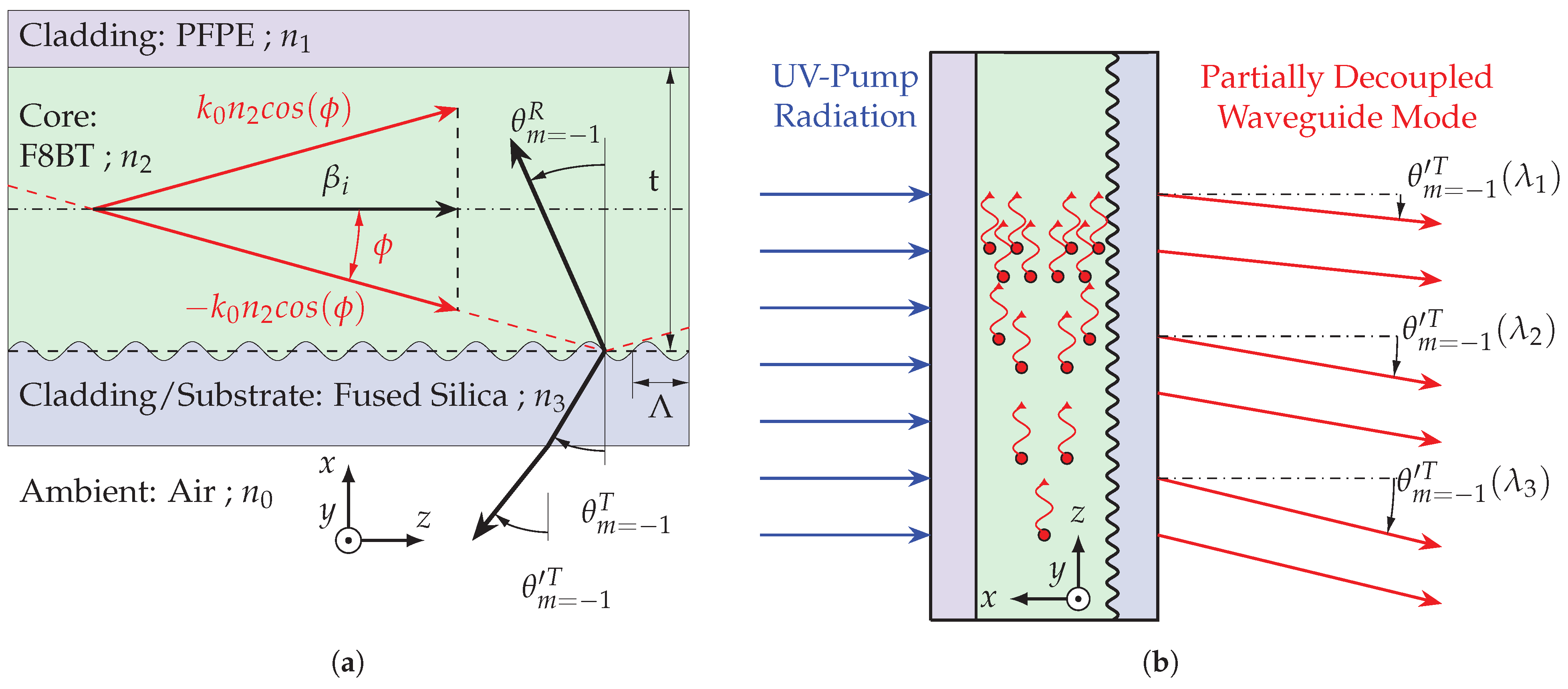
2.1. Sample Design
2.2. Fabrication
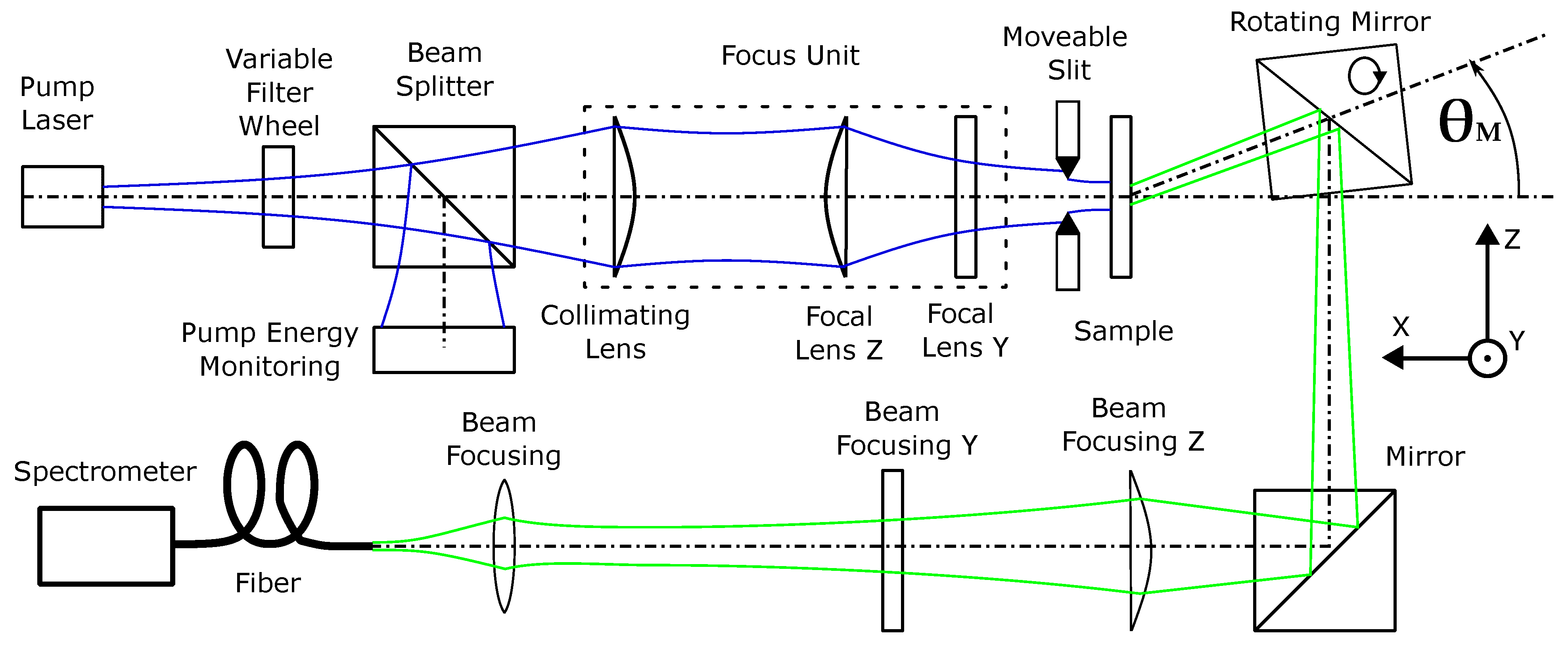
2.3. Optical Setup
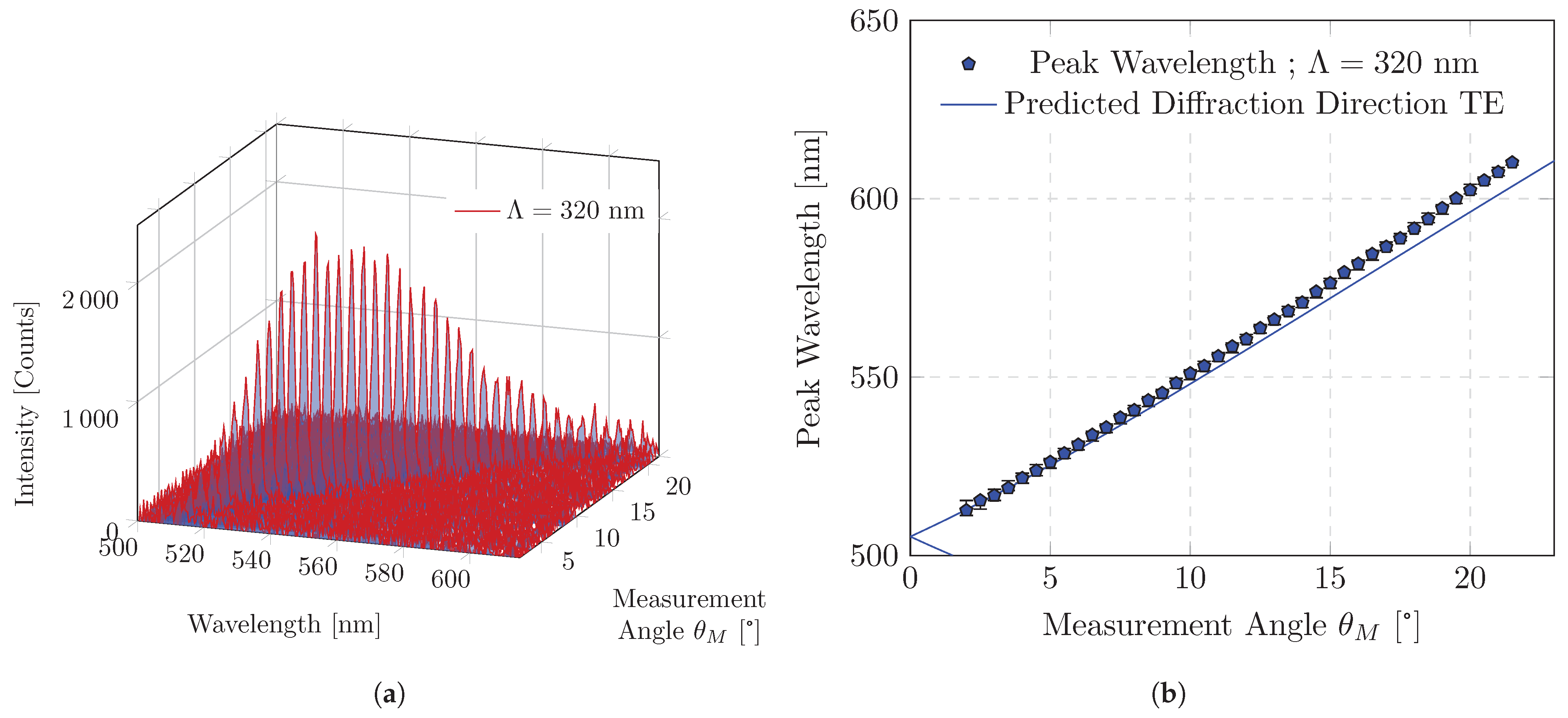
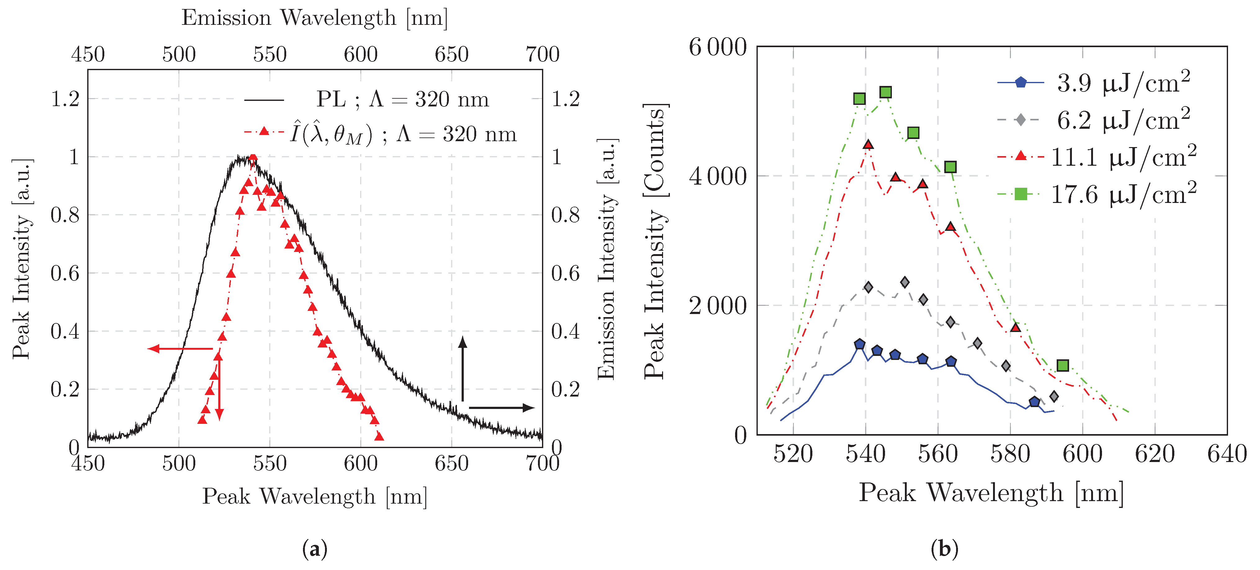
3. Results
3.1. Diffraction Direction and Surface Emission Spectrum
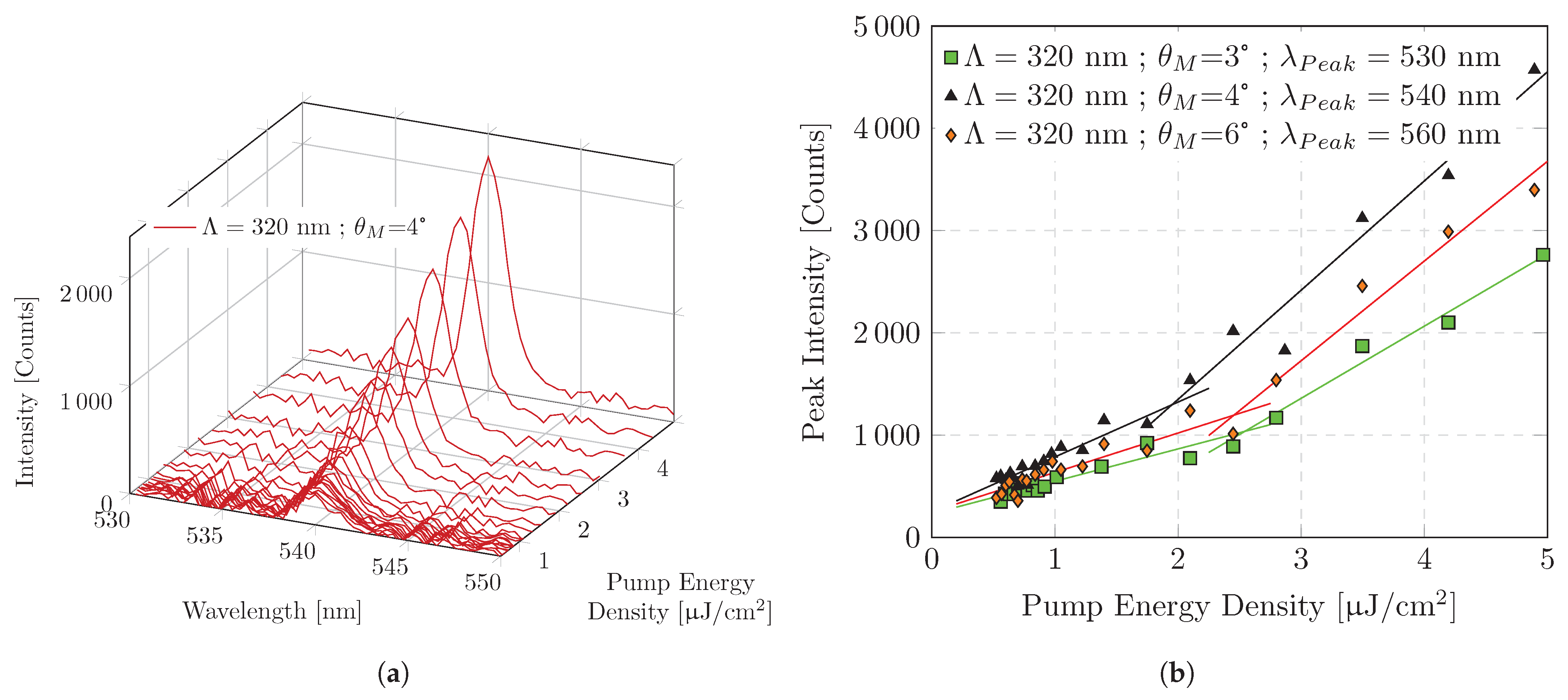
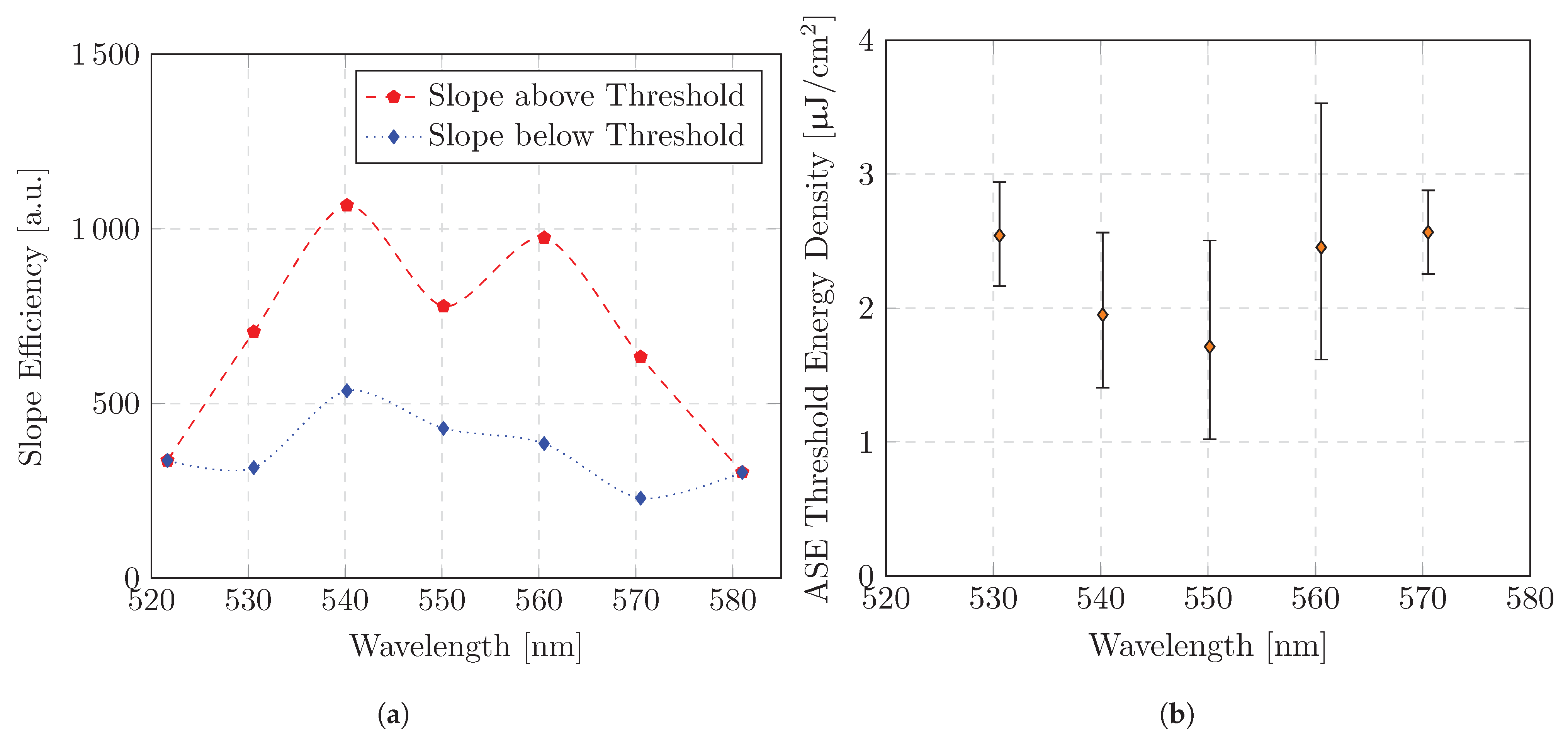
3.2. ASE Threshold
4. Discussion
5. Conclusions
Author Contributions
Funding
Institutional Review Board Statement
Data Availability Statement
Conflicts of Interest
Appendix A. Refractive Index F8BT

| Periodicity | Bragg Wavelength | Reffractive Index |
|---|---|---|
| Λ [nm] | [nm] | |
| 330 | 516 | 1.7883 |
| 340 | 527.9 | 1.7781 |
| 350 | 540.4 | 1.7706 |
| 360 | 553.1 | 1.7648 |
| 370 | 566.1 | 1.7606 |
| 380 | 580.4 | 1.7630 |
References
- Moses, D. High quantum efficiency luminescence from a conducting polymer in solution: A novel polymer laser dye. Appl. Phys. Lett. 1992, 60, 3215–3216. [Google Scholar] [CrossRef]
- Hide, F.; Díaz-García, M.A.; Schwartz, B.J.; Andersson, M.R.; Pei, Q.; Heeger, A.J. Semiconducting Polymers: A New Class of Solid-State Laser Materials. Science 1996, 273, 1833–1836. [Google Scholar] [CrossRef]
- Kuehne, A.J.C.; Gather, M.C. Organic Lasers: Recent Developments on Materials, Device Geometries, and Fabrication Techniques. Chem. Rev. 2016, 116, 12823–12864. [Google Scholar] [CrossRef]
- Chénais, S.; Forget, S. Recent advances in solid-state organic lasers. Polym. Int. 2011, 61, 390–406. [Google Scholar] [CrossRef]
- Xia, H.; Hu, C.; Chen, T.; Hu, D.; Zhang, M.; Xie, K. Advances in Conjugated Polymer Lasers. Polymers 2019, 11, 443. [Google Scholar] [CrossRef]
- Karnutsch, C.; Pflumm, C.; Heliotis, G.; deMello, J.C.; Bradley, D.D.C.; Wang, J.; Weimann, T.; Haug, V.; Gärtner, C.; Lemmer, U. Improved organic semiconductor lasers based on a mixed-order distributed feedback resonator design. Appl. Phys. Lett. 2007, 90, 131104. [Google Scholar] [CrossRef]
- Shankarling, G.S.; Jarag, K.J. Laser dyes. Resonance 2010, 15, 804–818. [Google Scholar] [CrossRef]
- Samuel, I.D.W.; Turnbull, G.A. Organic Semiconductor Lasers. Chem. Rev. 2007, 107, 1272–1295. [Google Scholar] [CrossRef] [PubMed]
- Clark, J.; Lanzani, G. Organic photonics for communications. Nat. Photonics 2010, 4, 438–446. [Google Scholar] [CrossRef]
- Klinkhammer, S.; Liu, X.; Huska, K.; Shen, Y.; Vanderheiden, S.; Valouch, S.; Vannahme, C.; Bräse, S.; Mappes, T.; Lemmer, U. Continuously tunable solution-processed organic semiconductor DFB lasers pumped by laser diode. Opt. Express 2012, 20, 6357. [Google Scholar] [CrossRef]
- Scherf, U.; Riechel, S.; Lemmer, U.; Mahrt, R. Conjugated polymers: Lasing and stimulated emission. Curr. Opin. Solid State Mater. Sci. 2001, 5, 143–154. [Google Scholar] [CrossRef]
- McGehee, M.D.; Heeger, A.J. Semiconducting (conjugated) polymers as materials for solid-state lasers. Adv. Mater. 2000, 12, 1655–1668. [Google Scholar] [CrossRef]
- Lippi, G.L. “Amplified Spontaneous Emission” in Micro- and Nanolasers. Atoms 2021, 9, 6. [Google Scholar] [CrossRef]
- Milanese, S.; De Giorgi, M.L.; Anni, M. Determination of the Best Empiric Method to Quantify the Amplified Spontaneous Emission Threshold in Polymeric Active Waveguides. Molecules 2020, 25, 2992. [Google Scholar] [CrossRef]
- Lattante, S.; Cretí, A.; Lomascolo, M.; Anni, M. On the correlation between morphology and Amplified Spontaneous Emission properties of a polymer: Polymer blend. Org. Electron. 2016, 29, 44–49. [Google Scholar] [CrossRef]
- Liu, X.; Py, C.; Tao, Y.; Li, Y.; Ding, J.; Day, M. Low-threshold amplified spontaneous emission and laser emission in a polyfluorene derivative. Appl. Phys. Lett. 2004, 84, 2727–2729. [Google Scholar] [CrossRef]
- Wilke, H.; Hoinka, N.M.; Kusserow, T.; Fuhrmann-Lieker, T.; Hillmer, H. Determination of the saturation length and study of its effects in optical gain measurements of organic semiconductors using the variable stripe length method. Appl. Phys. Lett. 2019, 115, 173301. [Google Scholar] [CrossRef]
- Cerdán, L.; Costela, A.; García-Moreno, I. On the characteristic lengths in the variable stripe length method for optical gain measurements. J. Opt. Soc. Am. B 2010, 27, 1874. [Google Scholar] [CrossRef]
- McGehee, M.D.; Gupta, R.; Veenstra, S.; Miller, E.K.; Díaz-García, M.A.; Heeger, A.J. Amplified spontaneous emission from photopumped films of a conjugated polymer. Phys. Rev. B 1998, 58, 7035–7039. [Google Scholar] [CrossRef]
- Cerdán, L. Variable Stripe Length method: Influence of stripe length choice on measured optical gain. Opt. Lett. 2017, 42, 5258. [Google Scholar] [CrossRef]
- Gozhyk, I.; Boudreau, M.; Haghighi, H.R.; Djellali, N.; Forget, S.; Chénais, S.; Ulysse, C.; Brosseau, A.; Pansu, R.; Audibert, J.F.; et al. Gain properties of dye-doped polymer thin films. Phys. Rev. B 2015, 92, 214202. [Google Scholar] [CrossRef]
- Wang, Y.H.; Peng, Y.J.; Mo, Y.Q.; Yang, Y.Q.; Zheng, X.X. Analysis on the mechanism of photoluminescence quenching in pi-conjugated polymers in photo-oxidation process with broadband transient grating. Appl. Phys. Lett. 2008, 93, 231902. [Google Scholar] [CrossRef]
- Hale, G.D.; Oldenburg, S.J.; Halas, N.J. Effects of photo-oxidation on conjugated polymer films. Appl. Phys. Lett. 1997, 71, 1483–1485. [Google Scholar] [CrossRef]
- Pudleiner, T.; Sutter, E.; Knyrim, J.; Karnutsch, C. Colorimetric Phosphate Detection Using Organic DFB Laser Based Absorption Spectroscopy. Micromachines 2021, 12, 1492. [Google Scholar] [CrossRef] [PubMed]
- Yang, Y.; Turnbull, G.A.; Samuel, I.D.W. Hybrid optoelectronics: A polymer laser pumped by a nitride light-emitting diode. Appl. Phys. Lett. 2008, 92, 163306. [Google Scholar] [CrossRef]
- Annavarapu, N.; Goldberg, I.; Papadopoulou, A.; Elkhouly, K.; Genoe, J.; Gehlhaar, R.; Heremans, P. Scattered Emission Profile Technique for Accurate and Fast Assessment of Optical Gain in Thin Film Lasing Materials. ACS Photonics 2023, 10, 1583–1590. [Google Scholar] [CrossRef]
- Turnbull, G.A.; Andrew, P.; Jory, M.J.; Barnes, W.L.; Samuel, I.D.W. Relationship between photonic band structure and emission characteristics of a polymer distributed feedback laser. Phys. Rev. B 2001, 64, 125122. [Google Scholar] [CrossRef]
- Safonov, A.; Jory, M.; Matterson, B.; Lupton, J.; Salt, M.; Wasey, J.; Barnes, W.; Samuel, I. Modification of polymer light emission by lateral microstructure. Synth. Met. 2001, 116, 145–148. [Google Scholar] [CrossRef]
- Yariv, A.; Nakamura, M. Periodic structures for integrated optics. IEEE J. Quantum Electron. 1977, 13, 233–253. [Google Scholar] [CrossRef]
- Amarasinghe, D.; Ruseckas, A.; Vasdekis, A.E.; Turnbull, G.A.; Samuel, I.D.W. High-Gain Broadband Solid-State Optical Amplifier using a Semiconducting Copolymer. Adv. Mater. 2009, 21, 107–110. [Google Scholar] [CrossRef]
- Kogelnik, H.; Shank, C.V. Coupled-Wave Theory of Distributed Feedback Lasers. J. Appl. Phys. 1972, 43, 2327–2335. [Google Scholar] [CrossRef]
- Streifer, W.; Scifres, D.; Burnham, R. Coupled wave analysis of DFB and DBR lasers. IEEE J. Quantum Electron. 1977, 13, 134–141. [Google Scholar] [CrossRef]
- Mamada, M.; Komatsu, R.; Adachi, C. F8BT Oligomers for Organic Solid-State Lasers. ACS Appl. Mater. Interfaces 2020, 12, 28383–28391. [Google Scholar] [CrossRef]
- Campoy-Quiles, M.; Etchegoin, P.G.; Bradley, D.D.C. On the optical anisotropy of conjugated polymer thin films. Phys. Rev. B 2005, 72, 045209. [Google Scholar] [CrossRef]
- Gibbons, J.; Patterson, S.B.; Zhakeyev, A.; Vilela, F.; Marques-Hueso, J. Spectroscopic ellipsometric study datasets of the fluorinated polymers: Bifunctional urethane methacrylate perfluoropolyether (PFPE) and polyvinylidene fluoride (PVDF). Data Brief 2021, 39, 107461. [Google Scholar] [CrossRef]
- Malitson, I.H. Interspecimen Comparison of the Refractive Index of Fused Silica. J. Opt. Soc. Am. 1965, 55, 1205. [Google Scholar] [CrossRef]

Disclaimer/Publisher’s Note: The statements, opinions and data contained in all publications are solely those of the individual author(s) and contributor(s) and not of MDPI and/or the editor(s). MDPI and/or the editor(s) disclaim responsibility for any injury to people or property resulting from any ideas, methods, instructions or products referred to in the content. |
© 2024 by the authors. Licensee MDPI, Basel, Switzerland. This article is an open access article distributed under the terms and conditions of the Creative Commons Attribution (CC BY) license (https://creativecommons.org/licenses/by/4.0/).
Share and Cite
Pudleiner, T.; Hoinkis, J.; Karnutsch, C. Analysis of Diffracted Mode Outcoupling in the Context of Amplified Spontaneous Emission of Organic Thin Films. Polymers 2024, 16, 1950. https://doi.org/10.3390/polym16131950
Pudleiner T, Hoinkis J, Karnutsch C. Analysis of Diffracted Mode Outcoupling in the Context of Amplified Spontaneous Emission of Organic Thin Films. Polymers. 2024; 16(13):1950. https://doi.org/10.3390/polym16131950
Chicago/Turabian StylePudleiner, Thilo, Jan Hoinkis, and Christian Karnutsch. 2024. "Analysis of Diffracted Mode Outcoupling in the Context of Amplified Spontaneous Emission of Organic Thin Films" Polymers 16, no. 13: 1950. https://doi.org/10.3390/polym16131950