Article

Preparation of a Flexible X-Band Radar-Wave-Absorbing Composite Material by Using Beta-Silicon Carbide and Polyurethane as Substrates and Multiwalled Carbon Nanotubes as Additives

1
School of Business and Trade, Dongguan Polytechnic, Dongguan 523808, China
2
School of Chemical Engineering and Energy Technology, Dongguan University of Technology, Dongguan 523808, China
*
Authors to whom correspondence should be addressed.
Symmetry 2022, 14(10), 2144; https://doi.org/10.3390/sym14102144
Submission received: 5 September 2022 / Revised: 26 September 2022 / Accepted: 11 October 2022 / Published: 14 October 2022
(This article belongs to the Section Chemistry: Symmetry/Asymmetry)

Abstract

:
Silicon carbide (SiC) has good chemical resistance, excellent mechanical properties, thermal conductivity, especially in extreme conditions of application, and has proved to be a very promising electromagnetic absorption material. However, single silicon carbide cannot meet the increasing demand for high performance of absorbing materials. It has become an important research direction to combine it with other absorbing materials to improve its absorbing performance. In this study, a composite absorber material was prepared by 50 wt.% micron-sized beta-silicon carbide (β-sic) powder, mixed with a 0.2 wt.% multiwalled carbon nanotubes (MWCNTs) and 50 wt.% polyurethane (PU) substrate. The mixture was stirred and deaerated to form a slurry, and sprayed onto synthetic fabric. The results showed that the composite material was flexible, with a thickness of less than 2 mm and favorable adhesion. The results obtained by reflection graph of the radar waves, indicated that the return loss within the X-band range (8–12 GHz) was less than −40 dB, indicating favorable radar wave absorption. Therefore, composite materials could thus be used successfully as radar wave absorbers, and was suitable for stealth materials in “asymmetric warfare”.

1. Introduction

Electronic technology is a rapidly changing technology. According to the characteristics of electronic power, all electronics generate electromagnetic interference (EMI) [1] during operation. This EMI causes electronic equipment to abnormally operate and affects signal transmission. Excessive EMI also results in electromagnetic pollution, which endangers human health and disturbs the ecological balance [2]. A common method to suppress EMI is to use shielding materials, which can block or absorb electromagnetic noise. In addition to preventing electromagnetic waves from propagating outward and causing interference, these shielding materials prevent external electromagnetic waves from interfering with the operation of internal systems [3]. They are also used in military applications to reduce the scattering cross section of radars and in civil applications to address EMI and provide protection against electromagnetic radiation for personnel. This is why the development of materials with highly effective wave absorption and shielding has become an urgent topic in both military and civil scenarios [4].
Microwave-absorbing materials are functional materials that can absorb electromagnetic waves with minimal reflectance, scattering, and transmittance and can be categorized into the following basic types depending on their working principle: absorbers with complex permeability and complex dielectric constants that are essentially equivalent, absorbers with quarter-wavelength destructive interference, tapered impedance broadband absorbers, and thin absorbers that attenuate surface currents [5]. The design of a wave-absorbing material is essentially that of free space and conductive surfaces with loss matching networks. In applications involving wave-absorbing materials, the main idea is to reduce reflectance while providing loss [6]. The process of designing a wave-absorbing material usually faces two difficulties: how to induce the incident wave to enter the material to the greatest extent without being reflected and how to provide the required degree of energy absorption once the incident wave enters the absorber [7]. However, these two requirements are often contradictory, and the bandwidth, performance level, and absorber material thickness should be balanced. An optimal wave-absorbing material is characterized by a wide frequency domain, low mass, small thickness, favorable mechanical properties, and straightforward manufacturing process [8]. Wave-absorbing materials can be categorized depending on the manufacturing process as coating and structural types. To obtain a coated wave-absorbing material, an absorbent and a binder are mixed and coated onto a target surface to form a wave-absorbing coating. Given its convenience and flexibility, and because it allows simple adjustment of the wave-absorbing performance, this type of coating is valued by several countries worldwide. The interactions between the incident light or electromagnetic waves and the absorbent, pigment, and binder are complex.
In recent decades, the rapid development of telecommunication, radar system, and wireless transmission has brought serious electromagnetic interference pollution to the surrounding environment. Using electromagnetic wave absorbing material is the most direct and effective way to prevent electromagnetic wave interference. Among them, silicon carbide (SiC) has good chemical resistance, excellent mechanical properties, thermal conductivity, especially in extreme conditions of application, has proved to be a very promising electromagnetic absorption material. However, single silicon carbide cannot meet the increasing demand for high performance of absorbing materials. It has become an important research direction to combine it with other absorbing materials to improve its absorbing performance. Multiwalled carbon nanotubes (MWCNTs) walls are composed of graphite, which contribute to the high dielectric constant and thermal stability. Thus, when MWCNTs are combined with epoxy resin, silicon dioxide, or other materials, they have a high dielectric constant and good thermal stability. The high specific surface area of MWCNTs increases the contact area with solution and provides a way to increase the catalytic activity of the catalyst particles loaded on the tubes.
In this paper, composite materials were prepared with β-sic powder, polyurethane (PU), and multi-walled carbon nanotubes (MWCNTs), which were mixed by stirring and defoaming to form slurry and sprayed on the synthetic fiber cloth, and absorbing performance were performed.

2. Materials and Methods

2.1. Experimental Process

Beta-silicon carbide (β-SiC) powder, multiwalled carbon nanotubes (MWCNTs), and polyurethane (PU) produced by the present research team were placed in a planetary mixer according to the designed weight ratio (as shown in Table 1) to generate a uniform slurry. This slurry was then sprayed onto camouflage fabric to form a thick film. After drying, this process was repeated until the absorber reached the desired thickness. Finally, the absorber was cut into a 150 mm × 150 mm microwave-absorbing test strip to assess its wave-absorbing performance.
The coding principles of each experimental condition are listed as follows:
(1).
β-SiC weight ratio: This indicates the weight ratio of β-SiC mixed with PU, with S50 meaning 50:50.
(2).
Weight ratio of added MWCNTs: C00 means that no MWCNTs were added, C05 means that 0.05% MWCNTs were added, C10 means that 0.10% MWCNTs were added, C15 means that 0.15% MWCNTs were added, and C20 means that 0.20% MWCNTs were added.
(3).
Composite thickness: T1 means 1 mm thickness, and T2 means 2 mm thickness. For example, the sample number S50C15T1 means a wave-absorbing composite with a β-SiC-to-PU ratio of 50:50, 0.15% MWCNTs added, and a thickness of 1 mm.

2.2. Instrument Analysis

As shown in Figure 1, a vector network analyzer (Agilent E8364B) was used with microwave free-space measurement to measure the electromagnetic parameters, analyze the electromagnetic characteristics, and evaluate the microwave absorption performance at 3–18 GHz. X-ray diffraction (XRD, Bruker D2 PHASER) and scanning electron microscopy (SEM, Hitachi S-6700) were used to determine the material properties.

2.3. Absorption Mechanism of Electromagnetic-Wave-Absorbing Materials

According to electromagnetic wave propagation theory, when electromagnetic waves are incident on a lossy dielectric in free space, as previously mentioned, reflection and transmittance occur at the interface. The input impedance Zin of the interface and the reflection loss (RL) of the wave-absorbing material are described by the following equations. The relationship between the permittivity ε and permeability μ of the material and that between ε0 and μ0 of free space are outlined as follows:
ε = ε0 + εr
μ = μ0 + μr
where εr is the relative permittivity, which represents the specific value of permittivity between the dielectric and free space, and μr is the relative permeability, which represents the specific value of permeability between the dielectric and free space. Both of these parameters are dimensionless. Thus, the relationship between the impedance of the dielectric material and its permittivity and permeability is defined as follows:
Zi = μ i ε i = μ 0 μ i ε 0 ε i ,     i   = 1 ,   2 ,   3
where εr is the relative complex permittivity (εr = εrjεr) and μr is the relative complex permeability (μr = μrjμr). Here, the real part physically represents the energy storage, whereas the imaginary part represents the degree of energy attenuation. When electromagnetic waves propagate from the wave absorber to the target object surface, the input impedance of the wave absorber and target object surface becomes
Z in   =   Z 2   Z 3 + Z 2 tan h γ d Z 2 + Z 3 tan h γ d
where Z2 and Z3 are the characteristic impedance values of the wave absorber and target object surface, respectively, and d is the thickness of the wave absorber. Here, γ is the propagation constant of the incident wave entering the wave absorber, and its relationship with the material electromagnetic parameters and frequency is represented as follows:
γ = j ω c ε γ μ γ
where ω is the incident angular frequency and c is the speed of light in free space, which is equivalent to 3 × 10⁸ m/s. If the target object surface is a perfect conductor, then the impedance is assumed to approach 0. Thus, Equation (5) can be simplified as
Z in = Z 2 tan h γ d
These results indicate that the wave absorbance mechanism has six environmental variables: the electromagnetic characteristics of the absorber material (εr, εr, μr, and μr), the absorber thickness (d), and the working frequency (f). These six parameters can be mutually adjusted to achieve wave absorption of the target frequency. To absorb the energy of electromagnetic waves without reflection, the characteristic impedance of the material should be equal to that of the transmission line. When the impedance of electromagnetic waves in free space is set to 1, the relationship between the equivalent impedance and reflection coefficient Γ of the absorber material in free space are calculated as follows.
Γ = Z i n Z o u t Z i n + Z o u t
The following equations represent the relationship between the reflection coefficient and RL:
R.L. = 20 · log Γ = 10 · log R
R.L. = 20 · log Z i n Z o u t Z i n + Z o u t
where RL is the reflection loss (dB); Γ and R are the reflection coefficient and power reflection coefficient, respectively; and RL = 0 represents total reflection, RL = −10 dB represents 10% reflection (i.e., 90% of the electromagnetic wave energy was absorbed), and RL = −20 dB represents 1% reflection (i.e., 99% of the electromagnetic wave energy was absorbed). Therefore, the RL can be calculated by using the real and imaginary parts of permittivity, the real and imaginary parts of permeability, the absorber material thickness, and the working frequency to understand the ratio of the energy absorbed by the absorber material.

3. Results and Discussion

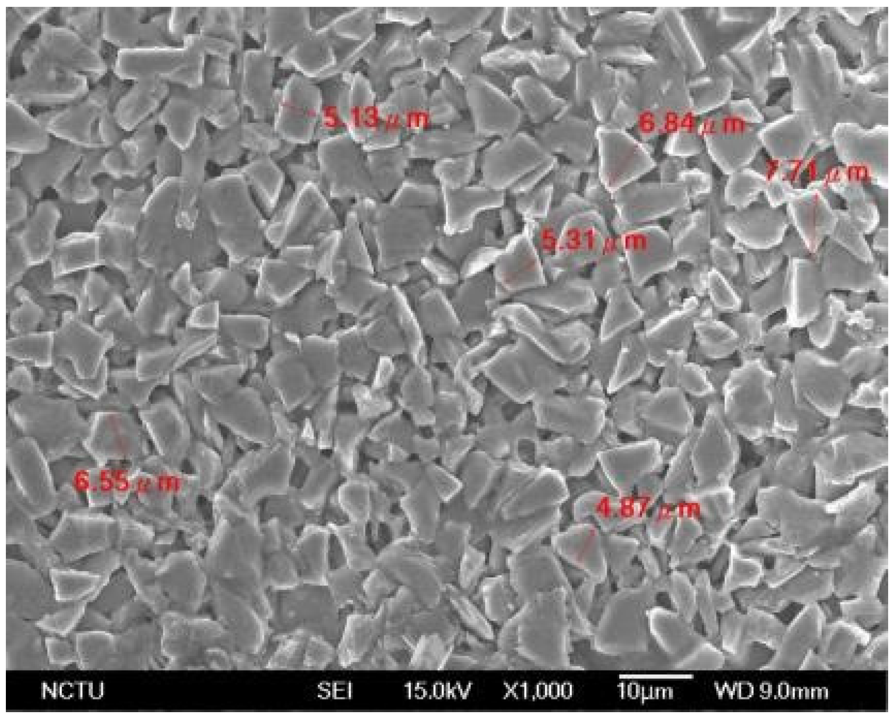
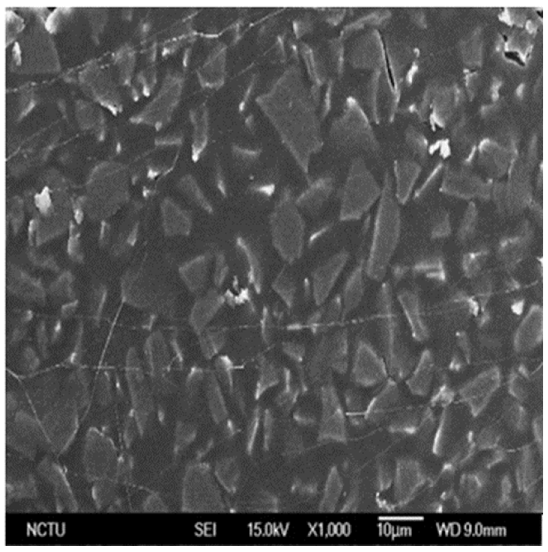
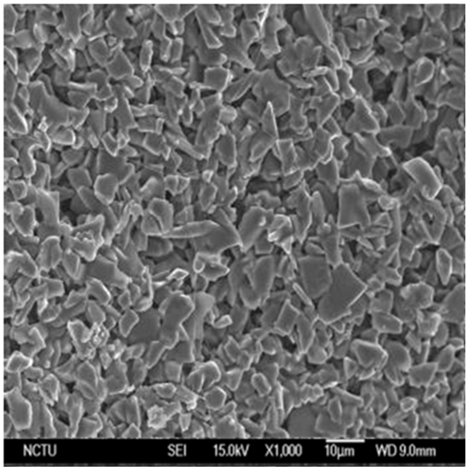
3.1. Scanning Electron Microscopic Microstructural Analysis

A SEM microstructural analysis was performed on absorbent powders of a wave-absorbing composite after blending and on SiC and carbon nanotubes. As shown in Figure 2, the absorbent SiC powder had a smooth appearance, an irregular polygonal shape, and a particle size distribution of approximately 4–10 μm. As shown in Figure 3, the carbon nanotube had adjusted dielectric properties, with a diameter of approximately 20 nm and a length of approximately 50 μm. During the preparation and design of nanocomposites, nanopowders are prone to agglomeration in the substrate, which reduces the amount of dispersion, whose quality affects the reproducibility of the material manufacturing process [9]. Along with the distribution of the absorbent in the absorber material, Figure 4 shows a SEM image of the surface of an SiC 50% + MWCNT 0.2 wt.% absorber composite with a thickness of 1 mm. As shown in the figure, the carbon nanotube exhibits favorable dispersion without agglomeration, which facilitates the stabilization of its properties during the manufacturing process.
Figure 5 shows a SEM image (1000× magnification) of the fractured cross section of an SiC 50% + MWCNT 0.2 wt.% absorber composite with a thickness of 1 mm. This image shows the carbon nanotube shuttled within the SiC powder and connected with SiC to form a conductive network, thereby changing the dielectric properties of the entire absorber material [10].

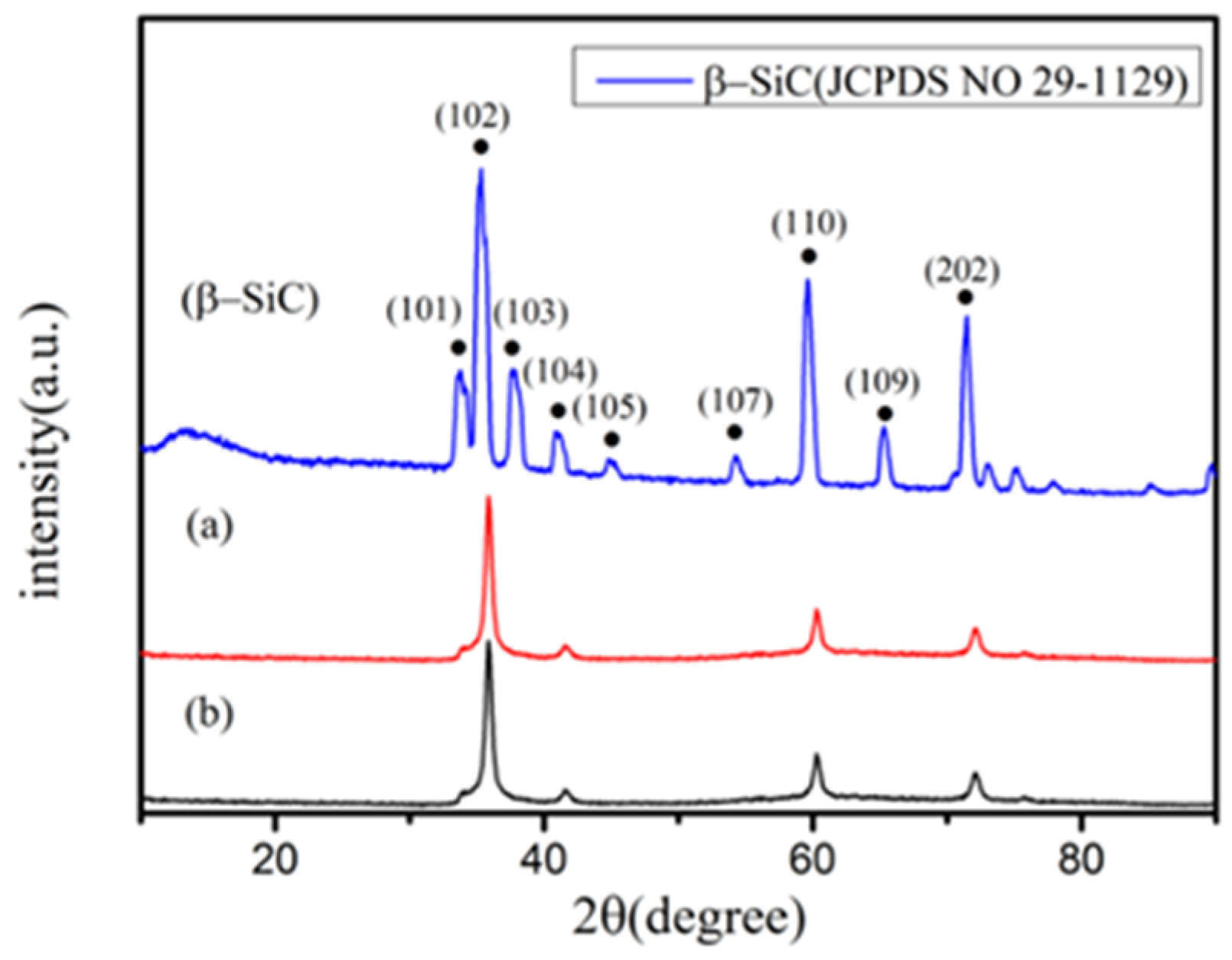
3.2. X-ray Diffraction Structure Determination

Figure 6 shows the XRD analysis of the self-made SiC and SiC 50% + MWCNT 0.1 wt.% mixed powder, in which β-SiC characteristic diffraction peaks appeared separately at 2θ angles of 35.5°, 41.2°, 60°, 72°, and 75.5°. Comparison with the Joint Committee on Powder Diffraction Standards (no. 29-1129) confirmed that the prepared product was a β-SiC component. The peak strength of the SiC powder shown in (a) in Figure 6 was not particularly distinct and contained other impurity phases, presumably because of the peak broadening resulting from the nanocrystallites of SiC. As shown in (b) in Figure 6, after SiC and MWCNTs were mixed, the diffraction peak became weaker because of the considerably reduced carbon nanotube content and presumably became lower than the background value. Therefore, the diffraction peak of the carbon nanotube was not clearly distinguishable.

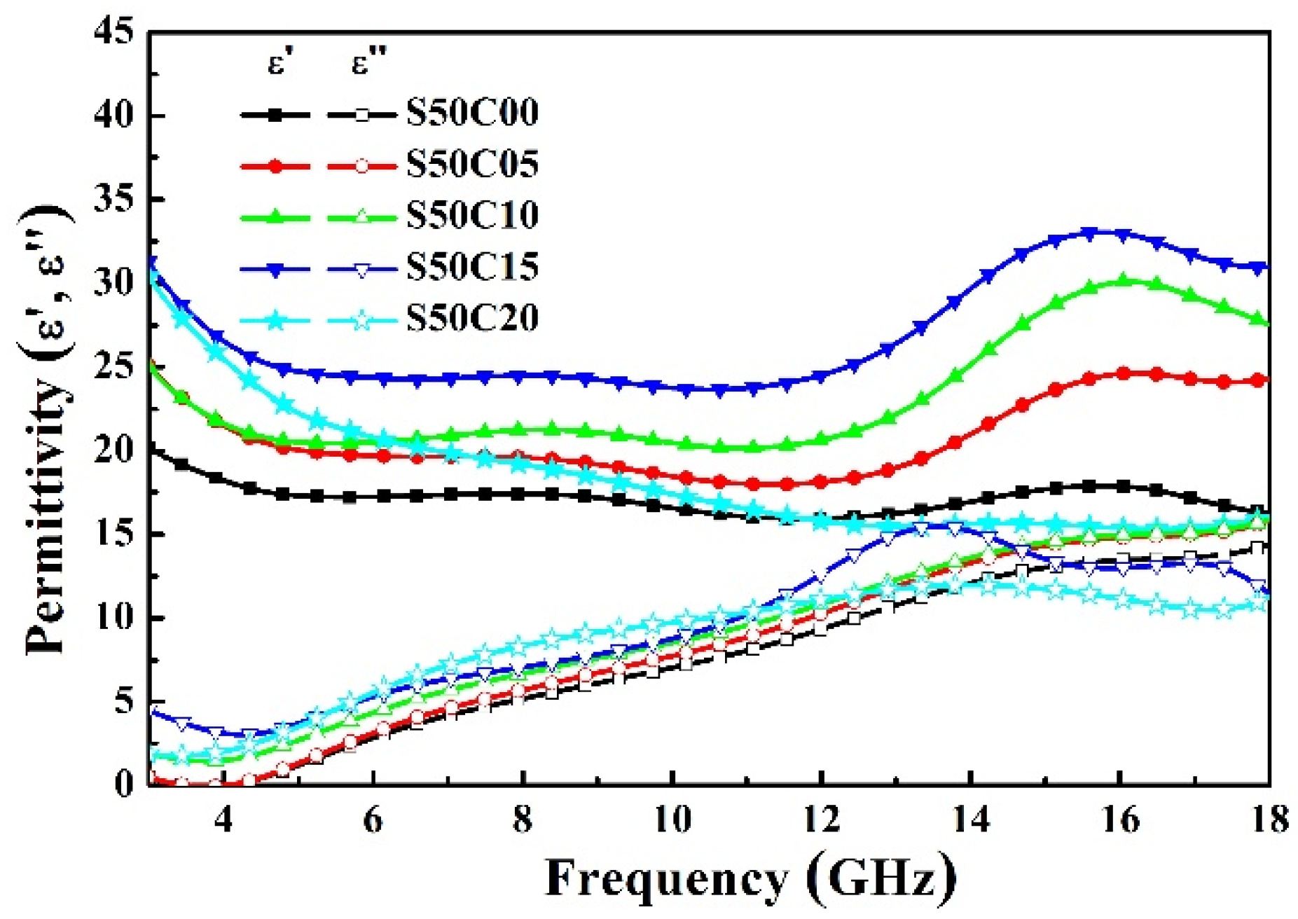
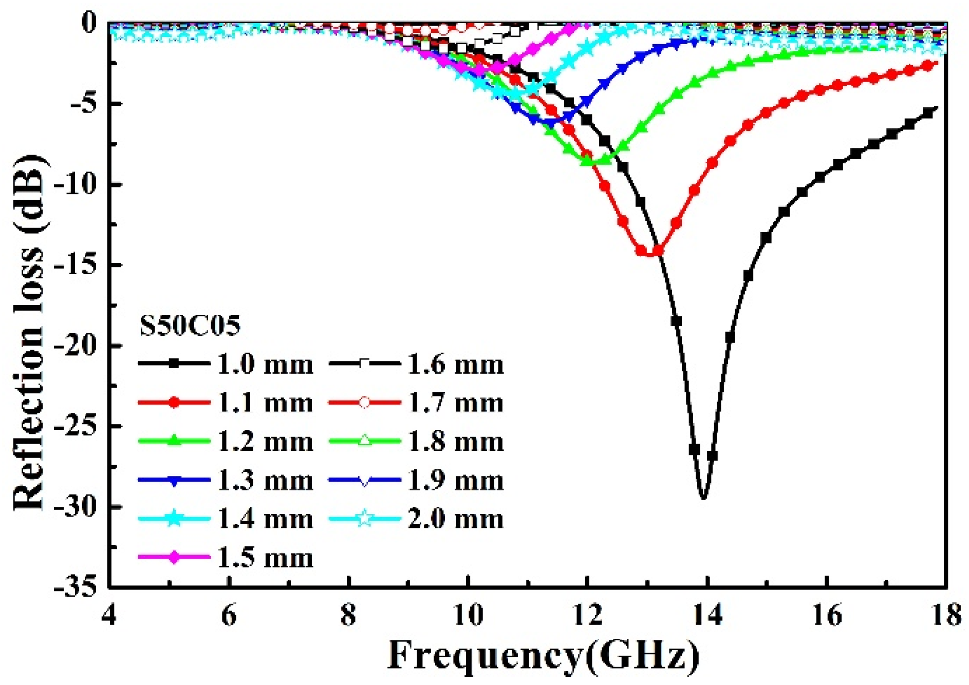
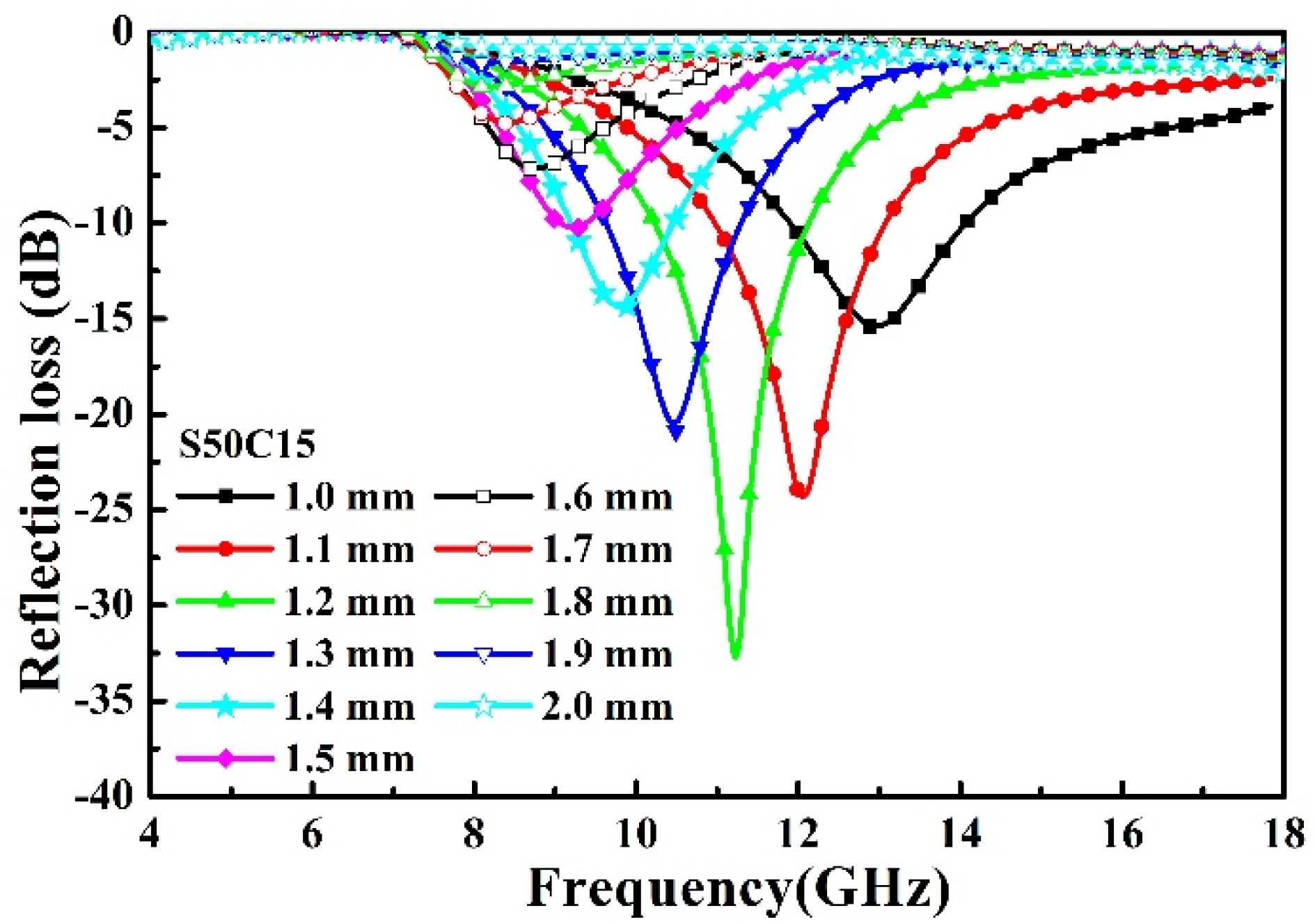
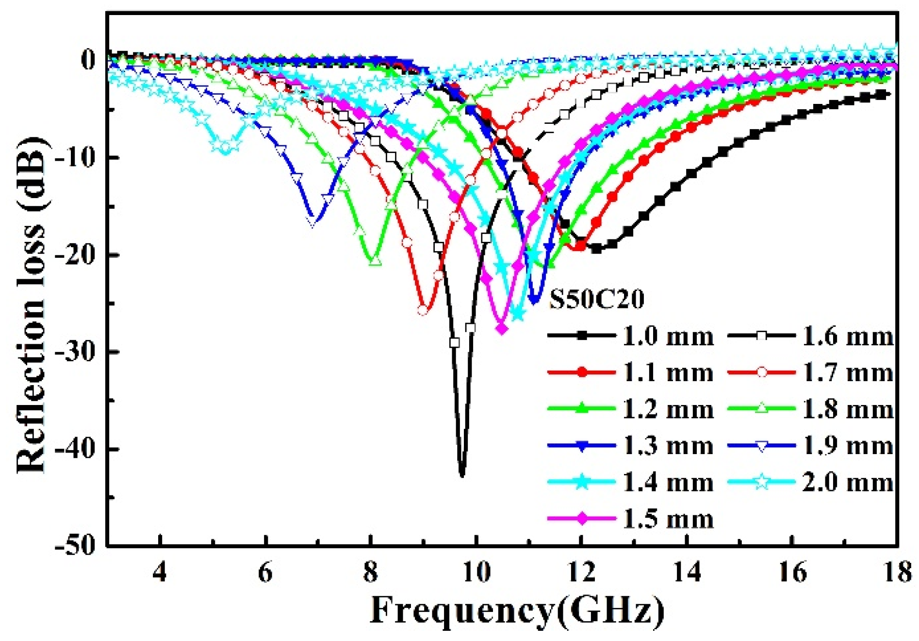
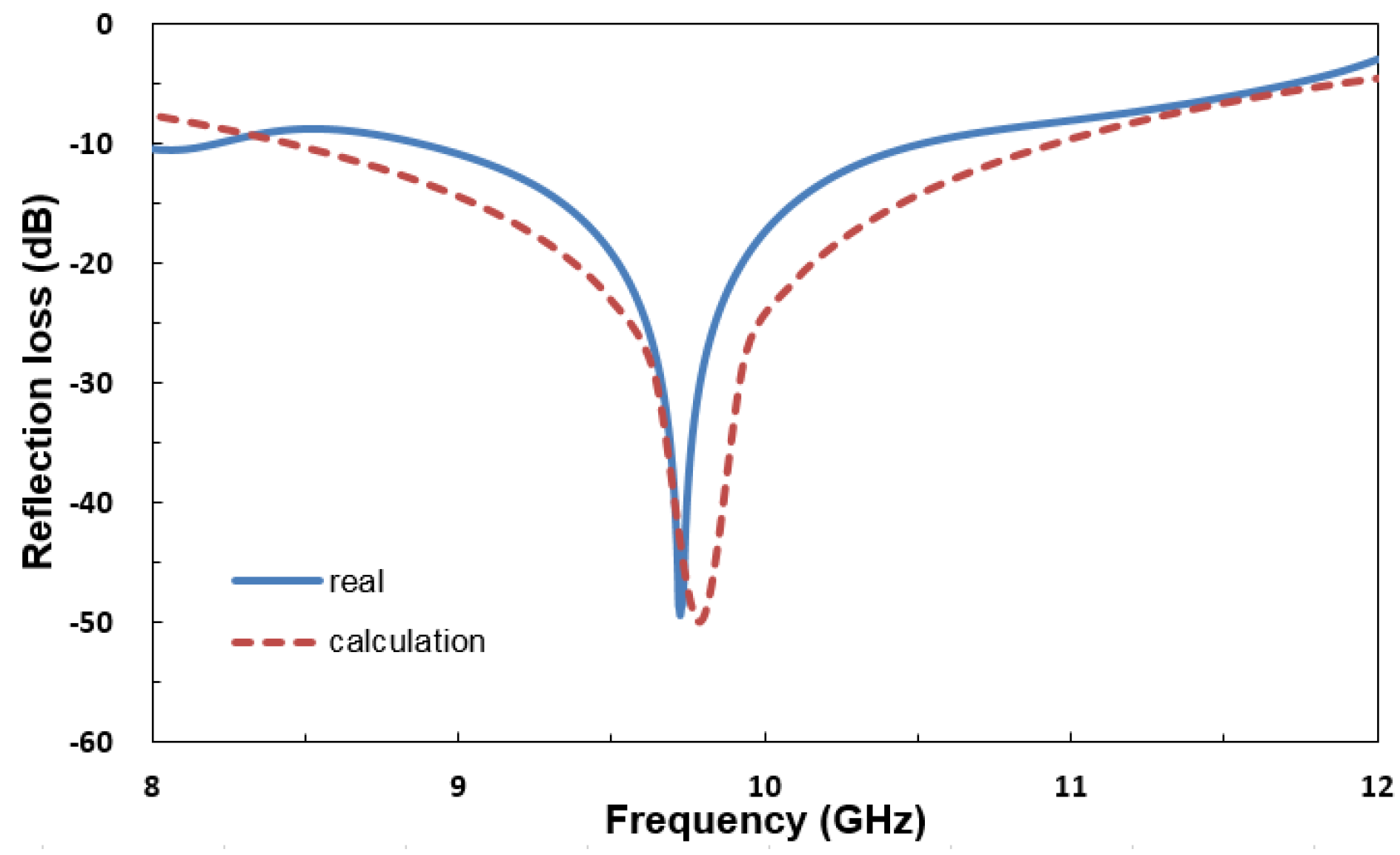
3.3. Microwave Absorption Properties

Absorber strips with a length of 15 cm, a width of 15 cm, and a thickness of 1 mm were produced with different process parameters. In addition, microwave free-space measurement was conducted to assess the electromagnetic parameters (ε′, ε″, μ′, and μ″) of 1 mm thick absorber strips at room temperature. Before measurement, a metal plate of the same size as the test strip was placed for leveling on the measurement location, and the incident angle of the antenna was adjusted to measure the original reflection. A 1 mm thick absorber strip was then placed on a metal plate of the same length and width to measure the electromagnetic wave RL of the strip at 8–12 GHz.
A complex interaction of dielectric and magnetic loss was observed in the electromagnetic wave loss mechanism. The frequency measurement range of complex permittivity and complex permeability was 8–12 GHz. For permittivity, the physical meaning of the real part (ε′) was the magnitude of the dielectric value, whereas the imaginary part (ε″) represented dielectric loss. For permeability, the physical meaning of the real part (μ′) was the permeability size, whereas the imaginary part (μ″) was the magnetic loss.
Figure 7 shows the permittivity values of absorber strips with different amounts of MWCNTs added. At 8–12 GHz, the level of permittivity substantially increased with the increase in the amount of MWCNTs in the test strips. However, when the added amount of MWCNTs exceeded 0.15 wt.%, the permittivity of some frequency bands exhibited attenuation. Generally, because free electrons polarize on different interfaces, permittivity increases because of the accumulation of partial charges on the interface. In addition, MWCNTs have a large specific surface area and dangling bonds, which cause multipoint scattering of electromagnetic waves and increase eddy currents. The presence of MWCNTs dispersed in a composite material is similar to an electron-conducting network, which improves the conducting medium during the accumulation of interface charges, promotes free electron transfer, increases the electrical loss ability, and strengthens the electromagnetic wave attenuation [11,12]. Nonetheless, the presence of excessive MWCNTs does not increase permittivity and rather decreases it, which is related to the reduction of skin depth with the increase in the overall electrical conductivity of the composite material [12].
Figure 8 shows the permeability of the absorber material. Because SiC and MWCNTs are electrical loss absorbents, they do not exhibit a hysteresis effect, and their magnetic loss ability is not substantially affected; thus, all the real parts of permeability approach 1, whereas the imaginary parts approach 0.

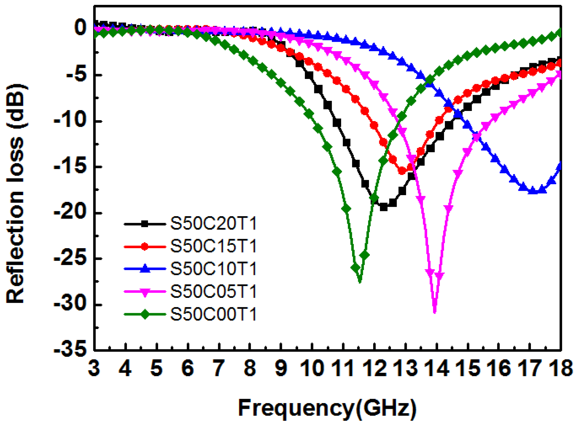
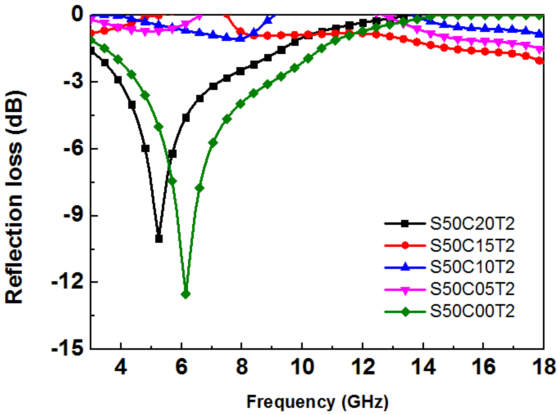
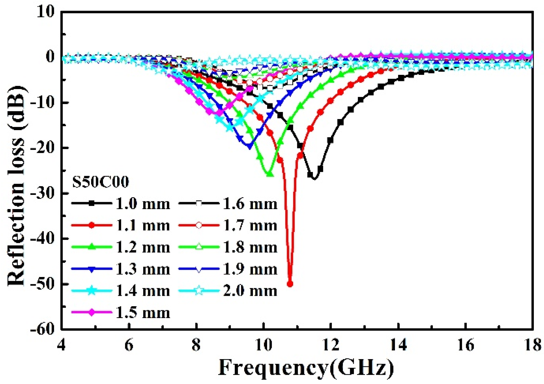
3.4. Reflection Loss Analysis

Figure 9 shows the RL of absorber strips S50C00T1, S50C05T1, S50C10T1, S50C15T1, and S50C20T1. As shown in the figure, strip S50C05T1 exhibited an optimal RL of −31.3 dB at 13.94 GHz, with an RL below −10 dB at frequency bands of 12.74–15.74 GHz. When the test strip thickness increased, the absorption curve tended to shift toward a low frequency. Figure 10 shows the RL of a 2 mm thick test piece. As shown in the figure, only S50C00T2 exhibited a clear RL of −12.5 dB at 6.14 GHz and an optimal RL.
Figure 9 and Figure 10 show the shift in the absorption curves to low frequencies as a result of the increase of the test piece thickness. This phenomenon can be investigated using the formula fm = c/2πμ″d [10], where fm, c, and d represent the matching frequency, speed of light, and sample thickness, respectively. The frequency of minimum reflectance (fm) and its matching sample thickness (dm) can be obtained using dm = c/(4fm μ ε ) [6]. When electromagnetic waves reach the absorber material, multiple scattering occurs between the SiC and MWCNTs in the material. If the specific surface area of the absorbent increases, both polarization and electron holes become more likely to occur at the interface, indicating favorable absorption. Additionally, the return loss of an electromagnetic wave is derived from the destructive interference resulting from its own thickness and the effect of the dielectric loss of the absorber itself in the material.
Because most radars operate in the X-band, their frequency range is 8–12 GHz. According to Maeda et al. [13], optimal radar wave absorption performance can be obtained at RL < −10 dB frequencies. However, in the present study, no favorable absorption occurred (below −10 dB) in the X-band (8–12 GHz) at a thickness of 1 or 2 mm. Therefore, theoretical transmission line formulas (Equations (1)–(9)) were inputted into MATLAB software to theoretically calculate the absorption efficacy of absorber materials prepared with different component proportions at thicknesses of 1–2 mm. Figure 11, Figure 12, Figure 13, Figure 14 and Figure 15 show the simulation diagrams of different component ratios and thickness batches. The results of electromagnetic parameter and thickness matching for each component indicated that the optimal absorption peaks of S50C00, S50C15, and S50C20 appeared on the X-band.
A simulation indicated that an optimal absorption performance can be reached in the X-band at an S50C20 thickness of 1.6 mm. The simulated center frequency of 9.77 GHz had an optimal RL of −49.3 dB, which was regarded as optimal simulation data. Figure 16 shows a center frequency of 9.72 GHz obtained from the S50C20T1.6 test strip prepared according to the simulation, with a maximum RL of −48.9 dB. According to the results, the differences in the shape and particle size between the carbon nanotubes and SiC affected the absorbent dispersion, which in turn resulted in an instability in the electromagnetic effect. Figure 17 shows a flexure image of the S50C20T1.6 absorber material, indicating that the composite absorber material prepared in this study exhibited favorable flexibility.
The composite absorber material S50C20T1.6 exhibited favorable flexibility. It had a maximum absorption peak of −48.9 dB at 9.72 GHz and a bandwidth lower than −10 dB reaching a width of 2 GHz, which satisfied the design concept of a light, thin, wide, and practical absorber material.

4. Conclusions

In this study, flexible SiC/MWCNT absorber materials were prepared using spray coating. MWCNT and thickness adjustments were made to improve the absorption characteristics of the composite material. Excellent absorption was successfully reached at 8–12 GHz (X-band), at which a 1.6 mm thick 50 wt.% SiC + 0.2 wt.% MWCNT absorber strip exhibited an optimal absorption peak in the X-band of −48.9 dB at 9.72 GHz, and bandwidths below −10 dB reached a width of 2 GHz. This satisfied the design concept of a light, thin, wide, and practical absorber material. The as-obtained composite should undergo different trials to determine the effects of environment and weather, how cleaning and degradation will affect the camouflage/stealth performance, and its mechanical and physical properties as well. However, these tests and evaluations have not yet been undertaken in this preliminary work. This must be the next study subject in future.

Author Contributions

This is a joint work and the authors were in charge of their expertise and capability: S.-H.H. for experiment, writing and data analysis; J.-J.Y. for validation and revision; H.D. for investigation and methodology; Y.-Y.L. for writing and revision; J.H. and J.-L.T. for manuscript revision. All authors have read and agreed to the published version of the manuscript.

Funding

This work was funded by Guangdong Basic and Applied Basic Research Foundation (No. 2019A1515111159), Characteristic Innovative Projects for Education Department of Guangdong Province 2021 year (No. 2021KTSCX302).

Data Availability Statement

All data generated or analyzed during this study are included in this published article.

Conflicts of Interest

The authors declare no conflict of interest.

References

  1. Kciuk, M.; Kciuk, S.; Turczyn, R. Magnetorheological characterisation of carbonyl iron based suspension. J. Achiev. Mater. Manuf. Eng. 2009, 33, 135–141. [Google Scholar]
  2. Ding, D.H.; Luo, F.; Zhou, W.C.; Shi, Y.M.; Zhou, L. Research status and outlook of high temperature radar absorbing materials. J. Inorg. Mater. 2014, 29, 461–469. [Google Scholar]
  3. Li, Z.M.; Hu, H.L.; Luo, F. Study process of silicon carbide as high temperature microwave absorber. Rare Met. Mater. Eng. 2007, 36, 96–99. [Google Scholar]
  4. Hu, C.X. Stealth Coating Technology; Chemical Industry Press Co., Ltd.: Beijing, China, 2004; pp. 192–193. [Google Scholar]
  5. Su, X.; Zhou, W.; Xu, J.; Wang, J. Preparation and dielectric property of Al and N Co-doped SiC powder by combustion synthesis. J. Am. Ceram. Soc. 2011, 95, 1388–1393. [Google Scholar] [CrossRef]
  6. Su, X.; Zhou, W.; Xu, J.; Wang, J. Preparation and dielectric property of B and N-codoped SiC powder by combustion synthesis. J. Alloy. Compd. 2013, 551, 343–347. [Google Scholar] [CrossRef]
  7. Ke, Y.C. Polymer-Inorganic Nanocomposites; Chemical Industry Press Co., Ltd.: Beijing, China, 2017; pp. 6–35. [Google Scholar]
  8. Zhang, Y.L.; Li, P.; Shi, L. Stealth Materials; Chemical Industry Press Co., Ltd.: Beijing, China, 2018; pp. 2–10. [Google Scholar]
  9. Xie, S.G.; Jin, Q.; Meng, S.; Wang, Y.W.; Qin, Y.; Guo, X.Y. Microwave absorption properties of in situ grown CNTs/SiC composites. J. Alloy. Compd. 2012, 520, 295–300. [Google Scholar] [CrossRef]
  10. Cao, Y.Z.; Zhang, J.J.; Liang, Y.C.; Yu, F.L.; Sun, T. Mechanical and tribological properties of Ni/Al multilayers-A molecular dynamics study. Appl. Surf. Sci. 2010, 257, 847–851. [Google Scholar] [CrossRef]
  11. Liu, L.D.; Duan, Y.P.; Ma, L.X.; Liu, S.H.; Yu, Z. Microwave absorption properties of a wave-absorbing coating employing carbonyl-iron powder and carbon black. Appl. Surf. Sci. 2010, 257, 842–846. [Google Scholar] [CrossRef]
  12. Bowler, N. Designing dielectric loss at microwave frequencies using muti-layered filler particles in a composite. IEEE Trans. Dielectr. Electr. Insul. 2006, 13, 703–711. [Google Scholar] [CrossRef]
  13. Maeda, T.; Sugimoto, S.; Kagotani, T.; Tezuka, N.; Inomata, K. Effect of the soft/hard exchange interaction on natural resonance frequency and electromagnetic wave absorption of the rare earth–iron–boron compounds. J. Magn. Magn. Mater. 2004, 281, 195–205. [Google Scholar] [CrossRef]
Figure 1. Free-space measurement.
Symmetry 14 02144 g001
Figure 2. SEM image of SiC powder.
Symmetry 14 02144 g002
Figure 3. SEM image of a carbon nanotube.
Symmetry 14 02144 g003
Figure 4. SEM image of the absorber composite surface.
Symmetry 14 02144 g004
Figure 5. SEM image of the fractured cross section of the absorber composite.
Symmetry 14 02144 g005
Figure 6. XRD image: (a) self-made SiC, (b) mixed powder.
Symmetry 14 02144 g006
Figure 7. Permittivity values of 50 wt.% SiC with different amounts of MWCNTs added.
Symmetry 14 02144 g007
Figure 8. Real and imaginary part values for the permeability of 50 wt.% SiC with MWCNT absorber strips added.
Symmetry 14 02144 g008
Figure 9. RL of 1 mm thick 50 wt.% SiC with MWCNTs added.
Symmetry 14 02144 g009
Figure 10. RL of 2 mm thick 50 wt.% SiC with MWCNTs added.
Symmetry 14 02144 g010
Figure 11. Thickness and RL simulation for S50C00.
Symmetry 14 02144 g011
Figure 12. Thickness and RL simulation for S50C05.
Symmetry 14 02144 g012
Figure 13. Thickness and RL simulation for S50C10.
Symmetry 14 02144 g013
Figure 14. Thickness and RL simulation for S50C15.
Symmetry 14 02144 g014
Figure 15. Thickness and RL simulation for S50C20.
Symmetry 14 02144 g015
Figure 16. Comparison between measured and simulated values for S50C20T1.6.
Symmetry 14 02144 g016
Figure 17. Flexure of S50C20T1.6.
Symmetry 14 02144 g017
Table 1. Experiment planning for a microwave-absorbing test strip.
GroupSiC Weight Ratio %MWCNT Added Ratio wt%Thickness (mm)
S50C00T150:500.001
S50C00T20.002
S50C05T10.051
S50C05T20.052
S50C10T10.101
S50C10T20.102
S50C15T10.151
S50C15T20.152
S50C20T10.201
S50C20T20.202
Publisher’s Note: MDPI stays neutral with regard to jurisdictional claims in published maps and institutional affiliations.

