Abstract
In today’s TEST interconnected world, the security of 5G Medical IoT networks is of paramount concern. The increasing number of connected devices and the transmission of vast amounts of data necessitate robust measures to protect information integrity and confidentiality. However, securing Medical IoT edge nodes poses unique challenges due to their limited resources, making the implementation of cryptographic protocols a complex task. Within these protocols, modular multiplication assumes a crucial role. Therefore, careful consideration must be given to its implementation. This study focuses on developing a resource-efficient hardware implementation of the Montgomery modular multiplication algorithm over GF(), which is a critical operation in cryptographic algorithms. The proposed solution introduces a bit-serial systolic array layout with a modular structure and local connectivity between processing elements. This design, inspired by the principles of symmetry, allows for efficient utilization of resources and optimization of area and delay management. This makes it well-suited for deployment in compact Medical IoT edge nodes with limited resources. The suggested bit-serial processor structure was evaluated through ASIC implementation, which demonstrated substantial improvements over competing designs. The results showcase an average area reduction of 24.5% and significant savings in the area–time product of 26.2%.
Keywords:
bit-serial systolic array; cryptographic protocols; edge computing; Medical IoT; Montgomery modular multiplication MSC:
11T71
1. Introduction
The field of the Medical Internet of Things (MIoT) has experienced significant growth with the widespread adoption of IoT technologies. This growth has brought about a revolution in healthcare by enabling the seamless integration of connected devices, data collection, and cloud-based analysis, allowing for informed decision-making. The potential of MIoT in healthcare is further amplified by the emergence of 5G MIoT networks, which leverage the capabilities of 5G technology to provide high-speed, low-latency, and reliable connectivity for various medical applications, including remote patient monitoring, telemedicine, and real-time data analytics [1,2,3,4].
A typical remote patient monitoring system consists of various medical IoT devices deployed in patients’ homes, including wearable sensors, implantable devices, and home-based gateways. These devices continuously collect data on vital signs, such as heart rate, blood pressure, glucose levels, and activity levels, from patients. The collected data are then transmitted over a 5G network to a central healthcare facility, where clinicians can remotely monitor patients’ health and make informed decisions about their care. However, Medical IoT devices at the edge of the network often have significant resource constraints. These edge devices are typically battery-powered and have limited processing power, memory, and energy resources, making it challenging to implement complex security and data processing algorithms. Addressing the security and performance needs of these resource-constrained medical IoT devices is a critical challenge in ensuring the confidentiality, integrity, and availability of sensitive patient data in remote monitoring applications [5].
One potential solution to this challenge is the implementation of optimized cryptographic algorithms on these constrained MIoT nodes [6,7,8]. These algorithms are specifically designed to operate efficiently within the limitations of the devices, allowing edge nodes to perform essential security operations without overwhelming their limited resources and computational capabilities. This approach strikes a balance between security and resource utilization, enabling edge nodes to effectively protect medical data within their constraints.
Among the various available cryptographic techniques, one that has garnered particular attention for deployment on resource-constrained MIoT edge nodes is Elliptic Curve Cryptography (ECC). ECC offers optimized cryptographic algorithms specifically tailored to operate efficiently within the limitations of devices with limited resources. Central to these algorithms are finite-field arithmetic operations, with finite-field multiplication serving as a fundamental operation that significantly impacts the efficiency and performance of related field operations such as inversion, division, and exponentiation.
There is a growing emphasis on promoting the use of compact yet highly effective cryptographic algorithms that rely on efficient finite-field multiplication. These algorithms aim to strike a delicate balance between the demanding security requirements and the resource constraints inherent in MIoT edge nodes. By optimizing finite-field multiplication and related operations, these algorithms enable the implementation of secure and efficient cryptographic protocols within the limited computational capabilities of MIoT devices.
2. Related Work
Researchers have explored different approaches and techniques to optimize the multiplication operation over GF() [9,10,11]. Numerous studies have focused on reducing the area and delay complexities of this operation, aiming to enhance the efficiency and performance of computer algebra applications dependent on GF() computations [12,13,14]. These efforts have led to a significant body of literature discussing various methodologies, algorithms, and architectures aimed at minimizing the area and delay overhead of multiplication in GF() [15,16,17,18,19,20,21,22].
A Galois field (GF()) can be represented using different bases, including polynomial basis (PB), normal basis (NB), and dual basis (DB). Among these options, the polynomial basis (PB) is often considered the best choice due to its simplicity and compatibility with typical hardware constructions, eliminating the need for base conversion [23].
Multiplication in GF() is a more complex operation compared to simple addition and subtraction. It involves two distinct steps, namely polynomial multiplication and modulo reduction using an irreducible polynomial. In the context of GF(), several types of irreducible polynomials exist, such as All-One Polynomials (AOPs), Equally Spaced Polynomials (ESPs), trinomials, and pentanomials. These irreducible polynomials serve as essential components in the modulo reduction process, ensuring the integrity and correctness of the multiplication operation in GF().
The literature encompasses various hardware architectures for implementing polynomial basis (PB) multiplication in GF(), including bit-parallel, bit-serial, and digit-serial multipliers. Bit-parallel multipliers, despite their significant space complexity, offer the advantage of performing field multiplication in a fixed number of iterations, irrespective of the field size (l) [24]. This characteristic makes them desirable for certain applications where a predictable and consistent multiplication time is crucial. Bit-parallel multipliers achieve this fixed-iteration property by simultaneously processing multiple bits of the operands in parallel, resulting in efficient and predictable multiplication operations.
The design of systolic architectures has emerged as a prominent research direction in this field. Lee and Yoo [10] proposed a linear systolic multiplier/squarer architecture for fast exponentiation. Fenn et al. [12] developed a dual-basis bit-serial systolic multiplier for GF(). Kim and Jeon [15,16] introduced a polynomial-basis multiplier using a cellular systolic architecture, as well as a semi-systolic Montgomery multiplier over GF(). Choi and Lee [17] designed an efficient systolic modular multiplier/squarer for fast exponentiation over GF(). Ibrahim [19,22] presented novel bit-serial semi-systolic array structures for simultaneously computing field multiplication and squaring, as well as efficient parallel and serial systolic structures for these operations over GF(). Kim and Lee [20] explored efficient, unified semi-systolic arrays for multiplication and squaring over GF(), while Kim [21] proposed an efficient bit-parallel systolic architecture.
Systolic multiplier topologies, based on systolic arrays, leverage the concept of symmetry to enhance performance. These architectures provide a regular and structured design with balanced arrangements and repeated patterns, enabling efficient parallel processing and concurrent data flow. By incorporating symmetry, systolic multipliers achieve optimized resource utilization, streamlined data movement, and increased throughput. However, the introduction of symmetry also introduces trade-offs, such as increased hardware complexity and potential latency due to additional circuitry and delays within the symmetrical arrangement. Therefore, careful consideration is necessary to strike a balance between leveraging symmetry for improved throughput and managing latency concerns in the systolic array design [20,21,22,25,26,27,28].
In cryptography applications with limited resources, bit-parallel architectures may not be the optimal choice due to their high hardware requirements. Instead, bit-serial multiplier designs offer a good trade-off between speed and space, making them well-suited for cryptographic applications with stricter space and power limitations [11,12,16,17,18,19,29,30]. Bit-serial multipliers excel in scenarios where there are constraints on available hardware resources. They enable efficient multiplication with minimal hardware requirements, making them suitable for cryptographic applications with restricted resources. While bit-serial multipliers may require more time to generate the multiplication result compared to bit-parallel architectures, their advantage lies in their ability to achieve a good speed/space trade-off [31,32,33,34,35]. On the other hand, bit-serial multipliers are not as performance-scalable as bit-parallel architectures. They need at least l time steps, where l is the field size, to obtain the overall multiplication product, which may limit their applicability in scenarios where performance is a critical factor.
The main goal of this study is the development of a bit-serial systolic implementation of the field Montgomery multiplication algorithm presented in [36] for effective multiplication operations over GF(). The algorithm utilizes a general irreducible polynomial as its foundation and offers advantages such as reduced latency and minimized time and area overhead by using the same architecture for iterative parts of the algorithm. The implementation process involves utilizing the derived dependency graph (DG) of the multiplication method and investigating the bit-serial multiplier construction through the selection of appropriate scheduling and projection vectors. The bit-serial systolic array structure was generated by mapping the DG nodes to the relevant processing elements (PEs) and assigning the appropriate time to the DG nodes using the chosen scheduling and projection vectors. This construction allows for efficient and optimized multiplication operations.
The developed bit-serial multiplier harnesses the concept of symmetry to achieve perfect resource utilization and a reasonable multiplication speed. This is accomplished by leveraging the benefits of the bit-serial systolic array structure, which exhibits symmetrical properties in its balanced arrangements and recurring patterns. Additionally, careful setting of the scheduling and projection vectors further enhances the utilization of resources and optimizes the data flow within the systolic array. As a result, this work contributes to the development of compact cryptographic processors by presenting a novel method for implementing the Montgomery Modular multiplication algorithm over GF() with reduced hardware complexity and increased space efficiency. By incorporating symmetry, the proposed approach demonstrates its suitability for use in compact MIoT nodes, where limited resources necessitate efficient designs.
The constructed bit-serial systolic multiplier arrangement was thoroughly evaluated using ASIC technology, and the reported results reveal the overall benefits of the proposed design. Notably, the presented solution outperforms the competing approaches, achieving significantly higher area efficiency and beating them by at least 24.5%. Moreover, when evaluating the designs using the combined area–time (AT) metric, the proposed architecture outperforms the competing solutions by a margin of at least 26.2%. Crucially, the significant improvements in area efficiency, combined with the competitive AT results, firmly establish the proposed bit-serial systolic multiplier structure as the preferred option over the existing alternatives. This comprehensive analysis highlights the substantive advantages of the new solution, making it a compelling choice for further development and implementation.
This paper follows a structured organization, starting with Section 3, which provides a concise explanation of the adopted Montgomery multiplication algorithm for . Moving on to Section 4, the focus shifts to the examination of the explored DG of the adopted algorithm. Attention switches to the bit-serial systolic array multiplier structure in Section 5, diving into its design and implementation aspects. Section 6 then assesses the area and time complexities of both the recommended multiplier layout and the observed effective bit-serial architectures. Finally, in Section 7, the paper concludes by summarizing the main findings and highlighting potential future research directions.
3. Montgomery Modular Multiplication over GF()
Let us define the irreducible polynomial that generates the finite field GF() as follows:
The polynomial F represents the sum of terms, where each term has a coefficient () and the variable raised to the power of j. In this polynomial expression, coefficients and are assumed to be equal to one.
In GF(), each element is represented as a unique linear combination of polynomials with degrees less than l. The addition of two polynomials in GF() is straightforward and can be achieved using bitwise exclusive-OR (XOR). However, multiplication of two polynomials in GF() is more complex, as it involves an intermediate result that requires additional modular reduction by .
Let us consider a scenario with two elements in GF(), namely and ; the task is to perform Montgomery Modular Multiplication (MMM). Montgomery residues C and D are given, which are the modular reductions of and , respectively. Additionally, a special element (Q) is provided that satisfies the condition of .
The MMM computation of and involves the following steps:
- Compute , where represents the modular inverse of Q with respect to F;
- Obtain the final result (K) by performing Montgomery multiplication using inputs P and 1, i.e., .
Montgomery multiplication offers significant advantages for applications that involve repeated multiplications, such as inversion, exponentiation, and elliptic curve point multiplication. The use of Montgomery multiplication is particularly beneficial in these scenarios due to the specific criteria for pre- and post-transformation [37].
The Montgomery equation, , can be described more succinctly using the special element of , as follows [36]:
Equation (2) can be rewritten in the following manner:
It is important to note that odd values of l are frequently employed in real applications. As a result, using odd l values will be the main consideration when creating the multiplier.
To obtain the recursive variants of Equations (4) and (5), they must be reordered in the following manner:
Let and denote the results of the iteration of Equations (6) and (7), respectively. These values are calculated iteratively based on the previous pair of iterators’ results. The iterative form for Equation (6) at step i, , can be stated as follows, capturing the iterative aspect of the calculation.
where .
It is worth noting that calculating the end result of requires the necessary condition of . Furthermore, since there is no data dependency between and , they can be computed concurrently, as depicted by Equations (8) and (9).
To obtain the reduced form of , , in the bit-level representation, the expansion of in Equation (8) can be substituted. By doing so, the following bit-level expression for is obtained:
The following is a representation of the iterative form of A at step i:
where and .
Using the assumption that is a root of irreducible polynomial F and that , the formula can be obtained by multiplying both sides of F by . This allows for a simple representation of the inverse of in terms of its powers.
can be rewritten in exactly the same way as demonstrated in Equation (10) by substituting the expanded value of into Equation (9).
The following is a representation of the iterative form of B at step i:
where for .
To obtain the final result (P), the addition of and can be accomplished by employing a total of l two-input XOR gates.
The algorithmic structure for the formulas described earlier can be represented by two algorithms, namely Algorithms 1 and 2. Algorithm 1 represents the high-level version, while Algorithm 2 is a bit-level variant.
| Algorithm 1 Montgomery Modular Multiplication Method over GF(). |
| Input: , and F |
| Output: P |
| Initialization: |
| Algorithm: |
|
| Algorithm 2 Bit-level version of the Montgomery Modular Multiplication Algorithm. |
| Input: |
| Output: |
| Initialization: |
| Algorithm: |
|
4. Dependency Graph
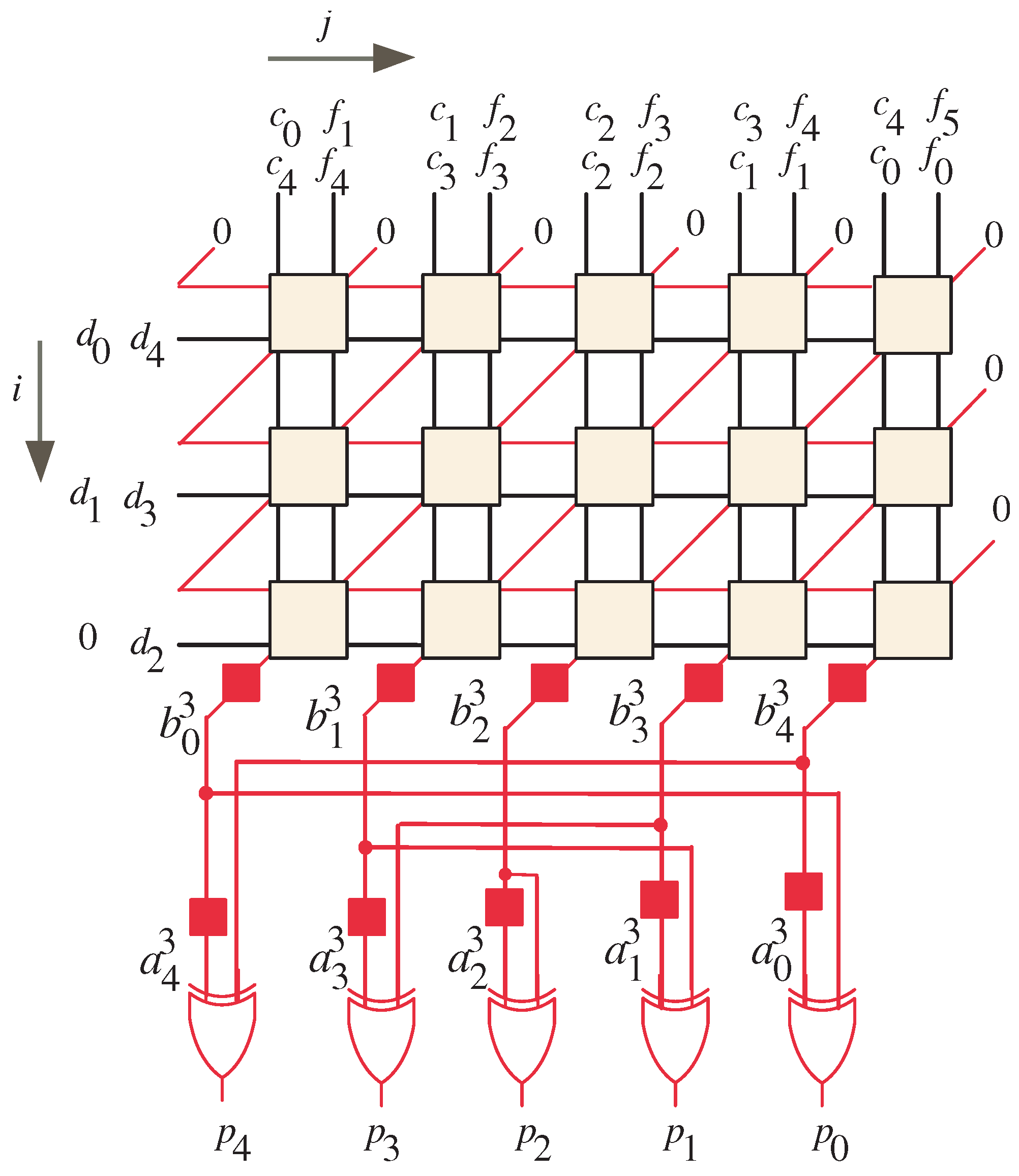
The iterative portion of the Montgomery multiplication algorithm involves a series of computations that can be described by two recursive equations, namely Equation (11) and Equation (13). These equations share a common characteristic, namely that they possess a similar and independent computational structure. This similarity allows the computations to be represented using a unified dependency graph (DG), which captures the interdependencies among them. Examining Figure 1, which illustrates the extracted dependency graph for a specific value of l (in this case, ), can provide insights into the computational relationships within the algorithm.
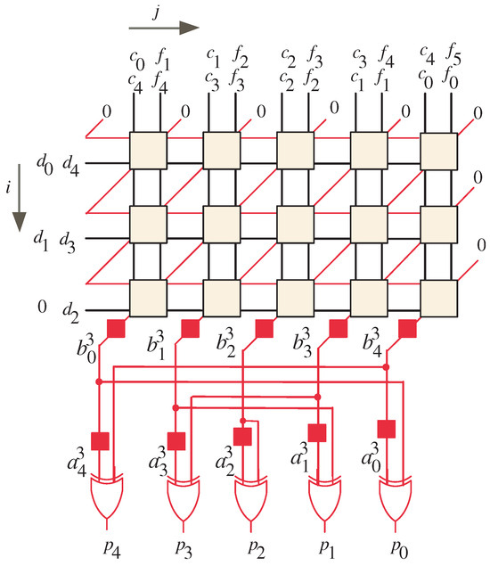
Figure 1.
DG of the Montgomery algorithm for the case when .
The DG is represented within a two-dimensional integer domain () defined by the indices i and j. Within this domain, the DG consists of nodes that correspond to the operations described by Equations (11) and (13). These nodes are responsible for performing the necessary calculations during the iterative process. Notably, the coefficients of A and B are computed sequentially, with the computation of A preceding that of B. To streamline the computation of the coefficients of B, the coefficients of C, D, and F are carefully arranged in a manner that allows for the reuse of the same processing node. This optimization helps to reduce computational redundancy and enhance the efficiency of the algorithm.
The initial placements of the input signals in the dependency graph (DG) follow a specific pattern. Let us examine the arrangement in detail.
- Input signals and , where , are sequentially entered into the DG nodes from the left side;
- Input signals and are also entered sequentially into the DG nodes but, this time, from the top of the graph;
- Similarly, input signals and are entered sequentially from the top of the DG.
To initialize the computation, input signals and are set to a value of 0. These signals are indicated by slanted red lines and are entered sequentially into the right corners of the corresponding input nodes. As the computation progresses, each node performs its calculations and passes the resulting signals to the nodes in the next row. This process allows for the computation of intermediate partial products.
The final result, denoted as P, is obtained by summing the coefficients of and . It is worth noting that there is a one-clock cycle delay between and . This delay is achieved by employing two latches, which are denoted by the red boxes at the bottom of the DG. To perform the summation, two-input XOR gates are utilized. These gates combine the corresponding coefficients of and to generate the final result, P.
5. Development of the Bit-Serial Systolic Array
To construct the bit-serial systolic array, it is crucial to select suitable scheduling and projection vectors for application to the dependency graphs (DGs). In accordance with the methodology described in [22,38,39,40], we can select the scheduling vector denoted as and the projection vector denoted as to facilitate the design of the bit-serial systolic structure. For this specific case, the scheduling vector is chosen as , while the projection vector is .
By applying the selected scheduling and projection vectors to the nodes () within the DGs, the scheduling function () and the projection function () can be established as follows:
The scheduling function assigns each DG node a specific time value, which determines when the computation at that particular node should occur within the systolic array. On the other hand, the projection function maps each DG node to its designated processing element (PE) within the systolic array, ensuring that the computation is performed at the intended location within the architecture.
By employing the concept of symmetry through the scheduling and projection functions derived from the scheduling vector () and the projection vector (), the DG (Data Generation) nodes can be effectively scheduled and projected onto the associated processing elements (PEs) within the bit-serial systolic array. This systematic approach, based on symmetrical properties, ensures balanced distribution of computational tasks and streamlined data movement, thus facilitating the efficient execution of computations within the systolic architecture. As a result, this approach optimizes performance and resource utilization, leveraging the inherent benefits of symmetry in the design of the bit-serial systolic array.
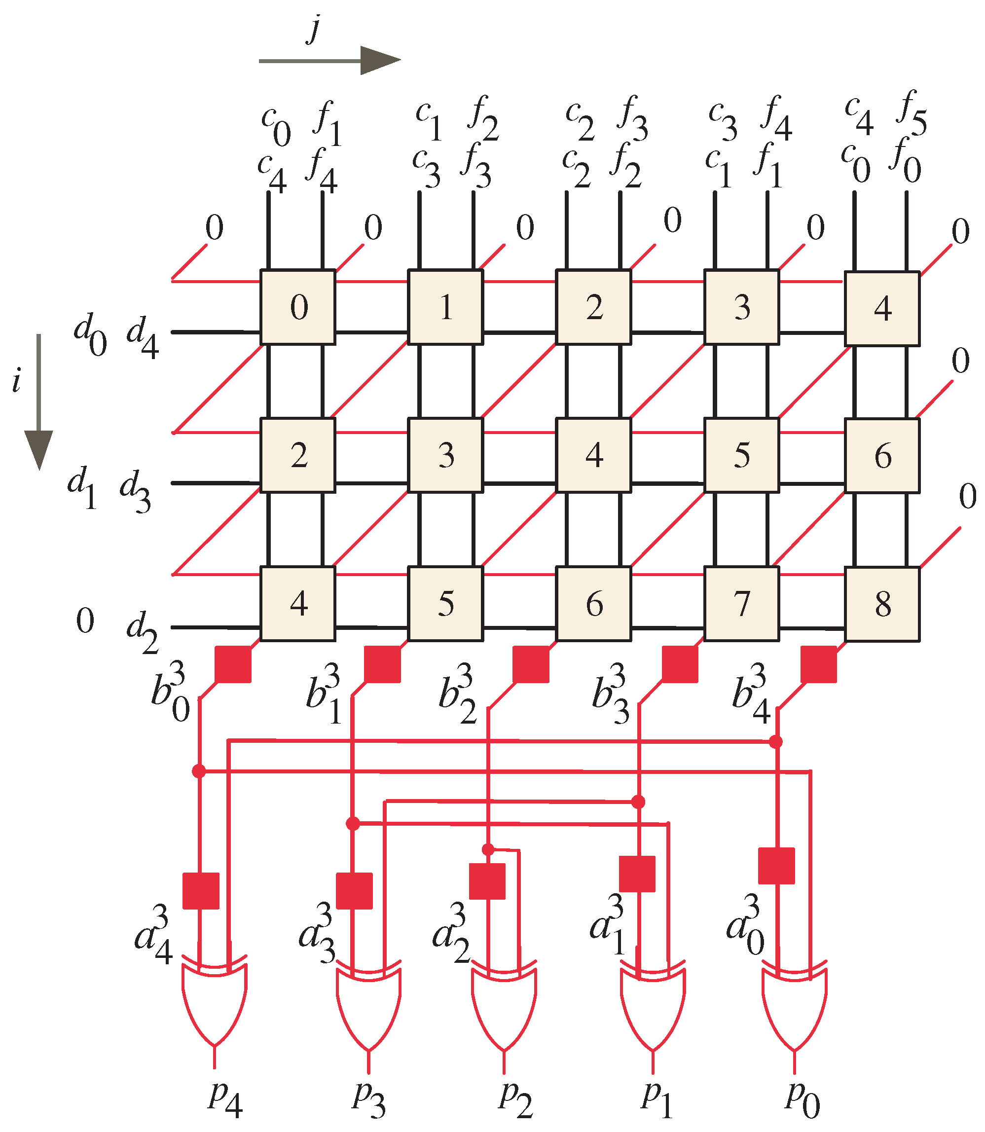
The resulting node timing after applying the scheduling function () to the dependency graph (DG) can be observed in Figure 2. By examining Figure 2, it is evident that the timing values assigned to the nodes follow a progressive pattern. The inputs are applied successively, and the computations within the DG progress accordingly, generating the intermediate products in a sequential manner. Overall, the scheduling function () aids in orchestrating the timing of computations within the DG, ensuring the proper flow and synchronization of operations in the bit-serial systolic array. This enables the efficient utilization of resources and facilitates the accurate generation of intermediate products.
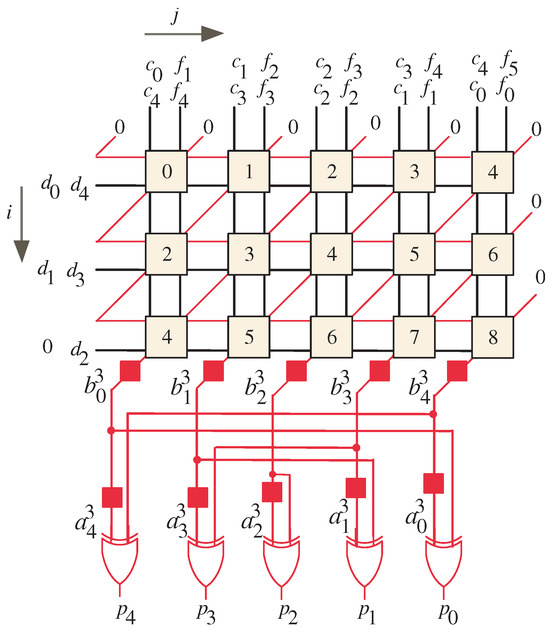
Figure 2.
Node timing for .
According to the given description, the processor array operates in a sequential manner to process the inputs and generate the output results of A and B. A summary of the timing and sequence of operations is presented as follows:
- From time step 0 to time step :
- The input bits (, , , and ) are applied in sequence;
- The resulting output bits of A, , are presented one bit at a time;
- The output bits of A are produced starting with the Most Significant Bit (MSB), , at time and ending with the Least Significant Bit (LSB), , at time .
- From time step l to time step :
- The input bits (, , , and ) are applied in sequence;
- The resulting output bits of B, , are presented one bit at a time;
- The output bits of B are produced starting with the LSB, , at time and ending with the MSB, , at time .
Therefore, the processor array requires a total of time steps to produce the output results of A and B, where l is the number of bits in the input vectors.
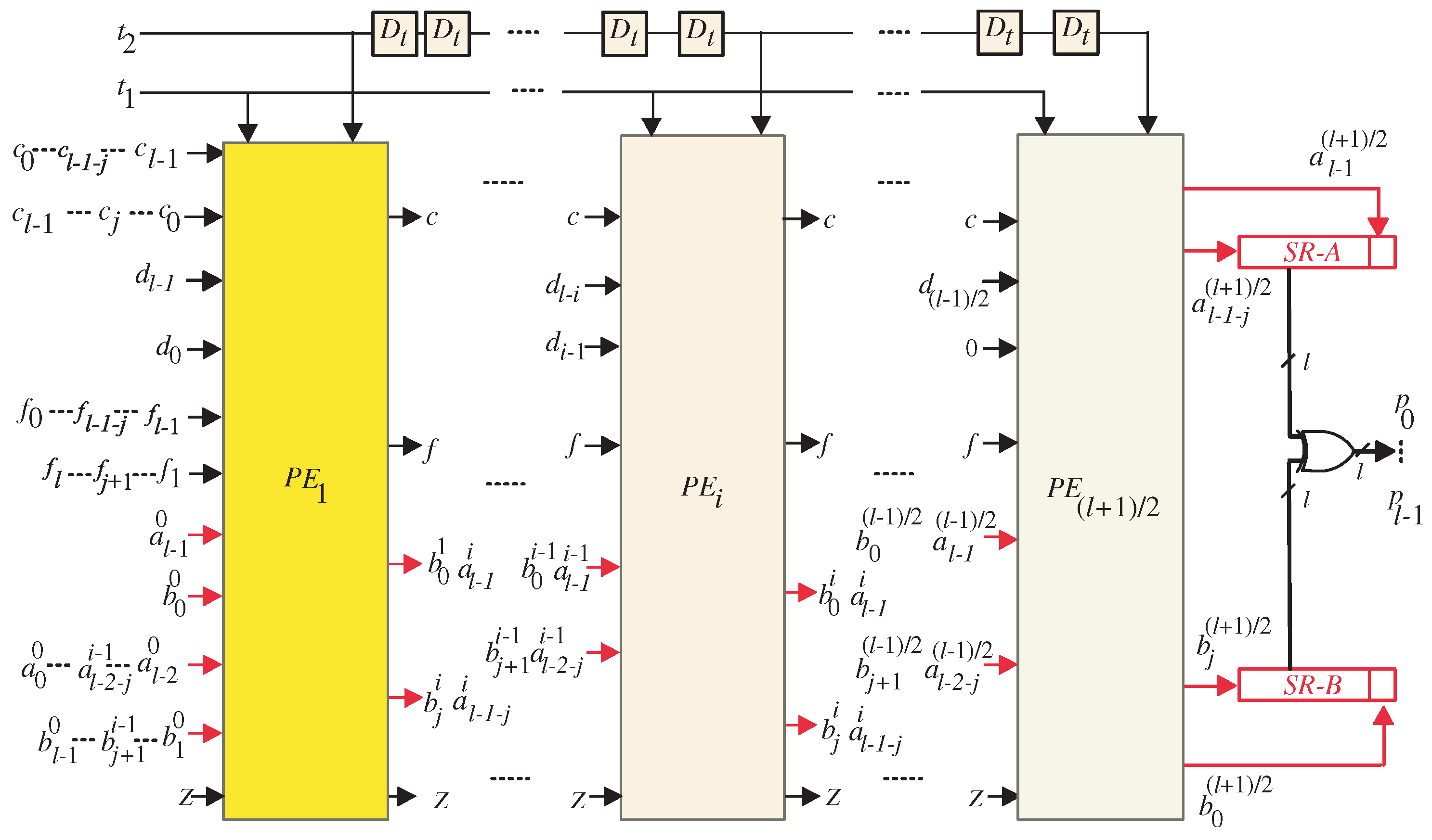
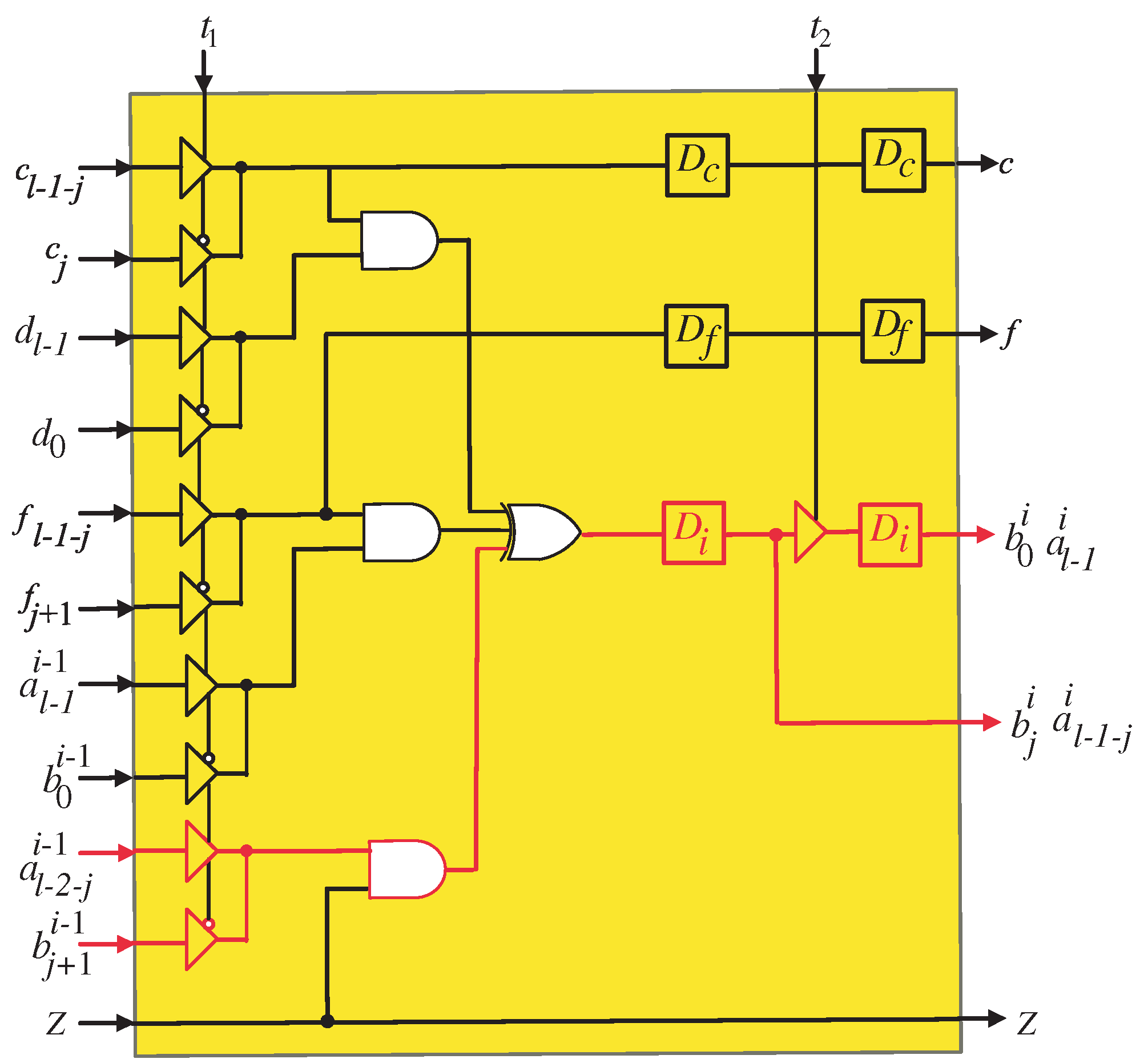
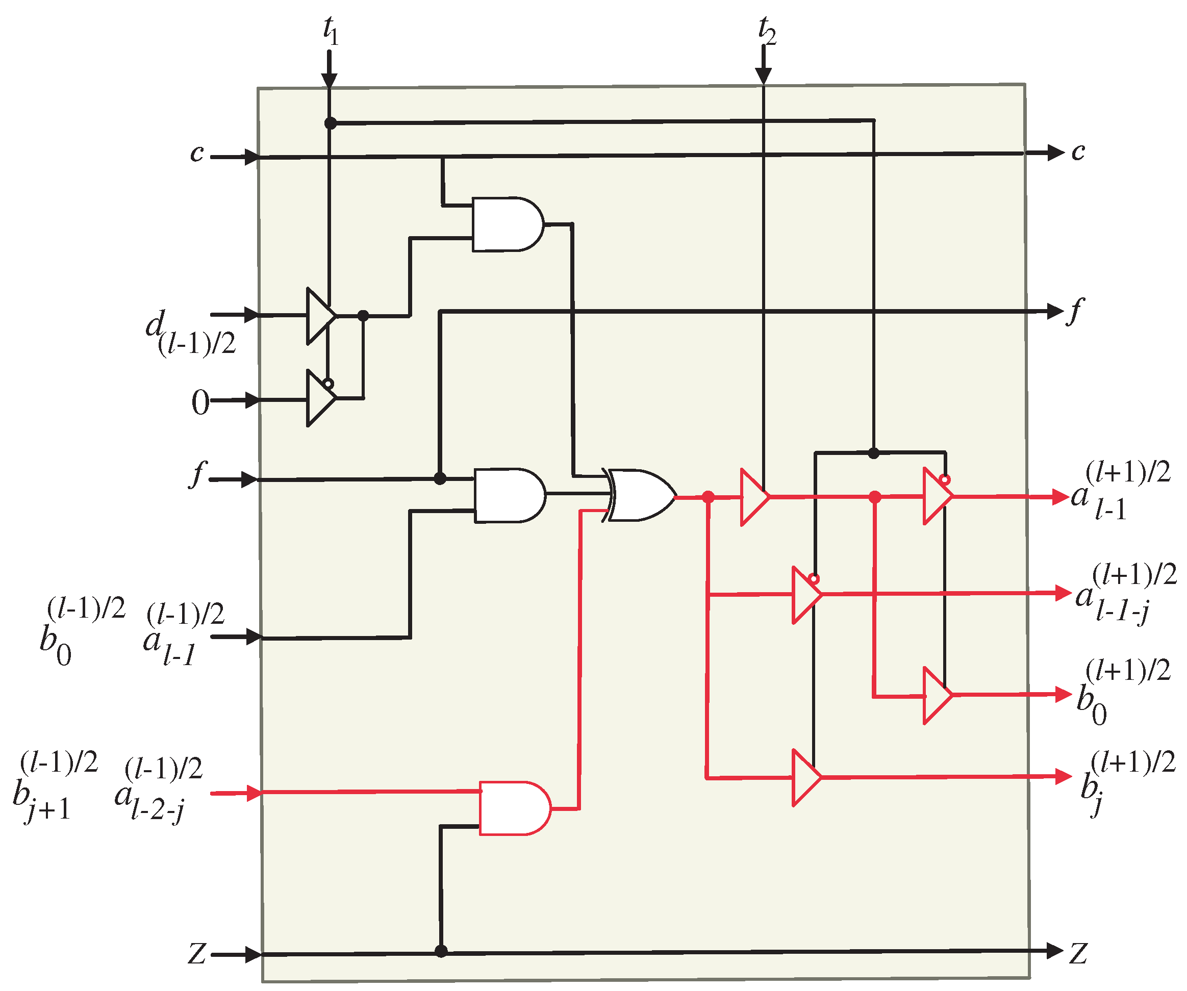
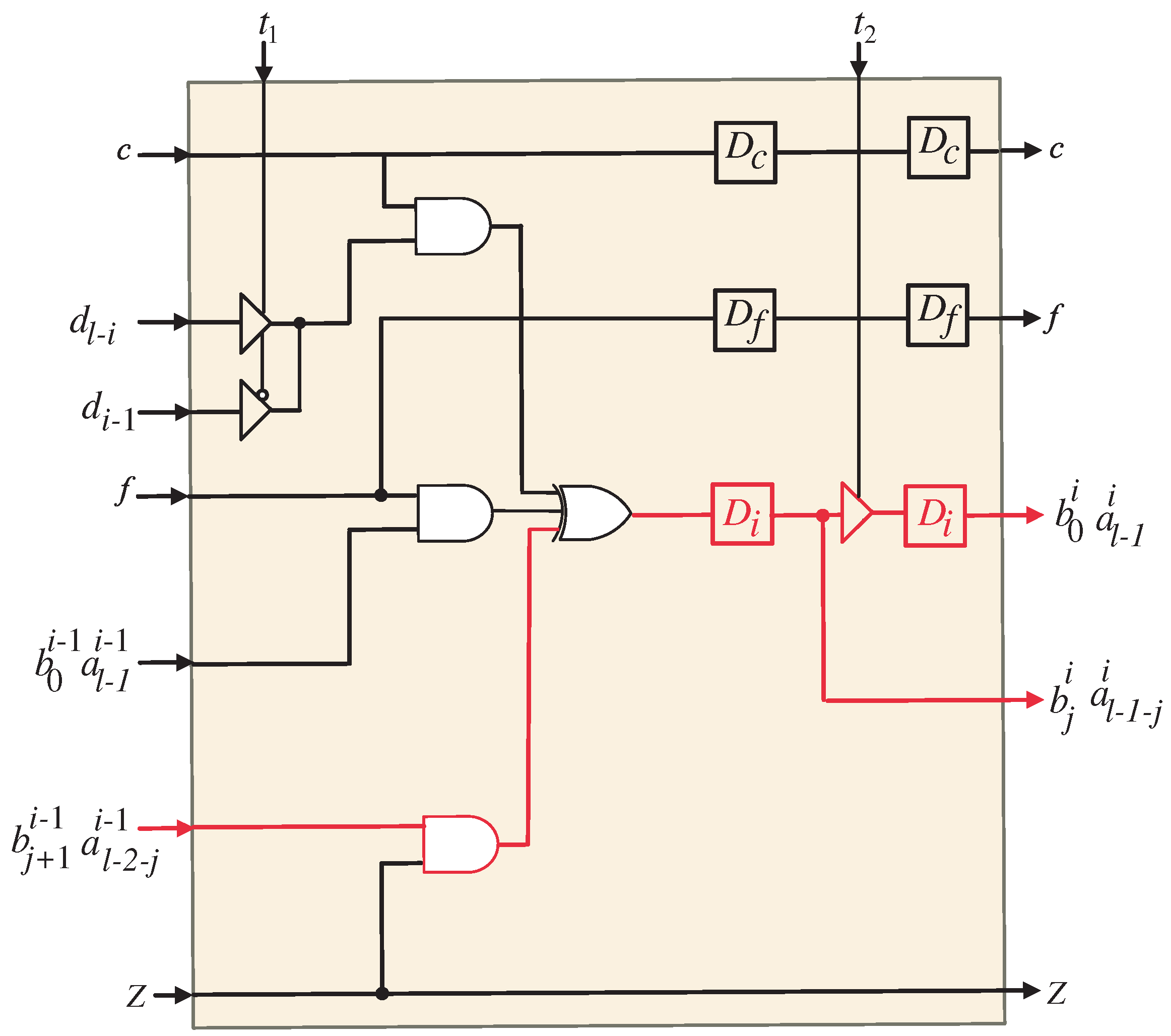
The semi-systolic array structure resulting from the application of the projection function () to the DG is presented in Figure 3. This configuration represents a serial in–serial out (SISO) system, wherein data are processed sequentially. The SISO framework consists of a unified datapath that facilitates the computation of coefficients A and B using the same set of processing elements (PEs). The processor structure comprises PEs, making it scalable for different problem sizes. The generation of the final output (P) requires a total of clock cycles, which reflects the inherently sequential nature of the computation. In the proposed SISO structure, the first and last PEs, as illustrated in Figure 4 and Figure 5, respectively, possess specialized logic structures that differ slightly from those employed in the intermediate PEs (Figure 6). This distinction arises from the need to handle input elements of coefficients A and B and ensure the proper generation of their respective output bits. The proposed SISO configuration offers an efficient approach for sequential data processing, employing a unified datapath and carefully designed PEs to achieve accurate results within the defined number of clock cycles.
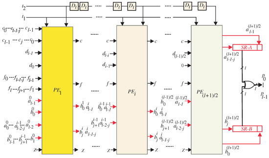
Figure 3.
Suggested SISO systolic multiplier.

Figure 4.
PE1 logic circuit of the systolic array. The square blocks represent D-latches.
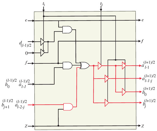
Figure 5.
logic circuit of the systolic array. The square blocks represent D-latches.
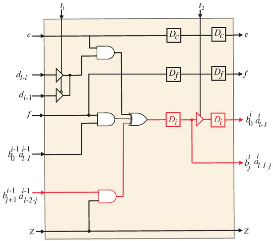
Figure 6.
logic circuit of the systolic array. The square blocks represent D-latches.
The coefficients of output A, denoted as , where , are generated by the processor array in a serial manner. These coefficients are produced by the last PE and stored in the upper shift register depicted in Figure 3. Similarly, the coefficients of output B, represented as , , are serially generated by the last PE and stored in the lower shift register shown in the same figure.
It is worth noting that bits and are stored in flip-flops within the PEs to ensure the proper computation of coefficients A and B. Consequently, these bits have a separate serial bus from the remaining coefficient bits, as indicated in Figure 3. Furthermore, the resulting bits ( and ) from the last PE are stored in separate flip-flops distinct from the output shift registers, as depicted in Figure 3. This separation is essential to maintain the correct order of the resulting coefficient bits and prevent any disordering. In order to produce the end-result P, the relevant bits of coefficients A and B need to be XORedtogether, as illustrated in Figure 3.
Upon examining the SISO systolic structure, the assignment of input signals and to their corresponding PEs can be observed. Furthermore, intermediate signals , , , , , and are pipelined across neighboring PEs.
It is important to note that there exists a time difference of l time instances between the application of signals and to the inputs of the PEs. Similarly, the same time difference is observed when signals and are applied to the PE inputs. This time difference of l time instances enables the proper synchronization and coordination of the computations within the SISO structure, ensuring accurate and sequential data processing.
The tri-state buffers at the input of the first PE (Figure 4) are controlled by control signal to select between the inputs required to compute the coefficients of A and B. Through the first l time steps, control signal activates () to pass the input elements required to compute the coefficients of A in sequence. Starting from time step l to time step , the control signal () deactivates () to pass the input elements required to compute the coefficients of B. Also, this control signal is used in the remaining PEs to activate and deactivate the tri-state buffers at their inputs to select between and signals. The tri-state buffers shown at the output of the last PE (Figure 5) are controlled using to pass the output bits(, , , and ) at the proper time. Signals , are passed through the deactivation interval of control signal and signals and are passed through the activation interval of this control signal ().
At the second and time instances, control signal activates () to enable the tri-state buffer shown at the output of the first PE (PE1, Figure 4) to hold the MSB of A () and the LSB of B, (). These signals should be utilized in the subsequent PE through the following l time steps. The control signal () should be delayed by two time instances before being assigned to each PE. This delay makes it possible for the tri-state buffers to store the updated MSBs of A () and the LSBs of B () in the corresponding PEs at the appropriate time instances. In order to achieve the required delay, control signal should be pipelined through the D-latches shown in Figure 3. Before the SISO structure begins to operate, it is important to note that all D-latches must be cleared.
The functioning of the SISO framework can be summarized in the following way:
- Through the first l time instances ( to ), control signal activates () to pass input signals , , , , and in sequence to the first PE (PE1). Also, through these time instances, input signals , , and are allocated to all PEs. The coefficients of variable A are computed using each of these signals.
- Through time instances to , control signal deactivates () to pass input signals , , and to the first PE (PE1). Input signals , , and are also allocated to all PEs during this time period. To calculate the coefficients of variable B, all of these signals should be used.
- Through time instances (), , control signal activates () to enable the corresponding tri-state buffer in each PE to hold the MSBs of A () to be allocated to the next PE.
- Through time instances (), , control signal activates () to enable the corresponding tri-state buffer in each PE to hold the LSBs of B () to be allocated to the next PE.
- Starting from time instance l, the resulting coefficients of variable A start to present at the output of the last PE, one bit at a time. At time instance , all the coefficients of A will be stored in the upper shift register shown at the right of Figure 3. It is worth noting that control signal deactivates () through intervals l to to enable the active low tri-state buffers to pass the coefficients of variable A.
- Starting from time instance , the resulting coefficients of variable B start to present at the output of the last PE, one bit at a time. At time instance , all the coefficients of B will be stored in the lower shift register shown at the right of Figure 3. Also at this time instance, the corresponding bits of the A and B coefficients are applied to two-input XOR gates (l two-input XOR gates) to obtain the final product bits of P, , , as indicated in Figure 3. It is important to note that control signal activates () through the time intervals to in order to allow the active high tri-state buffers to pass the coefficients of variable B.
6. Results and Discussions
The suggested SISO systolic multiplier structure is compared to previously reported competing layouts such as bit-serial systolic and non-systolic multiplier schemes [11,12,17,18,19,22,41,42]. The comparison results are collected in Table 1, taking into account criteria such as total gate counts, latency, and critical path delay (CPD).

Table 1.
Comparison between the offered multiplier arrangement and other bit-serial systolic multipliers in terms of space and delay overhead.
In Table 1, the symbols , , , and reflect the latencies of various logic components, tri-state Buffers, two-input AND gates, two-input XOR gates, and 2-to-1 MUXs. These latencies have a substantial impact on the overall performance and efficiency of multiplier designs.
By examining the adopted area and delay design metrics and comparing them with the rival architectures, a comprehensive evaluation can be conducted to assess the advantages and disadvantages of the proposed SISO systolic multiplier layout. This analysis provides valuable insights into the relative strengths and weaknesses of different multiplier designs, aiding in the selection of the most suitable architecture for specific applications.
When analyzing the area and delay complexity estimates presented in Table 1, it is crucial to consider that only a small portion of the multiplier configurations mentioned in [18,41] are systolic or semi-systolic in nature. These studies describe designs based on two types of irreducible polynomials, namely trinomials and -nomials (irreducible polynomials with non-zero terms). Among these, the trinomial-based solutions outperform the -nomial solutions. Therefore, for the purpose of comparison, the analysis focuses on evaluating the trinomial-based structures alongside the proposed multiplier configuration.
The proposed multiplier arrangement has multiple benefits based on the projected findings reported in Table 1. It has a much smaller gate count, with AND gates, XOR gates, 0 MUXs, and D-latches. On the other hand, it has a moderate number of tri-state buffers, with a total of buffers. As a whole, the proposed multiplier framework has a substantially lower gate count than the competing ones.This detailed breakdown of the gate count clearly demonstrates the superiority of the suggested multiplier arrangement in terms of gate utilization. The proposed layout achieves a substantially lower gate count compared to existing architectures. By reducing the number of gates, the proposed arrangement offers improved space efficiency and more effective utilization of available resources.
The advantages of the proposed multiplier arrangement in terms of gate count have significant implications. The reduced gate count not only contributes to a smaller physical footprint but also offers potential benefits such as lower power consumption and improved performance. Furthermore, the optimized gate count aligns well with the resource constraints typically encountered in IoT applications, where devices often have limited resources and space availability.
Acknowledging the significance of other multiplier constructions is essential in providing a comprehensive analysis. In the context of the non-systolic multiplier constructions mentioned in [18,41], it is important to note that while these constructions may have lower latency compared to the recommended design, they suffer from significantly higher critical path delay (CPD). This indicates that although they may offer faster processing times, they are constrained by longer delays in critical paths, which can impact overall performance. In contrast, the Fenn multiplier [12] demonstrates similar latency and CPD to the proposed multiplier layout. This suggests that both designs achieve comparable processing times and exhibit similar delay characteristics in their critical paths. As a result, the Fenn multiplier can be considered a viable alternative to the suggested multiplier arrangement, offering similar performance without compromising on critical path delays.
Considering these factors, the choice between the recommended multiplier layout and other constructions depends on the specific requirements and priorities of the application. If minimizing latency is the primary concern, the non-systolic multiplier constructions mentioned in [18,41] may be preferable. However, if striking a balance between latency and critical path delay is important, both the suggested multiplier arrangement and the Fenn multiplier [12] can be considered as suitable options.
Indeed, it is essential to consider Ibrahim’s multiplier structure [19] in the comparison. According to the available information, Ibrahim’s design exhibits a latency of approximately (), which suggests that it may offer faster processing times compared to the proposed architecture. However, it is worth noting that Ibrahim’s design also has a larger critical path delay (CPD) due to additional delays introduced by the MUX components.
It is important to acknowledge that these comparisons are based on theoretical analysis and the reported latency and CPD values. To validate the actual performance of these designs, practical implementation and extensive testing would be necessary. Factors such as circuit layout, technology-specific characteristics, and other implementation-dependent considerations could impact the real-world performance of these multiplier architectures. Therefore, while the theoretical comparisons provide valuable insights, it is crucial to conduct practical experiments and evaluations to determine the true performance and efficiency of these designs in real-world scenarios. Such empirical validation would provide a more accurate understanding of the strengths and limitations of each multiplier architecture.
To validate the observations presented in Table 1, a comprehensive assessment of the different architectural designs was conducted. The evaluation focused on the following three key aspects: the overall area (A), the entire processing time (T), and the area–time (AT) trade-off. To ensure accurate estimations, the assessment utilized the NanGate Open Cell Library, specifically the 15 nm technology node operating at a voltage of 0.8V. This choice of library enabled precise determination of the area (total gate count) and delay for each critical logic component in the multiplier architectures under evaluation.
The approach of assessing the area of each basic component (R) by utilizing the two-input NAND gate as a reference is a valuable strategy for conducting a comparative analysis of the area efficiency of the different multiplier structures. Using the two-input NAND gate as a reference allows for a standardized measurement of the area requirements of each component. By obtaining the area values for each component in the multiplier architectures under evaluation, a comprehensive view of the overall area requirements for each design can be gained. This information is crucial in understanding the trade-offs between different architectures in terms of area efficiency and space utilization.
The evaluation outcomes for each component can be summed up as listed below:
- Tri-state buffer: The area () of the tri-state buffer component is approximately 0.8 units, and it has a delay () of around 7.9 picoseconds;
- Two-input AND gate: The area () of the two-input AND gate component is approximately 1.2 units, and it has a delay () of around 11.3 picoseconds;
- Two-input XOR gate: The area () of the two-input XOR gate component is approximately 2.5 units, and it has a delay () of around 12.7 picoseconds;
- 2-to-1 MUX: The area () of the 2-to-1 MUX component is approximately 2.5 units, and it has a delay () of around 12.4 picoseconds;
- D-latch: The area () of the D-latch component is approximately 2.8 units, and it has a delay () of around 16.6 picoseconds.
Indeed, the obtained results regarding the area and delay characteristics of each component offer valuable insights into the overall performance of the different multiplier architectures. These characteristics play a crucial role in determining the efficiency, resource utilization, and speed of the multiplier designs.
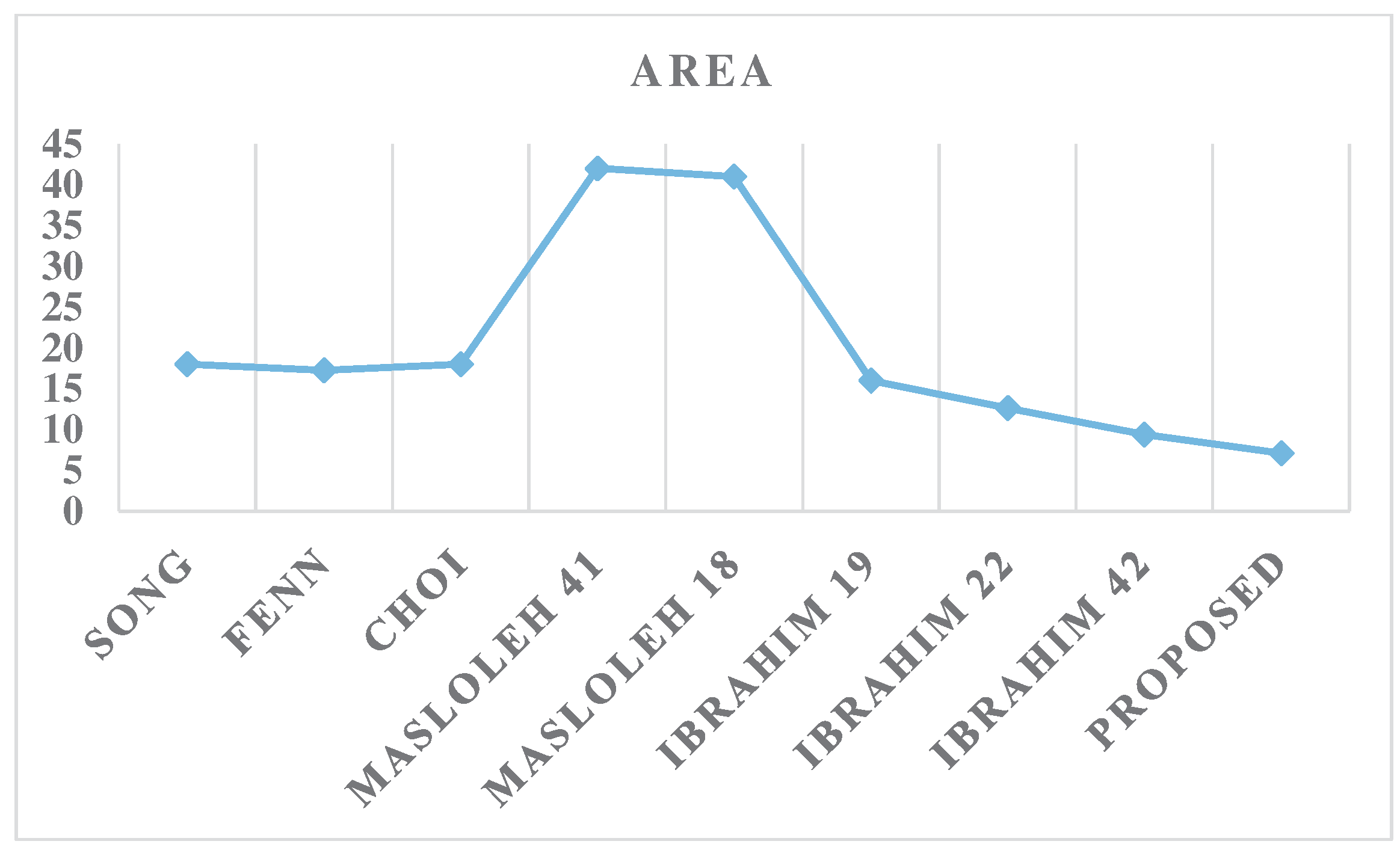
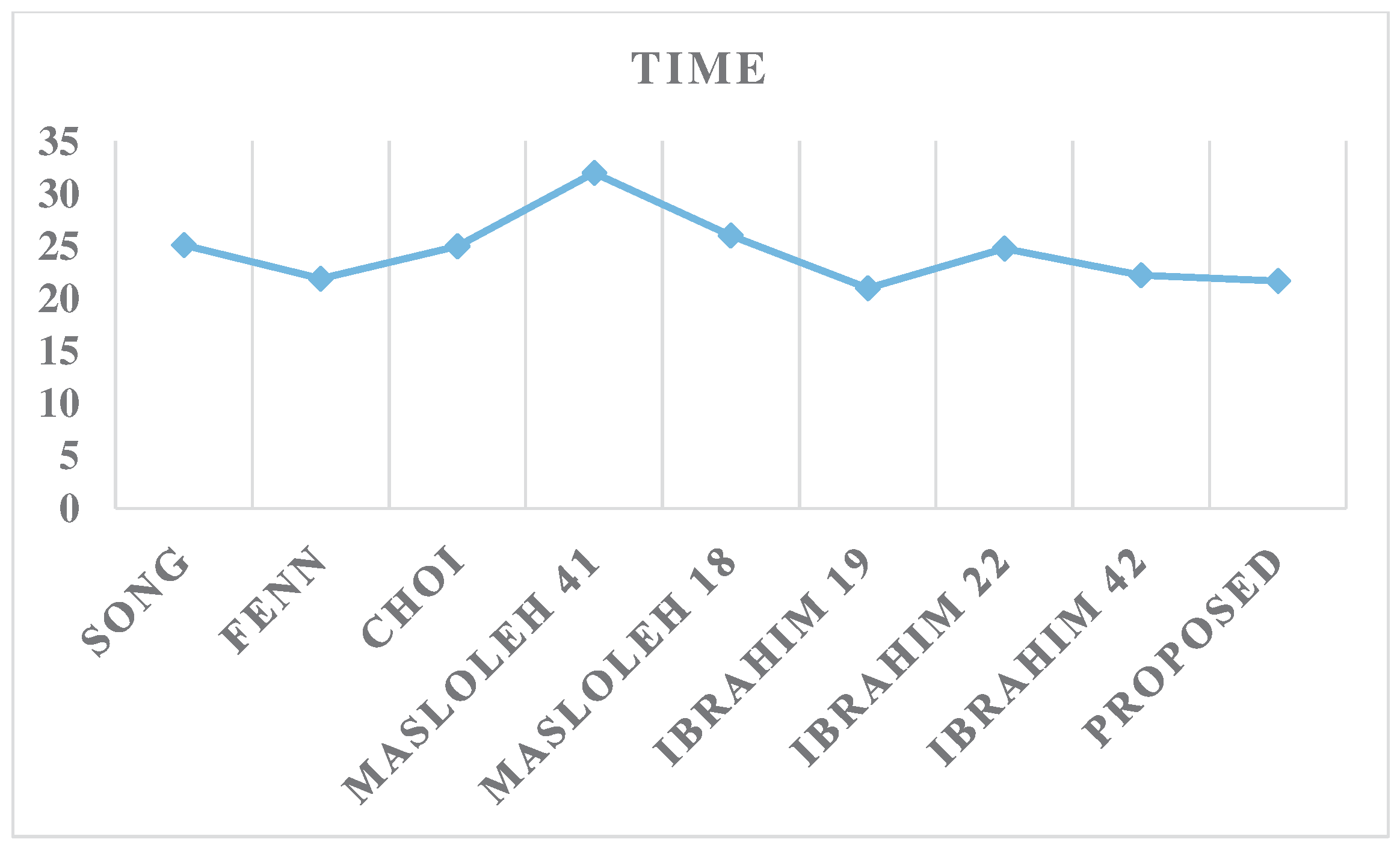
The results presented in Table 2 clearly demonstrate the significant advantages of the proposed SISO systolic array multiplier construction over recently reported proficient bit-serial multiplier constructions. These advantages are particularly evident when considering the metrics of area (A) and area–time (AT) product, which are crucial factors in assessing the performance and efficiency of multiplier designs.
Table 2.
Time- and space-related costs associated with serial constructions for and .
An analysis of the results presented in Table 2 and Figure 7 reveals that the proposed design achieves significantly better area efficiency compared to the competitor designs. Specifically, the proposed solution outperforms the other approaches by at least 24.5%. However, when examining the time performance metric in Table 2 and Figure 8, the design proposed in [22] is observed to marginally outperform the current proposal by 3.2%. However, this competitor design incurs a much larger area overhead in comparison to the proposed solution.
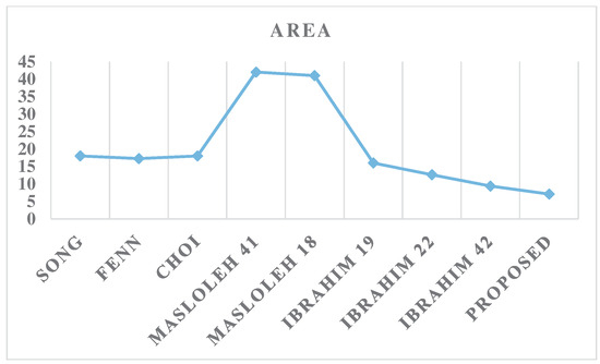
Figure 7.
Area results.
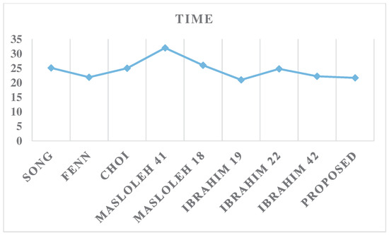
Figure 8.
Time results.
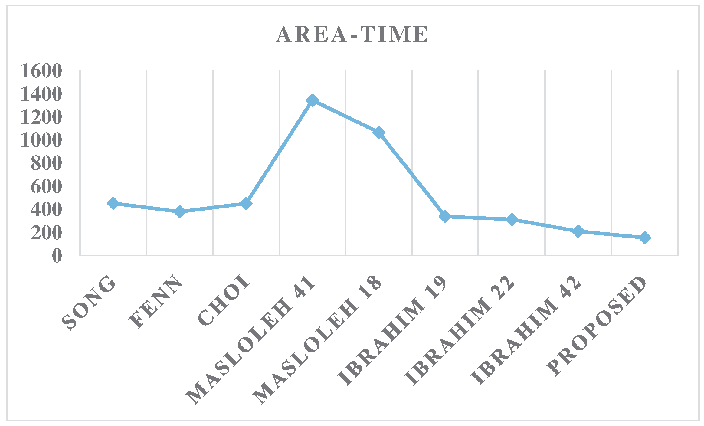
Since the proposed design exhibits a mix of strengths and weaknesses when examined separately in terms of area and time performance, it is essential to assess the designs using the combined area–time (AT) metric to obtain a comprehensive evaluation. As demonstrated by the data presented in Table 2 and Figure 9, the proposed design achieves a significantly superior AT result, outperforming the competing designs by a margin of at least 26.2%.
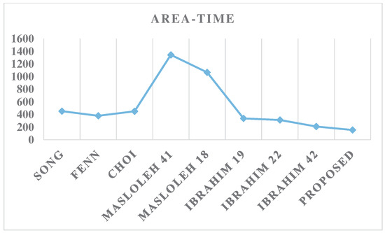
Figure 9.
Area–time results.
The comprehensive analysis across the key performance indicators of area, time, and the composite AT metric firmly establishes the overall advantages of the proposed design compared to the existing alternatives. The substantial improvements in area efficiency, coupled with the competitive AT performance, solidify the proposed SISO systolic array multiplier as the preferred solution.
These improvements indicate that the proposed design, which incorporates the concept of symmetry, achieves a significant enhancement in area, resulting in a more compact and space-efficient implementation. By leveraging symmetrical properties, such as balanced arrangements and repeated patterns, the design optimizes resource utilization and reduces the required area for the multiplier. This reduction in area brings advantages such as lower manufacturing costs, improved integration within larger systems, and better accommodation in resource-constrained environments typical of MIoT endpoints. Moreover, the improvement in the area–time product demonstrates a balanced approach between computational performance and resource utilization. The design offers faster processing times while maintaining efficient area utilization, effectively optimizing the trade-off between performance and resource requirements. These findings strongly support the suitability of the proposed architecture for MIoT applications, as it effectively reduces both the area and area–time product, addressing the constraints of limited resources and space complexity. Thus, the design meets the needs of resource-limited MIoT devices by leveraging the benefits of symmetry and optimizing resource utilization.
7. Summary and Conclusions
This paper introduces a new SISO systolic array design, leveraging the concept of symmetry, for the application of the Montgomery modular multiplication algorithm over GF(). The suggested architecture exhibits regular processing element builds and localized interconnections, making it well-suited for VLSI implementations. Compared to existing multiplier architectures, the proposed design offers several advantages. It achieves efficient resource utilization by reducing area overhead while maintaining a respectable delay, resulting in a more compact implementation compared to its competitors. The compactness of the design enables its integration into resource-constrained MIoT devices, providing the necessary computational capabilities for secure cryptographic operations. By incorporating symmetry, the proposed architecture strikes a balance between efficient resource utilization and computational performance, addressing the constraints of resource-limited MIoT devices and reinforcing its suitability for MIoT applications. The forthcoming research will concentrate on the practical hardware realization of the proposed solution. This tangible exploration will offer vital information about the viability and performance of the suggested strategy in actual deployment settings.
Author Contributions
Conceptualization, A.I.; methodology, A.I. and F.G.; software, A.I.; validation, A.I.; formal analysis, A.I.; investigation, A.I.; resources, A.I.; data curation, A.I.; writing—original draft preparation, A.I.; writing—review and editing, A.I. and F.G.; visualization, A.I.; supervision, A.I.; project administration, A.I.; funding acquisition, A.I. All authors have read and agreed to the published version of the manuscript.
Funding
This research was funded by Prince Sattam bin Abdulaziz University project number (PSAU/2024/01/29201).
Data Availability Statement
Data are contained within the article.
Acknowledgments
The authors extend their appreciation to Prince Sattam bin Abdulaziz University for funding this research work through project number (PSAU/2024/01/29201).
Conflicts of Interest
The authors declare no conflicts of interest.
Abbreviations
The following abbreviations are used in this manuscript:
| MIoT | Medical Internet of Things |
| GF | Galois Field |
| PE | Processing Element |
| ECC | Elliptic Curve Cryptography |
| DG | Dependency Graph |
| AT | Area-Time |
| AOP | All-One Polynomial |
| PB | Polynomial Basis |
| NB | Normal Basis |
| DB | Dual Basis |
| ESP | Equally Spaced Polynomials |
| MMM | Montgomery Modular Multiplication |
| VLSI | Very Large Scale Integrated Circuit |
| SISO | Serial-In/Serial-Out |
| CPD | Critical Path Delay |
References
- Kumar, M.; Kumar, A.; Verma, S.; Bhattacharya, P.; Ghimire, D.; Kim, S.-H.; Hosen, A.S. Healthcare internet of things (h-iot): Current trends, future prospects, applications, challenges, and security issues. Electronics 2023, 12, 2050. [Google Scholar] [CrossRef]
- Pons, M.; Valenzuela, E.; Rodríguez, B.; Nolazco-Flores, J.A.; Del-Valle-Soto, C. Utilization of 5g technologies in iot applications: Current limitations by interference and network optimization difficulties—A review. Sensors 2023, 23, 3876. [Google Scholar] [CrossRef]
- Varga, P.; Peto, J.; Franko, A.; Balla, D.; Haja, D.; Janky, F.; Soos, G.; Ficzere, D.; Maliosz, M.; Toka, L. 5 g support for industrial iot applications—challenges, solutions, and research gaps. Sensors 2020, 20, 828. [Google Scholar] [CrossRef]
- Rayan, R.A.; Tsagkaris, C.; Iryna, R.B. The internet of things for healthcare: Applications, selected cases and challenges. IoT Healthc. Ambient. Living 2021, 1–15. [Google Scholar]
- Elhoseny, M.; Thilakarathne, N.N.; Alghamdi, M.I.; Mahendran, R.K.; Gardezi, A.A.; Weerasinghe, H.; Welhenge, A. Security and privacy issues in medical internet of things: Overview, countermeasures, challenges and future directions. Sustainability 2021, 13, 11645. [Google Scholar] [CrossRef]
- Pöpper, C. Applied cryptography and network security. In Proceedings of the 22nd International Conference, ACNS 2024, Abu Dhabi, United Arab Emirates, 5–8 March 2024; Proceedings, Part I. Springer Nature: Berlin/Heidelberg, Germany, 2024. [Google Scholar]
- Tang, Q. Public-key cryptography—PKC 2024. In Proceedings of the 27th IACR International Conference on Practice and Theory of Public-Key Cryptography, Sydney, NSW, Australia, 15–17 April 2024; Proceedings, Part II. Springer: Cham, Switzerland, 2024. [Google Scholar]
- Seedorf, J.; Mazhar, K.; Schwabe, F.; Omerovic, I. Applied cryptography in the internet-of-things. In Online-Labs in Education; Nomos Verlagsgesellschaft mbH & Co. KG: Baden, Austria, 2022; pp. 361–374. [Google Scholar]
- Haa, J.-C.; Moon, S.-J. A common-multiplicand method to the montgomery algorithm for speeding up exponentiation. Inf. Process. Lett. 1998, 66, 105–107. [Google Scholar] [CrossRef]
- Lee, K.-J.; Yoo, K.-Y. Linear systolic multiplier/squarer for fast exponentiation. Inf. Process. Lett. 2000, 76, 105–111. [Google Scholar] [CrossRef]
- Song, L.; Parhi, K.K. Efficient finite field serial/parallel multiplication. In Proceedings of the IEEE 1996 International Conference on Application-Specific Architectures and Processors, Chicago, IL, USA, 19–23 August 1996; pp. 72–82. [Google Scholar]
- Fenn, S.T.J.; Taylor, D.; Benaissa, M. A dual basis bit serial systolic multiplier for gf(2m). Integr. VLSI J. 1995, 18, 139–149. [Google Scholar] [CrossRef]
- Chiou, C.-W.; Lee, C.-Y.; Deng, A.-W.; Lin, J.-M. Concurrent error detection in montgomery multiplication over GF(2m). IEICE Trans. Fundam. Electron. Commun. Comput. Sci. 2006, E89-A, 566–574. [Google Scholar]
- Huang, W.T.; Chang, C.; Chiou, C.; Chou, F. Concurrent error detection and correction in a polynomial basis multiplier over GF(2m). IET Inf. Secur. 2010, 4, 143–150. [Google Scholar] [CrossRef]
- Kim, K.W.; Jeon, J.C. Polynomial basis multiplier using cellular systolic architecture. IETE J. Res. 2014, 60, 194–199. [Google Scholar] [CrossRef]
- Kim, K.W.; Jeon, J.C. A semi-systolic montgomery multiplier over GF(2m). IEICE Electron. Express 2015, 12, 20150769. [Google Scholar] [CrossRef]
- Choi, S.; Lee, K. Efficient systolic modular multiplier/squarer for fast exponentiation over GF(2m). IEICE Electron. Express 2015, 12, 20150222. [Google Scholar] [CrossRef]
- Abdulrahman, E.A.; Reyhani-Masoleh, A.H. High-speed hybrid-double multiplication architectures using new serial-out bit-level mastrovito multipliers. IEEE Trans. Comput. 2016, 65, 1734–1747. [Google Scholar] [CrossRef]
- Ibrahim, A. Novel bit-serial semi-systolic array structure for simultaneously computing field multiplication and squaring. IEICE Electron. Express 2019, 16, 20190600. [Google Scholar] [CrossRef]
- Kim, K.W.; Lee, J.D. Efficient unified semi-systolic arrays for multiplication and squaring over GF(2m). IEICE Electron. Express 2017, 14, 20170458. [Google Scholar] [CrossRef]
- Kim, K.W.; Kim, S.H. Efficient bit-parallel systolic architecture for multiplication and squaring over GF(2m). IEICE Electron. Express 2018, 15, 20171195. [Google Scholar] [CrossRef]
- Ibrahim, A. Efficient parallel and serial systolic structures for multiplication and squaring over GF(2m). Can. J. Electr. Comput. Eng. 2019, 42, 114–120. [Google Scholar] [CrossRef]
- Hsu, I.S.; Truong, T.K.; Deutsch, L.J.; Reed, I. A comparison of vlsi architecture of finite field multipliers using dual, normal, or standard bases. IEEE Trans. Comput. 1988, 37, 735–739. [Google Scholar] [CrossRef]
- Wu, H. Bit-parallel finite field multiplier and squarer using polynomial basis. IEEE Trans. Comput. 2002, 51, 750–758. [Google Scholar]
- Lee, C.-Y. Low-latency bit-pararallel systolic multiplier for irreducible xm + xn + 1 with GCD(m, n) = 1. IEICE Trans. Fund. Electron. Commun. Comput. Sci. 2008, 55, 828–837. [Google Scholar]
- Ting, Y.-R.; Lu, E.-H.; Lu, Y.-C. Ringed bit-parallel systolic multipliers over a class of fields GF(2m). Integr. VLSI J. 2005, 38, 371–384. [Google Scholar] [CrossRef]
- Fournaris, A.P.; Koufopavlou, O. Versatile multiplier architectures in gf(2k) fields using the montgomery multiplication algorithm. Integr. VLSI J. 2008, 41, 571–578. [Google Scholar] [CrossRef]
- Kim, K.-W.; Lee, H.-H.; Kim, S.-H. Efficient combined algorithm for multiplication and squaring for fast exponentiation over finite fields GF(2m). In Proceedings of the 7th International Conference on Emerging Databases, LNEE, Gifu, Japan, 3–5 July 2017; Volume 461, pp. 50–57. [Google Scholar]
- Kitsos, P.; Theodoridis, G.; Koufopavlou, O. An efficient reconfigurable multiplier architecture for galois field GF(2m). Microelectron. J. 2003, 34, 975–980. [Google Scholar] [CrossRef]
- Selimis, G.N.; Fournaris, A.P.; Michail, H.E.; Koufopavlou, O. Improved throughput bit-serial multiplier for GF(2m) fields. Integr. VLSI J. 2009, 42, 371–384. [Google Scholar] [CrossRef]
- Guo, J.-H.; Wang, C.-L. Digit-serial systolic multiplier for finite fields GF(2m). IEEE Proc. Comput. Digital Tech. 1998, 145, 143–148. [Google Scholar] [CrossRef]
- Hutter, M.; Grobschald, J.; Kamenje, G.-A. A versatile and scalable digit-serial/parallel multiplier architecture for finite fields gf(2m). In Proceedings of the 2003 4th International Conference on Information Technology: Coding and Computing (ITTCC2003), Las Vegas, NV, USA, 28–30 April 2003; pp. 692–700. [Google Scholar]
- Song, L.; Parhi, K.K. Low-energy digit serial/parallel finite field multipliers. J. Vlsi Signal Process. Syst. 1998, 19, 149–166. [Google Scholar] [CrossRef]
- Kim, C.H.; Hong, C.P.; Kwon, S. A digit-serial multiplier for finite field GF(2m). IEEE Trans. Very Large Scale Integr. Syst. 2005, 13, 476–483. [Google Scholar]
- Hariri, A.; Reyhani-Masoleh, A. Digit-serial structures for the shifted polynomial basis multiplication over binary extension fields. In Proceedings of the LNCS International Workshop Arithmetic of Finite Fields (WAIFI), Rennes, France, 6–8 July 2008; pp. 103–116. [Google Scholar]
- Lee, K. Low Complexity Systolic Montgomery Multiplication over Finite Fields GF(2m). J. Korea Soc. Digit. Ind. Inf. Manag. 2022, 18, 1–9. [Google Scholar]
- Lee, K. Resource and Delay Efficient Polynomial Multiplier over Finite Fields GF(2m). J. Korea Soc. Digit. Ind. Inf. Manag. 2020, 16, 1–9. [Google Scholar]
- Gebali, F. Algorithms and Parallel Computers; John Wiley: New York, NY, USA, 2011. [Google Scholar]
- Ibrahim, A.; Elsimary, H.; Gebali, F. New systolic array architecture for finite field division. IEICE Electron. Express 2018, 15, 20180255. [Google Scholar] [CrossRef]
- Ibrahim, A. Scalable digit-serial processor array architecture for finite field division. Microelectron. J. 2019, 85, 83–91. [Google Scholar] [CrossRef]
- Reyhani-Masoleh, A. A new bit-serial architecture for field multiplication using polynomial bases. In Proceedings of the 7th International Workshop Cryptographic Hardware Embedded Systems (CHES 2008), Washington, DC, USA, 10–13 August 2008; pp. 300–314. [Google Scholar]
- Ibrahim, A. Low-space bit-serial systolic array architecture for interleaved multiplication over GF(2m). IET Comput. Digit. Tech. 2021, 15, 223–229. [Google Scholar] [CrossRef]
Disclaimer/Publisher’s Note: The statements, opinions and data contained in all publications are solely those of the individual author(s) and contributor(s) and not of MDPI and/or the editor(s). MDPI and/or the editor(s) disclaim responsibility for any injury to people or property resulting from any ideas, methods, instructions or products referred to in the content. |
© 2024 by the authors. Licensee MDPI, Basel, Switzerland. This article is an open access article distributed under the terms and conditions of the Creative Commons Attribution (CC BY) license (https://creativecommons.org/licenses/by/4.0/).