Article

A Virtual Synchronous Generator-Based Control Strategy and Pre-Synchronization Method for a Four-Leg Inverter under Unbalanced Loads

1
The School of Electrical Engineering, Shandong University, Jinan 250061, China
2
The School of Rail Transportation, Shandong Jiaotong University, Jinan 250357, China
*
Author to whom correspondence should be addressed.
Symmetry 2024, 16(9), 1116; https://doi.org/10.3390/sym16091116
Submission received: 16 July 2024 / Revised: 15 August 2024 / Accepted: 23 August 2024 / Published: 28 August 2024

Abstract

:
Virtual synchronous generator (VSG) control has positive effects on the stability of microgrids. In practical power systems, both single-phase loads and three-phase unbalanced loads are present. The four-leg inverter is an alternative solution for the power supply of unbalanced loads and grid connections. The traditional VSG control strategy still faces challenges when using a four-leg inverter to provide a symmetrical voltage and stable frequency in the load power supply and pre-synchronization. This paper proposes a VSG-based control strategy along with a pre-synchronization method for four-leg inverters. An improved VSG control strategy is put forward for four-leg inverters. The improved virtual impedance control and power calculation methods are integrated into the control loop to suppress the voltage asymmetry and frequency ripples. Building on the improved VSG control strategy, a pre-synchronization control approach is proposed to minimize the amplitude and phase angle discrepancies between the inverter output voltage and the power grid voltage. In addition, an optimized design method for control parameters is presented to improve VSG dynamic performance. A hardware prototype of the four-leg inverter is built; the results show that the voltage unbalance ratio can be reduced by 89%, and the response time can be shortened by 50%.

1. Introduction

The advancement of renewable energy and power electronics has facilitated the development of microgrids [1,2,3,4]. The microgrid is capable of operating in either isolated mode or grid-connected mode. The stability of microgrids is challenged by the intermittency and uncertainty of renewable energy generation, as well as the lack of inertia and damping in power electronic converters [5]. The virtual synchronous generator (VSG) has been widely implemented in microgrids [6]. Much research work focuses on the parameter design of VSG. Paper [7] proposes an adaptive virtual inertia that integrates the benefits of both large and small inertia. In addition, in [8], the adaptive virtual inertia and damping coefficient can be used to improve the output during disturbances in the system, which also enhances the dynamic stability of VSG. Particle swarm optimization (PSO) is used in the optimization design of parameters and virtual impedance to enhance the stability of microgrids [9]. Frequency regulation is of great importance to the reliability of microgrids. Since the development of electric vehicles can lead to frequency instability in microgrids, an VSG based frequency control strategy is put forward in [10] to coordinate the demand between the user charging and grid frequency control. Model predictive control (MPC) is integrated into the VSG control loop, which can keep dynamic change to the reference value of the power [11]. In [12], all control loops are replaced with MPC to improve frequency regulation capability further. Moreover, a control method is proposed to enhance the stability of paralleled synchronous generator and virtual synchronous generator [13]. In recent years, most studies on VSG relate to parameter design and control strategies under balanced conditions. Even if the fault is considered, it is mostly considered balanced fault [14]. There are few studies on VSG control under unbalanced conditions. An improved VSG control strategy under imbalanced grid voltage is proposed in [15], which can improve the dynamic performance. In addition, the proposed control strategy makes the output current balanced or active and reactive power constant.
In practical power supply systems, load asymmetry is quite common because of the single-phase loads or asymmetrical three-phase loads. As for the unbalanced load power supply with VSG, there are two considerations: (1) basically, the converter with a grid-forming control strategy can be considered as a voltage source. The symmetrical three-phase voltages need to be provided first. It is different from the converter with grid-following control, which aims to maintain a symmetrical current or power [16,17]. (2) With load asymmetry, the power supply system is in a normal operating state rather than a fault condition.
There is no neutral connection, so a traditional converter with six switches is unable to make the three-phase voltages balanced under unbalanced load. A three-phase four-wire topology is proposed, which can provide the neutral connection [18,19,20,21]. A common way is to add a Dyn transformer after the filter [18]. The fourth wire is connected to the grid side of the transformer instead of the converter. A converter with a four-wire topology has no ability to control zero-sequence voltages directly, due to the Dyn connection of transformers. Topologies that utilize split DC link capacitors are commonly employed to provide a neutral connection [19,20,21]. The neutral point of the AC filter capacitors is connected to the midpoint of the two split DC-link capacitors. Due to the topology involving split DC link capacitors, the zero-sequence current flows through the capacitor, causing a voltage ripple. Thus, large capacity capacitors are required to suppress the voltage ripple.
The topology of a four-leg inverter is presented in [22] for the power supply of an unbalanced load. The modulation method is the key to four-leg inverters. In the process of modulation by a two-dimensional space vector, the sum of base vector is not zero due to the unbalanced output voltages. A three-dimensional space vector modulation (3D-SVM) is introduced, according to the balanced neutral potential [23,24,25]. A carrier-based PWM modulation is put forward in [26]. The fourth leg is modulated independently by calculating the offset zero-sequence voltage. This approach allows for the decoupling of the fourth leg from the other three legs, thereby reducing implementation complexity. In [27], a new carrier-based modulation strategy is put forward for a Z-source three-level four-leg inverter to reduce the leakage of current, which has good fault-tolerance deal capability. The Z-source three-level four-leg inverter is used for its ability to address imbalance problems. The above studies are aimed at voltage source inverters, and the 3D-SVM for four-leg current source inverters was first presented in [28].
In addition to the modulation methods, extensive research has been conducted on control strategies for four-leg converters, with a novel control scheme introduced in [29]. Proportional integral (PI) control is adopted for the main controller, and proportional-resonant (PR) control is used for the fourth-leg controller. The output voltages can be symmetrical under unbalanced nonlinear loads. A resonant-filter-bank controller is used to provide balanced output voltages in [30]. A set of PR controllers are designed to output accurate fundamental voltage and suppress dominant harmonic voltages. High steady-state and dynamic performance can be obtained with the proposed controllers. To obtain better steady-state and dynamic performance, nonlinear control methods are also studied for the four-leg inverter [31,32,33,34,35]. The nonlinear control methods include sliding-mode control [31], model predictive control [32,33], a deadbeat controller [34], and flatness-based grey wolf control [35]. The control results can be guaranteed even in the case of parameter mismatch [31,32,33,34,35]. In addition, VSG are integrated into the control loop of the four-leg inverter for frequency and voltage adjustment [36]. The abovementioned studies are shown in Table 1. Table 1 shows the advantages and disadvantages of different control strategies for a four-leg inverter.
At present, most of the papers relating to four-leg converters focus on modulation and control methods. Few studies focus on control strategy combined with inertia and damping. In [37], an adaptive supplementary control for the VSG, based on virtual impedance, is proposed to reduce the output voltage error. However, the output voltages are not balanced, which is caused by the limitations of the converter topology. Paper [36] applies a four-leg converter to VSG. An adaptive PR control method is proposed as the inner control loop of VSG. However, the research is limited, as the controller and power process design are based on load balance. Although the control method is improved, it cannot output balanced voltages and stable frequency. Moreover, the influence of virtual impedance and parameters on VSG is not considered [38]. Hence, a deep study is carried out in this paper. The key contributions are summarized as follows:
(1)
An improved VSG control strategy for a four-leg inverter is proposed. The improved virtual impedance control and power calculation method are used to keep the output voltages symmetrical and stable in the case of load symmetry. The results show that the voltage unbalance ratio can be reduced by 89%.
(2)
A pre-synchronization control strategy is put forward. The control loops for voltage amplitude and phase are developed according to the proposed VSG control strategy. Results indicate that the difference in amplitude and phase angle between the inverter output voltages and the grid voltage decreases.
(3)
An optimized design method for control parameters is presented. Considering the stability margins, the parameters of the voltage and current control loop are independently optimized to obtain faster dynamic performance. From the experimental results, the response time can be shortened by 50%.
The rest of this paper is organized as follows. In Section 2, a mathematical model of a three-phase four-leg inverter is derived. In Section 3, an improved VSG control strategy for four-leg inverter is proposed. In Section 4, a pre-synchronization control strategy of the proposed VSG is designed. In Section 5, an optimized control parameters design method is presented. Simulation and experimental validations are detailed in Section 6 and Section 7, respectively, while the conclusions are summarized in Section 8.

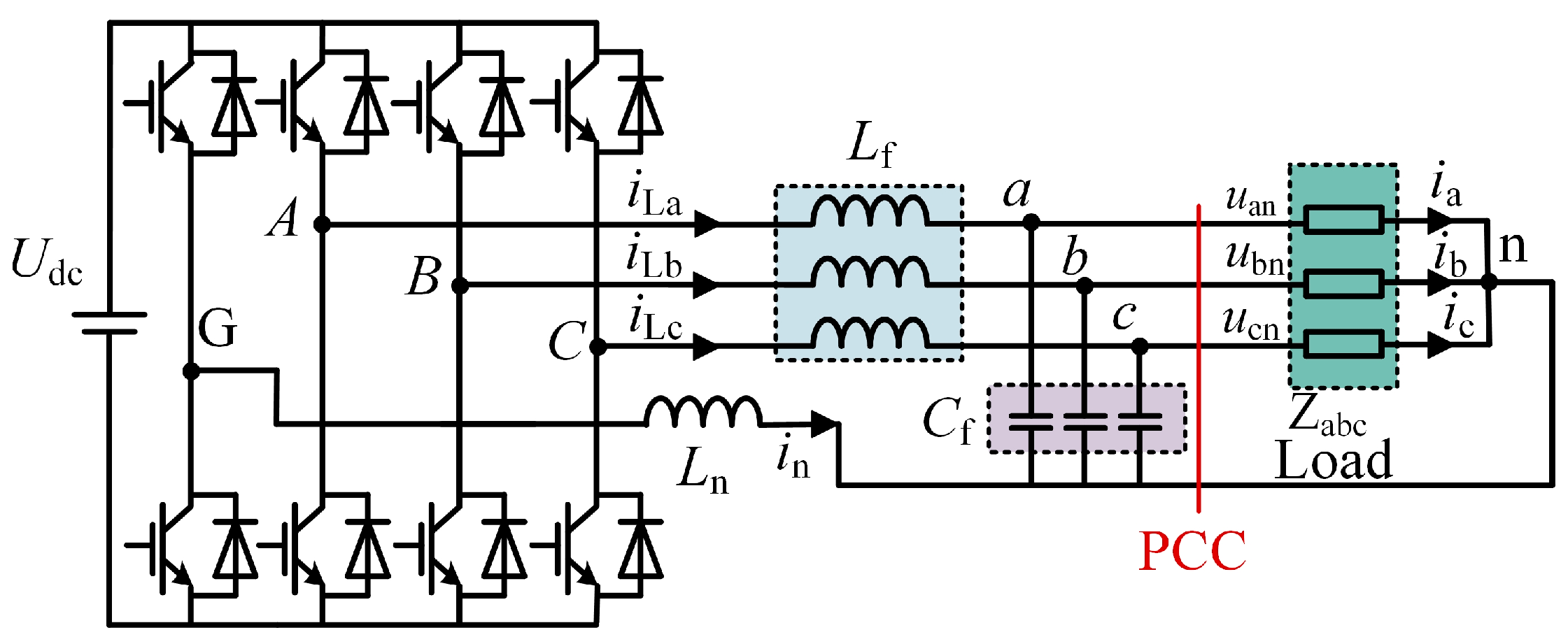
2. Mathematical Model of Four-Leg Inverter

A diagram of an unbalanced load power supply system is shown in Figure 1 [39]. In practical power supply systems, load imbalance is frequently encountered due to single-phase loads or unbalanced three-phase loads. To obtain symmetrical voltages and stable frequency for power supply and pre-synchronization, the DC/AC inverter shown in Figure 1 can be used as a four-leg inverter. It is assumed that the load is linear and time-invariant.
The topology of a three-phase four-leg inverter is shown in Figure 2 [23]. Three legs (a, b, c) of the inverter are linked to the three-phase AC loads via an LC filter. The inductance and capacitance are Lf and Cf, respectively. The fourth leg (G) is linked to the neutral point (n) via an inductor Ln. Udc is the DC voltage source, which commonly comes from energy storage or distributed generation. Constraints on the DC side of the inverter are not considered. Thus, Udc is considered as a constant value in this paper.
Since the switching frequency is much higher than the fundamental frequency, the average model of the four-leg inverter can be represented as shown in Figure 3 [23]. The averaged voltages, uAG, uBG, and uCG, are expressed as follows:
u A G u B G u C G = u A u G u B u G u C u G = U d c d a d g d b d g d c d g
where uA, uB, uC, and uG are the voltages relative to the negative terminal on the DC side. da, db, dc, and dg, denote the duty cycles of each upper arm switch.
Based on Kirchhoff’s law and Figure 3, the relationships of voltages and currents can be expressed as follows:
u AG u BG u CG = L f d d t i La i Lb i Lc + u an u bn u cn L n d d t i n i n i n
i La + i Lb + i Lc + i n = 0
i La i Lb i Lc = C f d d t u an u bn u cn + i a i b i c
where, uAG, uBG, and uCG are arm voltages relative to the fourth leg (G). iLa, iLb, and iLc represent the filter inductor current. ia, ib, and ic denote load currents. uan, ubn, and ucn denote the load voltages.
According to Equations (2)–(4), the equation can be rewritten as follows:
d d t i La i Lb i Lc = H 1 u AG u an u BG u bn u CG u cn
d d t u an u bn u cn = 1 C f i La i a i La i b i La i c
where
H = L f + L n L n L n L n L f + L n L n L n L n L f + L n
According to Equations (5) and (7), it is clear that there is coupling in the three phases due to Ln. In order to eliminate the coupling, Clark transformation has been used to implement the transformation from abc to αβγ. The transformation matrix used can be defined as follows:
T = 2 3 1 1 / 2 1 / 2 0 3 / 2 3 / 2 1 / 2 1 / 2 1 / 2
Multiply both sides of Equation (5) by Equation (8) [34]. The following equation can be obtained:
d d t i L α i L β i L γ = 1 / L f 0 0 0 1 / L f 0 0 0 1 / L f + 3 L n u α G u α n u β G u β n u γ G u γ n
Similarly, the transformation of Equation (6) results in the following:
d d t u α n u β n u γ n = 1 C f i L α i α i L β i β i L γ i γ
where [ uαG, uβG, uγG]T and [ uαn, uβn, uγn]T are the arm voltages relative to the fourth leg (G) and voltages of loads in the αβγ reference frame. [iLα, iLβ, iLγ]T and [ iα, iβ, iγ]T denote the currents of inductor and load in the αβγ reference frame.
Based on Equations (9) and (10), the equivalent mathematical models of the α, β, and γ components are symmetrical. It is evident that there is no coupling among the α, β, and γ components. Therefore, the controllers of the α, β, and γ components can be designed separately.

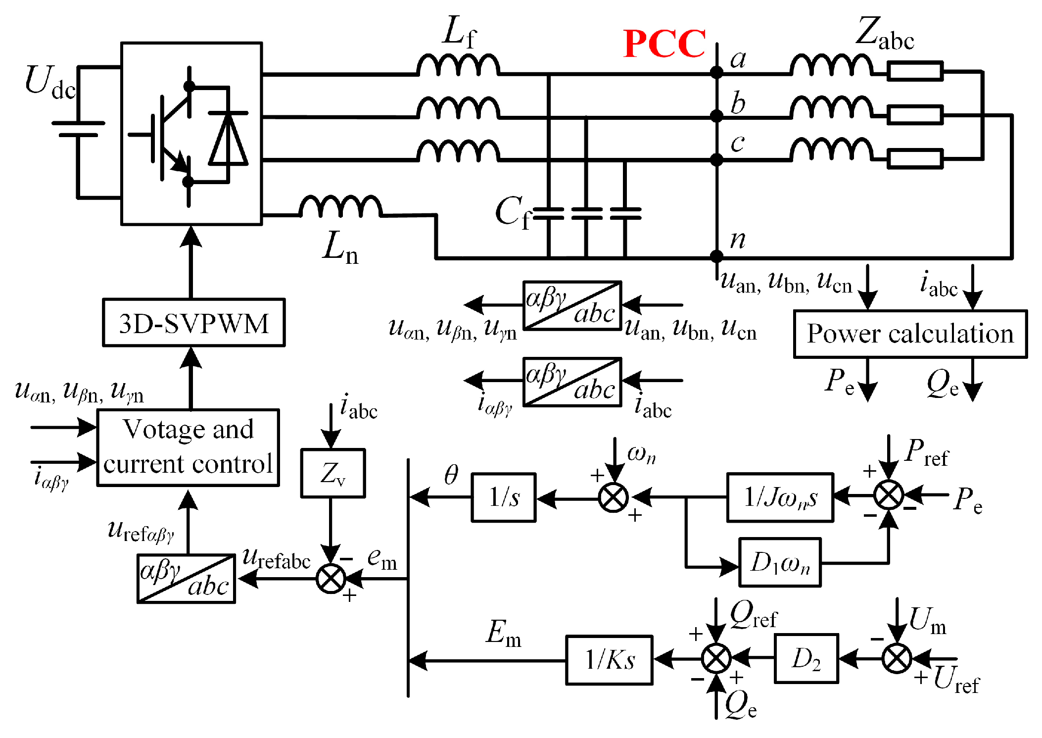
3. Improved VSG Control Strategy for a Four-Leg Inverter

3.1. Problems in the Existing Control Strategy

Figure 4 illustrates the diagram of the existing control strategy for a four-leg inverter under load variation. According to [40,41], the existing power control of VSG can be described as follows:
J ω n d ω d t = P ref P e D 1 ω n ( ω ω n )
E m = 1 K s ( Q ref Q e + D 2 ( U ref U m ) )
where Pref and Pe denote the reference active power and the calculated active power at point of common coupling (PCC) points, respectively. Similarly, Qref and Qe are reactive power. J and D1 represent the virtual inertia constant and damping coefficient, respectively. D2 and K represent the voltage regulation coefficient and integral regulation coefficient, respectively. ωn denotes the reference angular frequency. ω is the angular frequency of VSG output. Em denotes the magnitude of internal electric potential of VSG, and Uref and Um are the reference and measurement of voltage magnitude, respectively.
In general, virtual impedance is introduced to enhance the performance of VSG. The reference of VSG output voltage can be obtained as follows [38,42]:
u refabc = e m i abc Z v
The problems of the existing control strategy are also presented in Figure 5. When the loads are balanced, the voltages are balanced, and the frequency has no ripple. However, the voltage asymmetry and frequency ripples appear due to load asymmetry, which is challenging for power supply and pre-synchronization. Thus, the existing control strategy need to be improved to suppress the voltage unbalance and frequency ripples.

3.2. Improved VSG Control Strategy

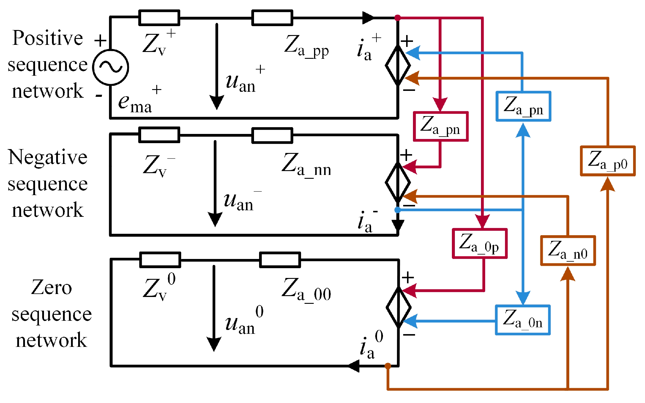
3.2.1. Improved Virtual Impedance Method

Assuming that the load is linear, according to Figure 2, the following equation can be obtained:
u an u bn u cn = Z a 0 0 0 Z b 0 0 0 Z c i a i b i c
where uan, ubn, and ucn are load voltage, and ia, ib, and ic represent load current. Za, Zb, and Zc denote the impedances of the load.
Take phase A as a reference. Based on the symmetrical component method [43], Equation (14) can be transformed into the following Equation (15):
u an + u an u an 0 = M Z a 0 0 0 Z b 0 0 0 Z c M 1 i a + i a i a 0
where
M = 1 3 1 a a 2 1 a 2 a 1 1 1
where a = ej120°, and a2 = e j240°. u an + , u an , u an 0 are the sequence components of uan, ubn, and ucn. i a + , i a and i a 0 represent the sequence components of ia, ib, ic.
Equation (15) can be rewritten as follows:
u an + u an u an 0 = Z a _ pp Z a _ pn Z a _ p 0 Z a _ np Z a _ nn Z a _ n 0 Z a _ 0 p Z a _ 0 n Z a _ 00 i a + i a i a 0
where Za_pp, Za_nn, and Za_00 are the sequence components of load impedances, respectively. Za_ij is the coupling impedance between sequence i and sequence j.
Similarly, Equation (13) can be transformed into Equation (18).
e ma + u an + e ma u an e ma 0 u an 0 = Z v + 0 0 0 Z v 0 0 0 Z v 0 i a + i a i a 0
where e ma + , e ma , and e ma 0 are the sequence components of em. Z v + , Z v , and Z v 0 are the sequence components of Zv.
Basically, e ma and e ma 0 are zero. According to (17) and (18), an equivalent sequential network model of VSG with an unbalanced load is represented in Figure 6. The impedances are coupled due to the unbalanced loads. Thus, u an + , u an , and u an 0 and i a + , i a , and i a 0 are coupled. The coupling relationship is represented by the controllable voltage source.
According to Figure 6, the positive sequence current and coupling impedances result in the formation of negative and zero sequence controllable voltage sources. Then, negative sequence and zero sequence currents are generated. u an and u an 0 ( u an = − i a Z v , u an 0 = − i a 0 Z v 0 ) are produced, which results in three-phase voltage unbalance at PCC points.
The improved virtual impedance is proposed based on Equation (18) and Figure 6. If Z v and Z v 0 are zero, the negative sequence voltage and zero sequence voltage of the loads at PCC points are eliminated. Therefore, the improved virtual impedance can be utilized to mitigate voltage imbalance.

3.2.2. Power Calculation Method

When the load voltages are balanced, uan, ubn, and ucn can be expressed as follows:
u an u bn u cn = 2 U cos ( ω t ) 2 U cos ( ω t 2 π / 3 ) 2 U cos ( ω t + 2 π / 3 )
where U is the RMS value of the load voltage.
Due to the load imbalance, the currents can be expressed as follows:
i a + i b + i c + = 2 I + cos ( ω t + φ i + ) 2 I + cos ( ω t + φ i + 2 π / 3 ) 2 I + cos ( ω t + φ i + + 2 π / 3 ) i a i b i c = 2 I cos ( ω t + φ i ) 2 I cos ( ω t + φ i + 2 π / 3 ) 2 I cos ( ω t + φ i 2 π / 3 ) i a 0 = i b 0 = i c 0 = 2 I 0 cos ( ω t + φ i 0 )
where I+, I, and I0 are the RMS value of i a + , i a , and i a 0 . φ i + , φ i , and φ i 0 are the initial phase angles of the sequence currents.
Based on [44], the equation of active power can be rewritten as follows:
p = u an i a + u bn i b + u cn i c
According to Equations (19)–(21), the following equation can be obtained:
p = p ¯ + p ˜ = 3 U I + cos φ i + + 3 U I cos ( 2 ω t + φ i )
where p ¯ represents average power, and p ˜ is the oscillating power, which is the main cause of the power ripple.
According to Laplace transform, Equation (11) can be rewritten as follows:
ω ( s ) = ( P ref P e ( s ) ) / ω n + D 1 ω n J s + D 1
Based on Equations (22) and (23), the angular frequency in the frequency domain can be expressed as follows:
ω ( j 0 ) = ( P ref P e ) / ω n + D 1 ω n D 1
ω ( j 2 ω ) = ( 0 P e ( j 2 ω ) ) / ω n J j 2 ω + D 1
According to Equations (24) and (25), the angular frequency includes both a DC component and a double-frequency component. If Pref is equal to Pe at steady state, the DC component of ω is ωn. The oscillating active power can be represented by Pmcosφi + jPmsinφi, where Pm is the RMS of the oscillating power. The double-frequency gain of the angular frequency can be expressed as follows:
ω ( j 2 ω ) = P m 100 π D 1 2 + 40000 π 2 J 2
When the oscillating active power increases, the ripple of the voltage frequency will exceed the allowable range. This will endanger the normal operation of the system. It can also be proved that reactive power ripple has an impact on VSG control through similar methods. However, it is not covered in the article.
According to Equations (22)–(26), the power calculation method is presented. If VSG outputs are balanced voltages, there will be active power ripples. The oscillating active power will cause a frequency ripple. Therefore, the average active power is used as feedback for the improved VSG control strategy.

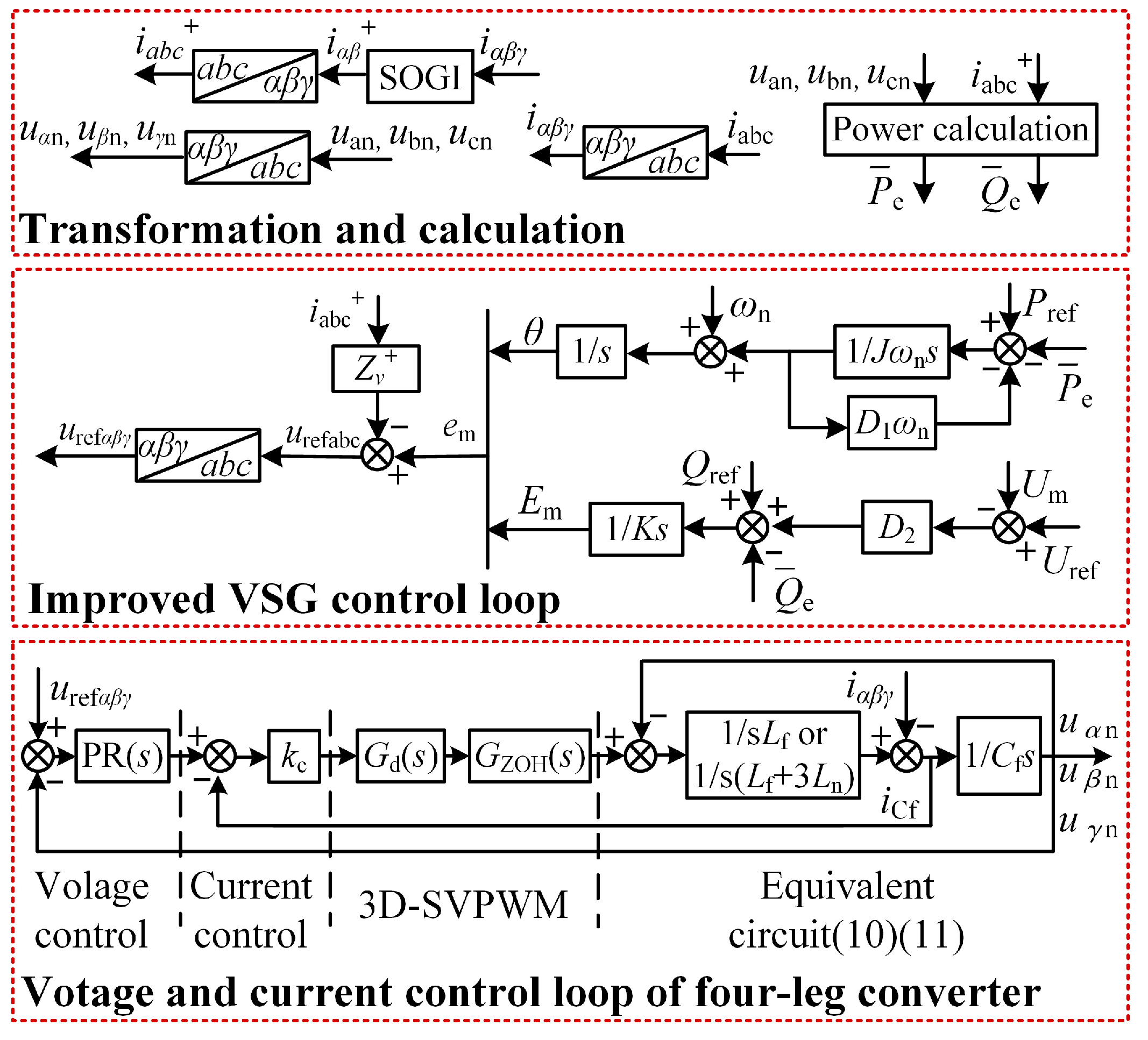
3.2.3. Control Block Diagram

To address the voltage unbalance and voltage frequency ripple caused by unbalanced loads, an improved VSG control strategy is put forward. Figure 7 shows the improved VSG control block diagram.
Based on the derivation mathematical model of four-leg inverter in Section 2, Equations (9) and (10) can be obtained. It is evident that there is no coupling among the α, β, and γ components. What is more, the mathematical model of the four-leg inverter in the αβγ reference frame is similar to that of three phase voltage source converters with LC [45]. Therefore, the voltage and current control loop of four-leg inverter in Figure 7 can be derived.
Figure 7 depicts the control loops of the four-leg inverter in the αβγ reference frame. The current control loop is a proportional (P) controller, which takes the capacitive current as feedback. iCf denotes the capacitance current. A proportional-resonant (PR) controller is used in voltage control loop to achieve accurate voltage reference tracking.
Gd(s) represent the control delay of the digital system. GZOH(s) denote a zero-order holder, which is the characteristic of the modulation. Gd(s) and GZOH(s) can be expressed as follows:
G d ( s ) = e s T s G ZOH ( s ) = 1 e s T s s
where Ts is the sampling period.
According to Section 3.2.1, it can be concluded that if the virtual impedances of negative and zero sequence are zero, the negative sequence voltage and zero sequence voltage of the loads at PCC points are eliminated. Therefore, an improved virtual impedance method is proposed, and the positive sequence of virtual impedance is integrated into the control. This can be expressed as follows:
u refabc = e m i abc Z v +
In addition, Section 3.2.2 analyzes the influence of power calculation in VSG control under an unbalanced load. It can be concluded that there is oscillating active power under an unbalanced load. The oscillating active power will cause a frequency ripple. Therefore, the average power is used as feedback for the improved VSG control strategy. Therefore, the following equation can be obtained:
J ω n d ω / d t = P ref P ¯ e D 1 ω n ( ω ω n ) E m = ( Q ref Q ¯ e + D 2 ( U ref U m ) ) / K s
where P ¯ e and Q ¯ e denote the average active and reactive power at PCC points, respectively. Zv+ is the positive sequence virtual impedance.
In addition, a second order generalized integrator (SOGI) is presented to separate the positive and negative component, which can be rewritten as follows:
i α + i β + = 1 2 1 ( j ) j 1 i α i β
where j = ejπ/2.
The feedback of active power can be expressed as follows:
P ¯ e = u an i a + + u bn i b + + u cn i c +
where uan, ubn, and ucn denote the load voltages at PCC points. i a + , i b + , and i c + represent the positive sequence currents flowing through the load.

4. Improved VSG Pre-Synchronization Control Strategy for a Four-Leg Inverter

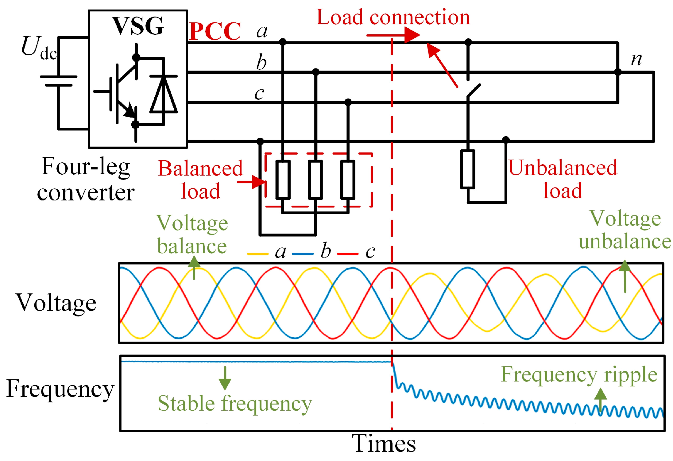
4.1. Analysis of a VSG Control Strategy from Isolated Mode to Grid-Connected Mode under Unbalanced Loads

The four-leg inverter can be used as the connection between microgrid and power grid. It is capable of operating both in isolated mode and in grid-connected mode. In isolated mode, the four-leg inverter employing the VSG control strategy can be considered a voltage source. It can support the voltage and frequency for unbalanced loads, as detailed in Section 3. In grid-connected mode, the active and reactive power references can be accurately tracked. The frequency and voltage output by the inverter are consistent with the power grid. It can provide active and reactive support when the grid voltage and frequency drop.
In Figure 8, the inverter is linked to the power grid by the line impedance ZLine. The VSG control strategy is employed in isolated mode. Thus, the voltage amplitude, frequency and phase output by inverter are different from the grid at the time of mode switching, which will result in a large current rush. If the grid is connected at this time, it will lead to a large impact current, which can easily cause accidents and component damage.
Three key conditions must be met for the inverter to transition from off-grid to grid-connected operation. First, the inverter’s output voltage amplitude must match that of the power grid. Second, the frequency of the voltage is consistent with that of the power grid. Third, the phase of output voltage is equal to the grid. However, it can be seen from Section 3 that the unbalanced voltages and frequency ripple are caused by unbalanced loads. Thus, the impulse current must exist when using traditional VSG control, because the above three conditions cannot be met. The improved VSG control strategy proposed in Section 3 makes it possible to have an inverter with seamless transfer. The improved VSG-based pre-synchronization control strategy for four-leg inverters requires further study.

4.2. Design of Improved VSG-Based Pre-Synchronization Control Strategy

Based on the pre-synchronization control strategy [46], the VSG-based pre-synchronization control strategy for a four-leg inverter is put forward in Figure 9. The phase pre-synchronization is designed according to the PLL and Park transformation. The amplitude and phase angle differences between the output voltages of inverter and the grid voltage are the result of the DC component. Therefore, the PI controller is designed to diminish the amplitude and phase angle difference between the output voltages of inverter and the grid voltage.

4.2.1. Phase Pre-Synchronization

The phase of power grid θg can be obtained by using a phase-locked loop (PLL). uU, uV, and uW represent the voltages of the power grid. The schematic diagram of the PLL is displayed in Figure 10. According to Equation (8), the voltages of the power grid uα, uβ can be obtained by Clark transformation. The voltages of power grid ud, uq can be calculated by Park transformation. The transformation matrix is expressed as follows:
F = cos θ g sin θ g 0 sin θ g cos θ g 0 0 0 1
where θg is the phase of power grid.
The proportional-integral (PI) controller is applied to make the uq calculated by Park transformation equal to zero. The output angular frequency by the PI controller is added to ωn to obtain the angular frequency of the grid. The output angular frequency from the PI controller is added to ωn to produce the angular frequency of grid. The voltage phase of a power grid can be obtained by the integral of the angular frequency.
The voltages uan, ubn, and ucn that are output by the four-leg inverter are transformed by Park transformation to obtain inverter voltage uqn. The reference angle in Park transformation is the power grid angle θg. The uqn is zero only when the phase of the grid aligns with the phase of the voltage output of the inverter. Therefore, the PI controller can be used to set uqn to zero. The compensation of angular frequency Δω output by the PI controller is used to adjust the angular frequency of the four-leg inverter, with the goal of aligning the voltage frequency and phase with those of the power grid.

4.2.2. Amplitude Pre-Synchronization

Root mean square (RMS) is used to obtain the voltages U and Ug. U and Ug are the RMS voltages of the four-leg inverter and power grid, respectively. The PI controller is proposed to ensure that the voltage U output by the inverters matches the reference voltages of power grid Ug. The voltage compensation output by the PI controller is added to the internal electric potential of VSG, ensuring that the voltage output by the inverter matches the power grid voltage.

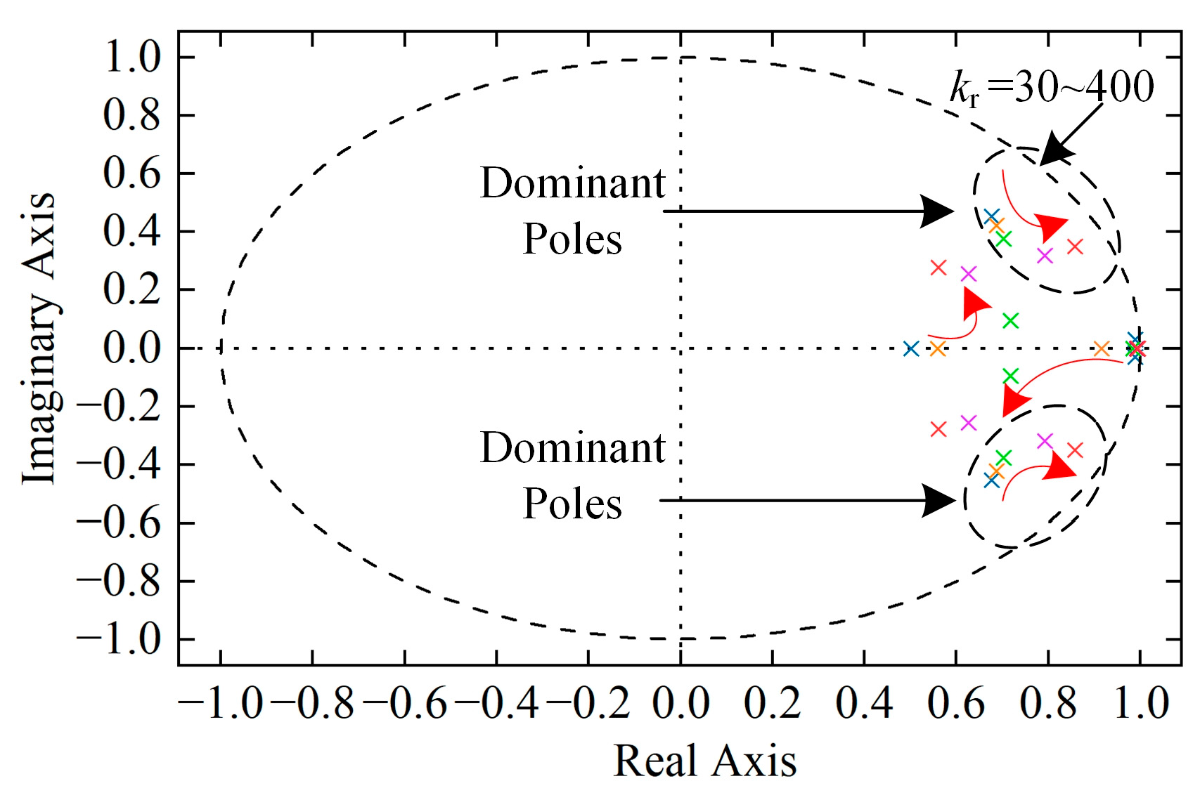
5. Optimized Parameters Design Method

To enhance the dynamic performance of the voltage and current control loops, it is crucial to carefully design the controller parameters. According to [47,48], it can be known that the pole mode diagram is an important method for control analyses. However, at present, the Bode diagram and transfer function are commonly used to design control parameters. Until now, there are few papers using use pole to design control parameters. An optimized design method for control parameters is presented according to the pole map.
Considering that the controllers in the actual system are mostly discrete, the control shown in Figure 6 is designed in the z domain. Based on Equations (9) and (10), designing the controller in the αβγ reference frame yields equivalent results. Consequently, the controller is designed in the α axis. The main circuit parameters of the prototype are listed in Table 2.

5.1. Parameters Design for Current Control Loop

The dynamic performance is influenced by both the voltage and current control loops. The design of the current control loop can be performed independently from that of the voltage control loop. Pole mapping has been used to obtain the optimal parameter. The closer the dominant poles are to the origin of the unit circle, the quicker the dynamic response of the current control loop. From Figure 7, the open-loop and closed-loop transfer functions of the current control loop in z domain can be presented as follows:
G c o ( z ) = k c sin ( ω r T s ) ( z 1 ) L f ω r z ( z 2 2 z cos ( ω r T s ) + 1 )
G cc ( z ) = G co ( z ) 1 + G co ( z )
where Ts is the sampling period. kc denotes the proportional parameter. ωr denotes 1 / L f C f .
If the inductance and capacitance remain constant, the dynamic performance of the current control loop depends on the variable parameter kc. Figure 11 shows the pole map of the closed-loop transfer function as kc varies. As kc increases from 1 to 16, a pair of conjugate poles initially approaches the original point before moving away from it. When kc is 6.7, the dominant poles are closest to the original point, as determined by the traversal comparison. The accurate kc, closest to the original point, can be calculated by a complex process. However, it is not meaningful. The parameter, obtained by traversal, has a better dynamic response.
For the stability analyses, the gain margin (GM) and phase margin (PM) are used to check the stability of the system, which can be obtained by Bode diagram or the open-loop transfer function. According to [49], it can be known that the generally accepted method of determining the stability margins is GM > 3 dB and PM > 30°.
If kc can satisfy the requirement of stability margins, it is the optimized kc_O. If the stability margins cannot be met, kc needs to be increased or decreased to obtain kc_O. After calculation, when kc is 6.7, GM and PM are 8.18 dB and 37.6°, respectively, which meets the requirement of stability margins. Therefore, kc_O is the optimized parameter on the α axis.

5.2. Parameters Design for Voltage Control Loop

The parameter design process of voltage control loop is similar to that of current control loop. The voltage controller used in this paper is a proportional-resonant (PR) controller, and the transfer functions of the voltage controller in the s domain can be expressed as follows:
G PR ( s ) = k v + k r s s 2 + ω n 2
where kv represent the proportional parameters. kr is the resonant parameters. ωn is the reference angular frequency.
The pre-warped Tustin z transformation can be represented as follows:
s = ω i tan ω i T s 2   ·   z 1 z + 1
where, ωi is frequency band where the error of the z transformation is reduced. In this paper, ωi is ωn.
According to Equations (34) and (35), the voltage controller in the z domain can be expressed as follows:
G PR ( z ) = k v + k r sin ( ω n T s ) ( z 2 1 ) 2 ω n ( z 2 2 z cos ( ω n T s ) + 1 )
To streamline the voltage control loop design, the P component can be excluded. The R controller is used to enhance system performance. According to Figure 7, the open-loop and closed-loop transfer functions in z domain can be expressed as follows:
G vo ( z ) = G R ( z ) × k c ( 1 cos ( ω r T s ) ) ( z + 1 ) z ( z 2 2 z cos ( ω r T s ) + 1 ) + k c sin ( ω r T s ) ( z 1 ) / ( L f ω r )
G cc ( z ) = G vo ( z ) 1 + G vo ( z )
Since only one parameter of the PR controller needs to be designed, the pole map of the voltage control loop can also be used to design the optimized parameter.
Figure 12 shows the pole map of the voltage control loop as kr varies. The pole map of the voltage control loop varying with kr is shown in Figure 12. As kr increases, a pair of conjugate poles first approaches the original point and then moves away. When kr is 190, the dominant poles are closest to the original point, as determined by traversal comparison.
If kr can satisfy the requirement of stability margins, it is the optimized kr_O. The generally accepted method of determining the stability margins is GM > 3 dB and PM > 30°. If the stability margins cannot be met, kr needs to be increased or decreased to obtain kr_O. When kc is 190, GM and PM are 8.47 dB and 62.5°, which meet the requirement of the stability margins. Thus, kr_O is the optimized parameter on the α axis.
Based on Equations (9) and (10), the voltage and current control loops on the α axis are the same as that on the β axis. However, due to the neutral inductance, the equivalent filter inductance is Lf+3Ln on the γ axis. The above calculation method is used to obtain the optimized parameters. When kc_Oγ is 13.8, GM and PM are 10.7 dB and 52.9°, respectively. When kr_Oγ is designed as 40, GM and PM are calculated as 13.9 dB and 67.5°, respectively. The controller parameters meet the requirements of the stability margins.

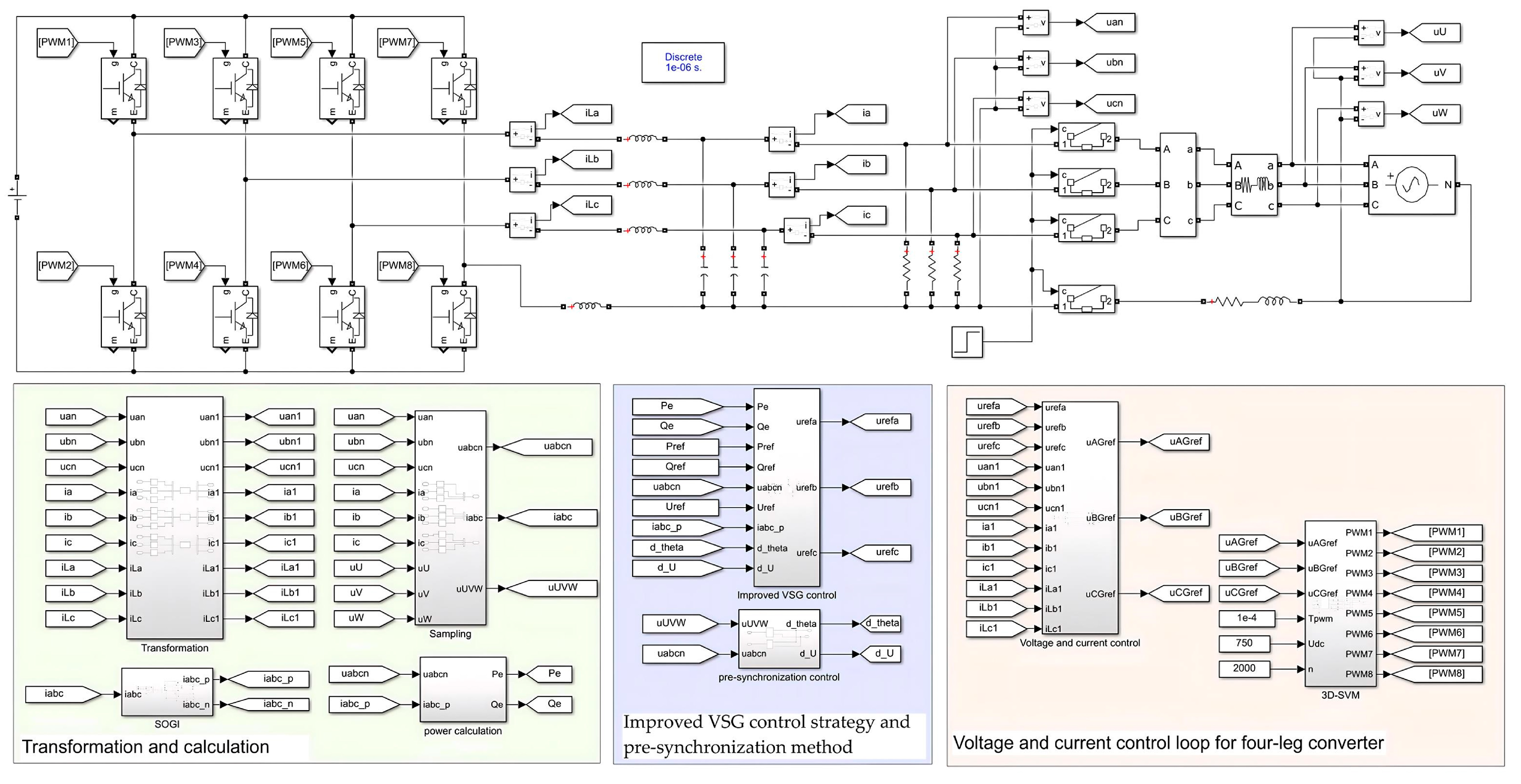
6. Simulation Verifications

In this section, the simulation is carried out in MATLAB/Simulink. The simulation model of the main circuit and proposed control strategy is shown in Figure 13 [39]. The proposed improved VSG-based control strategy and pre-synchronization method of a four-leg inverter can be verified by the simulation results. The parameters of the simulation are shown in Table 3.
The three-phase loads are set to 8 kW, 4 kW, and 1 kW for phases a, b, and c, respectively. The simulation results with different inverter and VSG controls are shown in Figure 14.
In Figure 14a, the neutral point is not grounded. When using traditional VSG for a conventional inverter, the phase voltages are seriously asymmetrical. The total harmonic distortion (THD) of output voltages is 2.6%. Figure 14b shows the simulation results of traditional VSG for a four-leg inverter. Compared with Figure 14a, the voltages are slightly asymmetrical. In this case, The THD of output voltages is 0.99%. However, in Figure 14c, with improved VSG for four-leg converter, the output voltages in PCC points are almost symmetrical. The THD is reduced to 0.85%. The proposed improved control strategy can be verified by the traditional converter and control method.
In Figure 15, the simulation results of the power grid voltage and four-leg converter voltage under pre-synchronization control are shown. At this time, the three-phase loads of a, b, and c are also 8 kW, 4 kW, and 1 kW, respectively. The voltages of phase A are shown in Figure 15. As the pre-synchronization control strategy works, the phase and amplitude of power grid voltage are rapidly consistent with the four-leg converter voltage. The difference in amplitude and phase angle between the output voltages of the converter and the grid voltage has decreased.

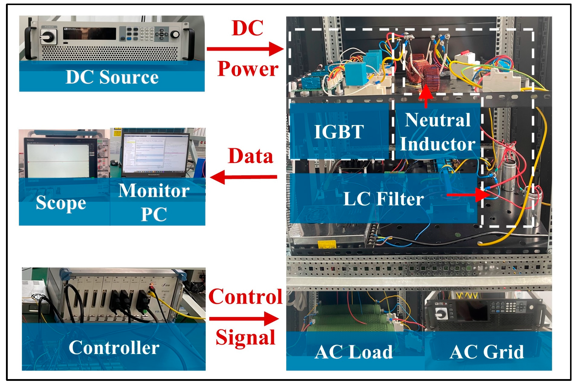
7. Experimental Verifications

A down-scaled prototype of a four-leg inverter is built for experimental verification. The photograph is shown in Figure 16. The primary side of the experimental setup contains a DC source, AC grid, and the main circuit. The DC source is an ITECH 6018C-1500-40, which provides DC power for the entire system. The AC grid is a grid simulator IT7930-350-180, which can output changed AC voltage. The verifications of the improved VSG pre-synchronization control strategy can be carried out conveniently through it. The main circuit includes an IGBT-based four-leg inverter, LC filter, and AC load. The secondary side of the experimental setup includes the controller and scope. The controller is a digital signal process (DSP)-integrated board. It is produced by a Chinese manufacturer and is named Yxspace SP6000. The control chip of it is a DSP TMS320C6747. The oscilloscope is Tektronix-MOS54. It has four sampling channels, and the sampling rate of it is 6.25 GS/s, which is helpful for observing the actual voltage and current waveforms.
To make the hardware connection clearer, a single-line diagram of the experimental setup is shown in Figure 17. The single-line diagram of the experimental setup is divided into two parts. The first part represents the main power circuit. The other part is the control circuit and sampling circuit. The main power circuit includes a DC source, IGBT-based four-leg inverter, LC filter, AC load, and AC grid. The connections between them are shown in Figure 17. Two types of Hall current sensors are used in the sampling circuit to obtain voltage and current signals. The voltage sensor is a CHV-25P, which can measure AC voltage and DC voltage in isolation. The current sensor is an LA-50P, which also can be used to obtain AC or DC current signals. The control circuit is a digital signal process (DSP)-integrated board, through which the output PWM signal and input sampling signal can be obtained. The control chip of it is a DSP TMS320C6747.
Table 4 shows the parameters of the main circuit. In the experimental verification, the virtual inertia J is set to 0.5, the damping coefficient D1 is 30, and the virtual impedance Zv is 3 mH. The voltage regulation coefficient D2 is 321. The controller parameters used in the experiments are presented in Table 4, which are designed by the conventional and proposed method.

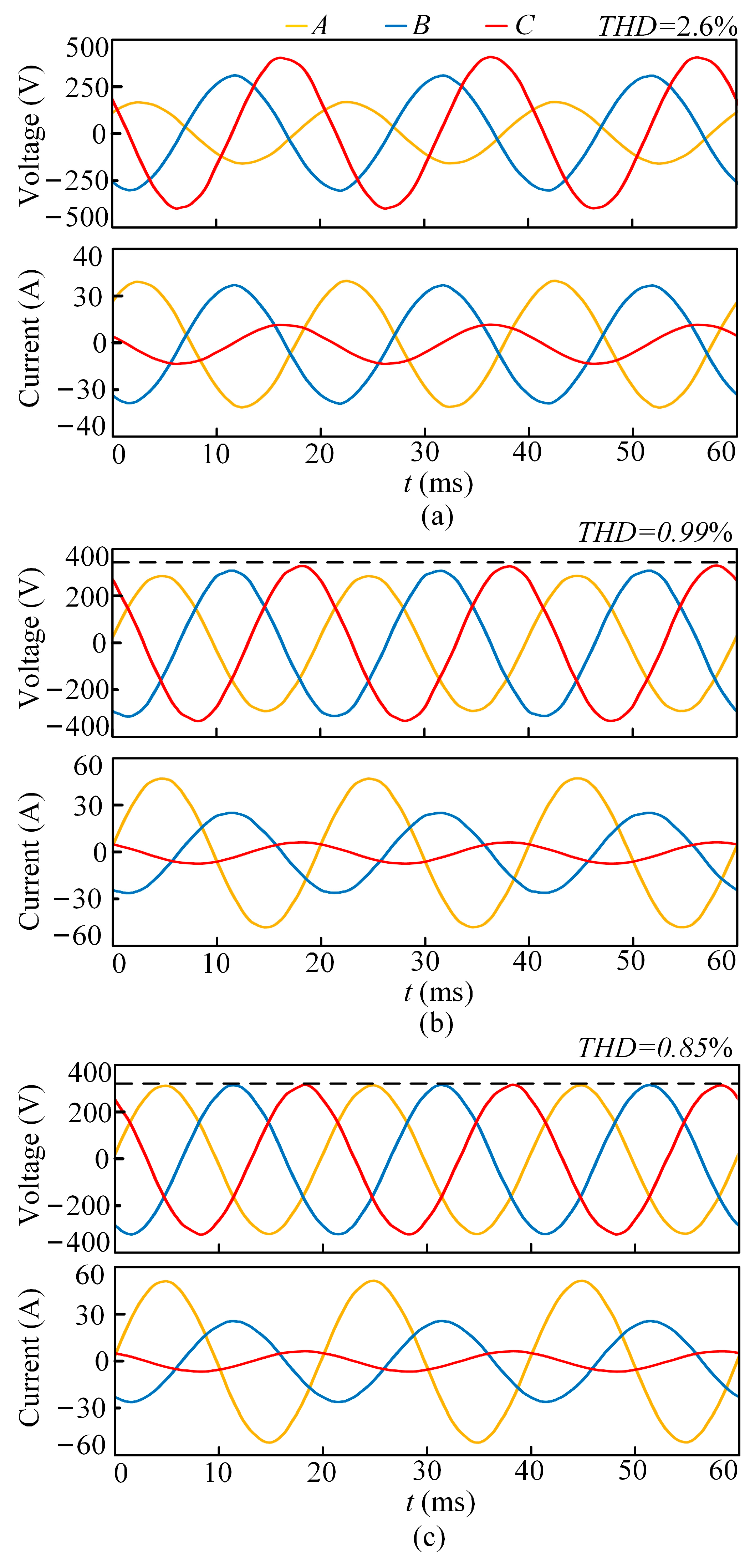
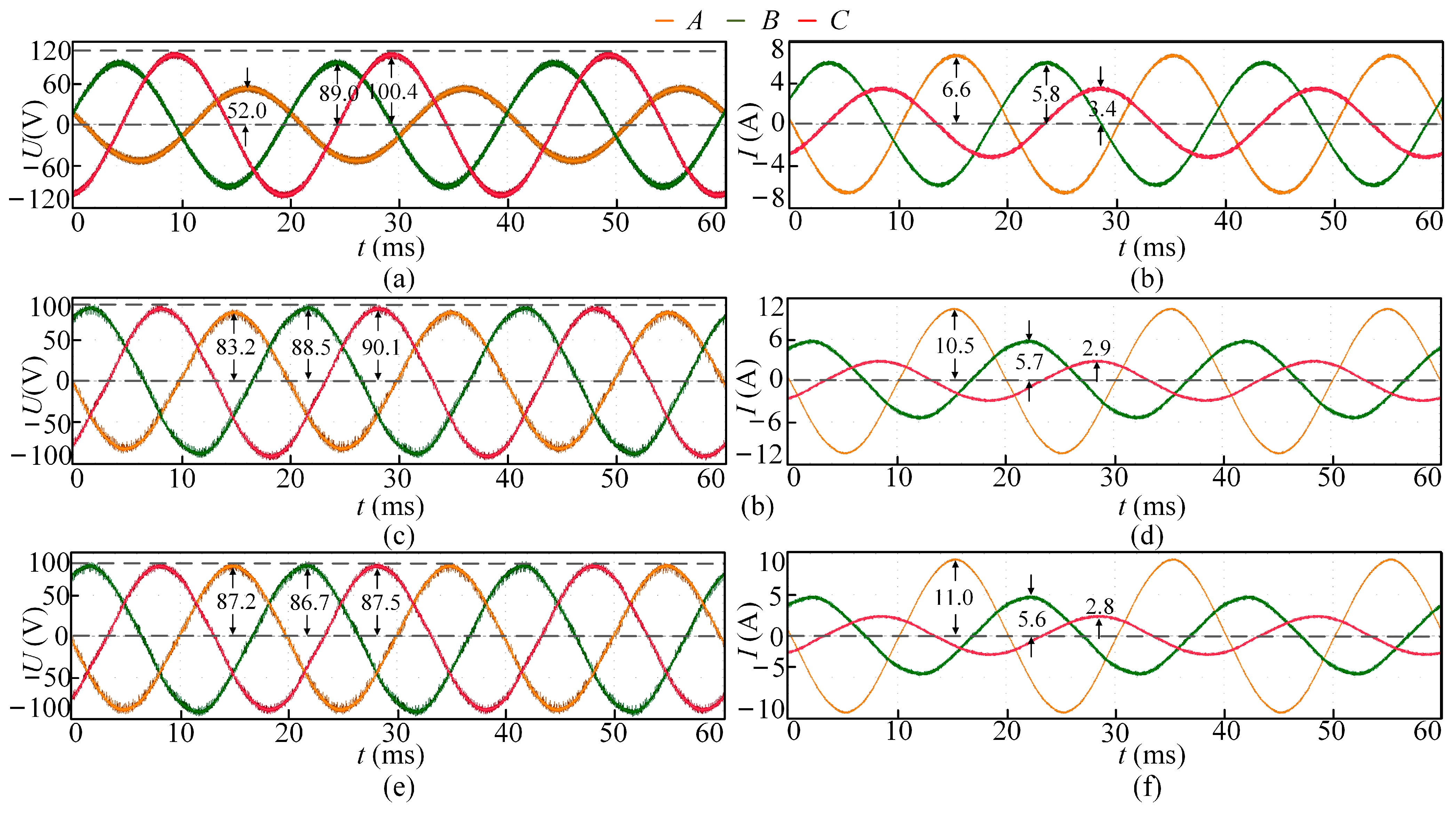
7.1. Verifications of Improved VSG Control Strategy

The three-phase loads of a, b, and c are set as 7.5 Ω, 15 Ω, and 30 Ω, respectively. The optimized parameters shown in Table 4 are also used. The experimental results are shown in Figure 18 and Figure 19. It is worth noting that the conventional converter is usually composed of six switches. There are three phases, and each phase has two switches.
Figure 18a,b present the steady-state waveforms of the traditional VSG applied to a conventional inverter [40]. The neutral point is not grounded. According to the standard equation of the unbalance ratio, the negative sequence unbalance ratio of voltage is 18.2%. Figure 18c,d show the waveforms of a traditional VSG [38] for a four-leg inverter. The negative sequence unbalance ratio of voltage is 2.4%. However, the requirement of negative sequence voltage unbalance is less than 2%. The above two strategies cannot meet the requirement. Figure 18e,f display the waveforms for the improved VSG control strategy applied to the four-leg inverter, with a negative sequence voltage unbalance ratio of 0.26%.
Two strategies are used in the four-leg inverter. When the system is started, the frequency waveforms are shown in Figure 19. Compared with traditional control strategy, it is obvious that the frequency ripple is suppressed by adopting the improved VSG control. In conclusion, the proposed VSG control strategy effectively maintains frequency stability under unbalanced load conditions.
When the system runs at the rated state, the loads are all 10 Ω. The active power of phase A is increased by 180 W. The waveforms are shown in Figure 20. The three-phase voltages remain basically unchanged when the unbalanced load is turned on.

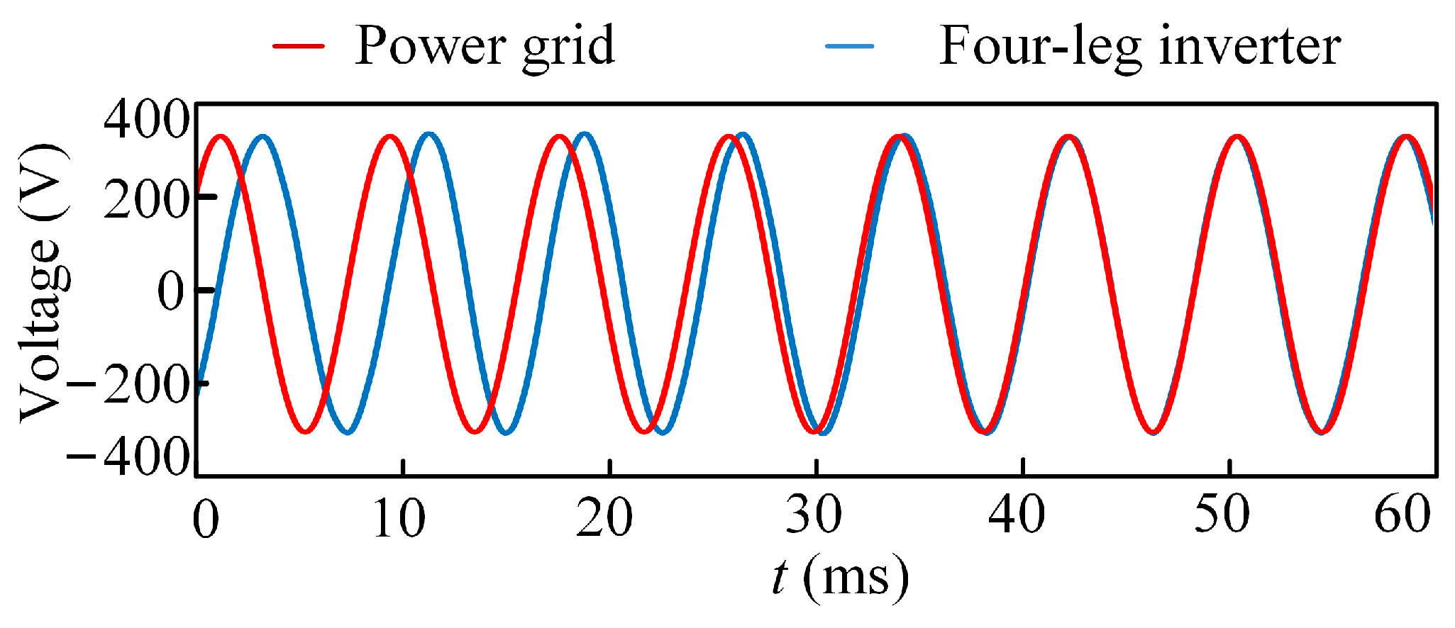
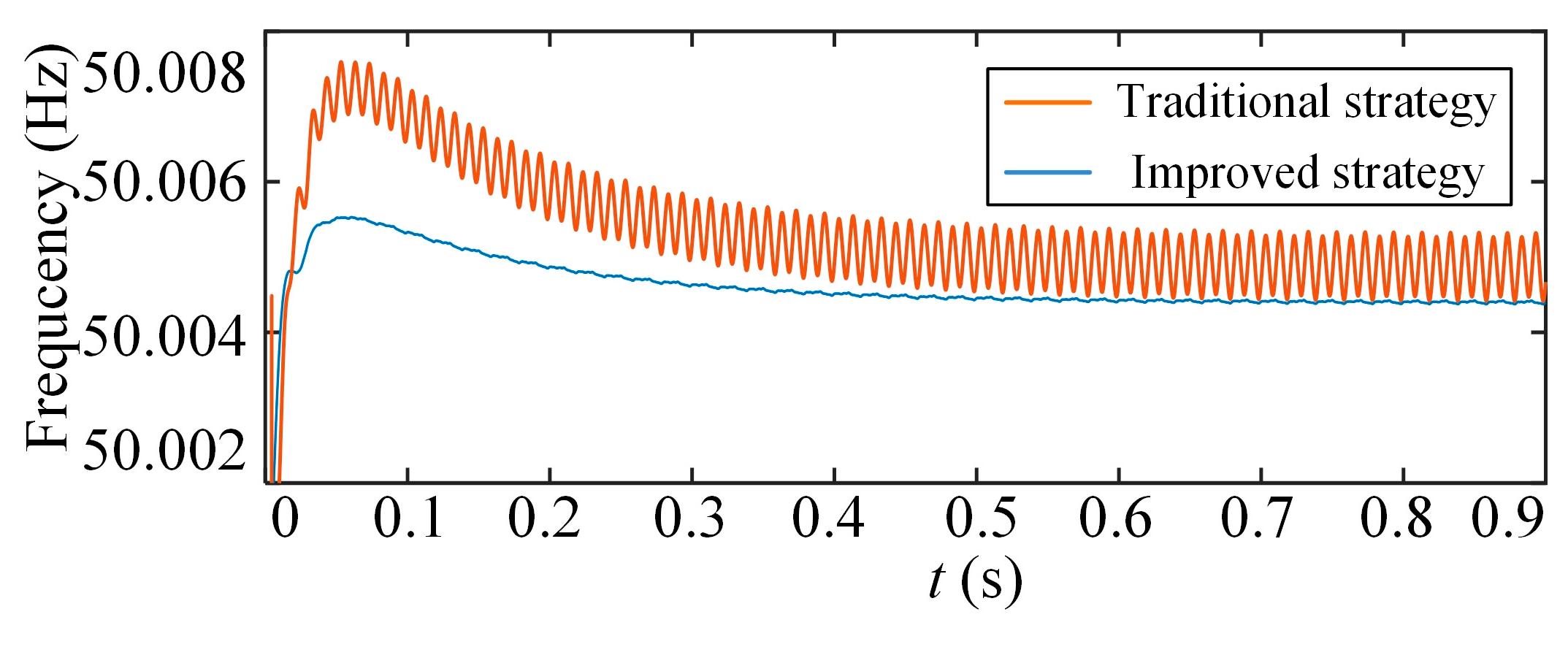
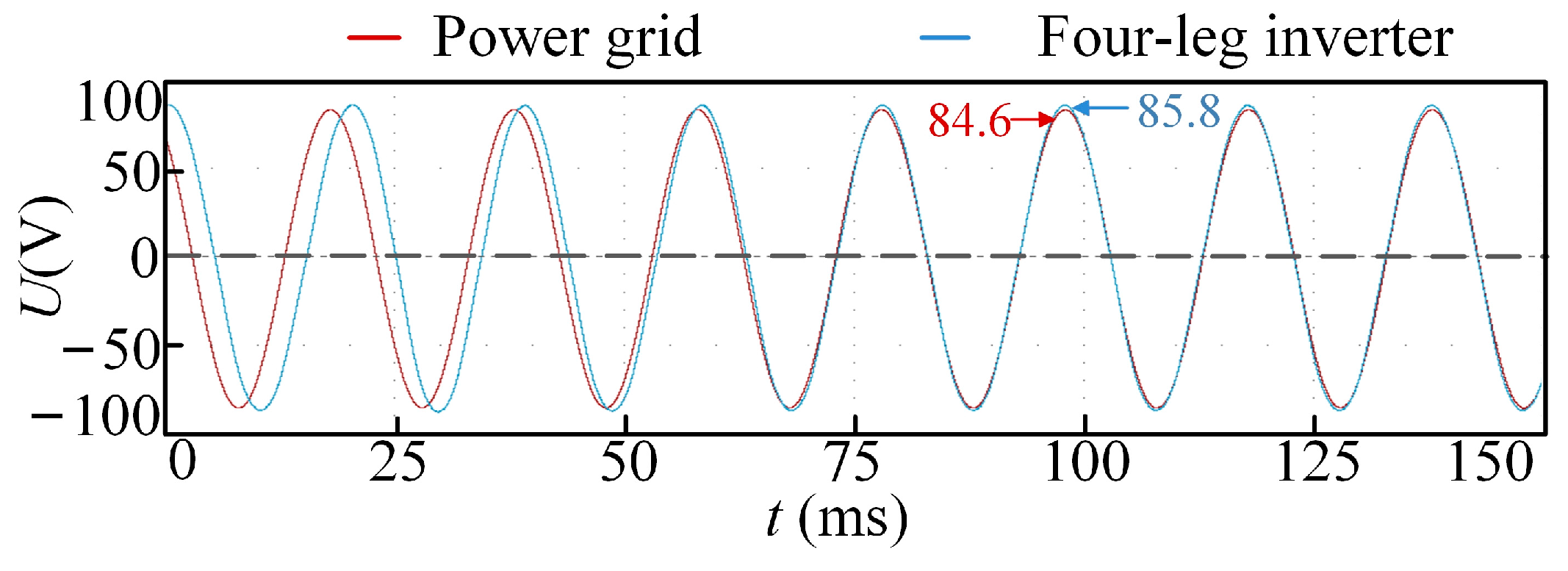
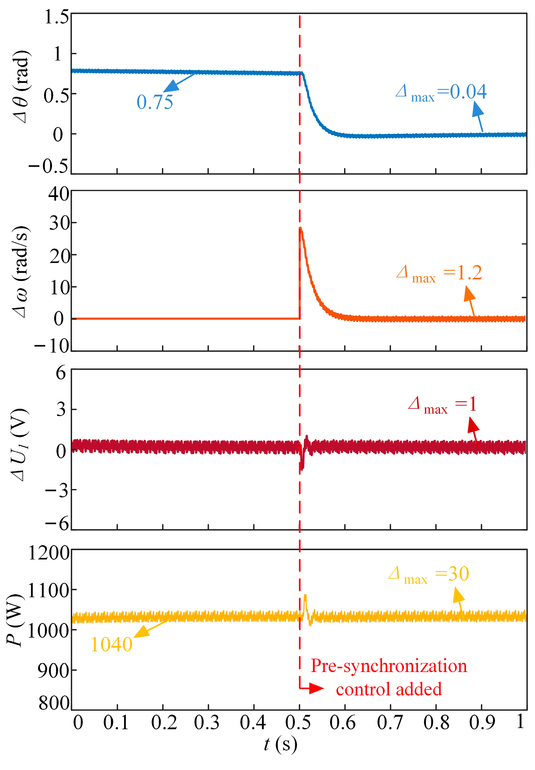
7.2. Verifications of Improved VSG Pre-Synchronization Control Strategy

The phase voltage of the power grid is set to 60 V. Table 2 shows that the rated phase voltage of the four-leg inverter is 60 V. It can be concluded that the symmetrical voltages can be obtained under unbalanced loads, as in Section 7.1. Thus, the loads are all 10 Ω.
The waveforms of the power grid voltage and four-leg converter voltage are shown in Figure 21. The voltages of phase A are used as references. When the pre-synchronization control strategy is added, the phase and amplitude of the power grid voltage are rapidly consistent with four-leg converter voltage. The errors of amplitude are caused by sampling error, device parameter errors, and energy loss.
Figure 22 shows the pre-synchronization process waveforms. Δθ denotes the phase difference between the grid and inverter output voltages, while Δω represents the difference in their angular frequencies. ΔU1 is the difference in RMS. P denotes the active power output of the four-leg inverter. Before 0.5 s, the output voltage and active power basically follow their references. Pre-synchronization control is introduced at 0.5 s, reducing the phase angle difference between the inverter’s output voltages and the grid voltage. Within 0.1 s, the inverter’s output voltage aligns closely with the grid voltage, and the voltage and active power fluctuations remain within acceptable limits.

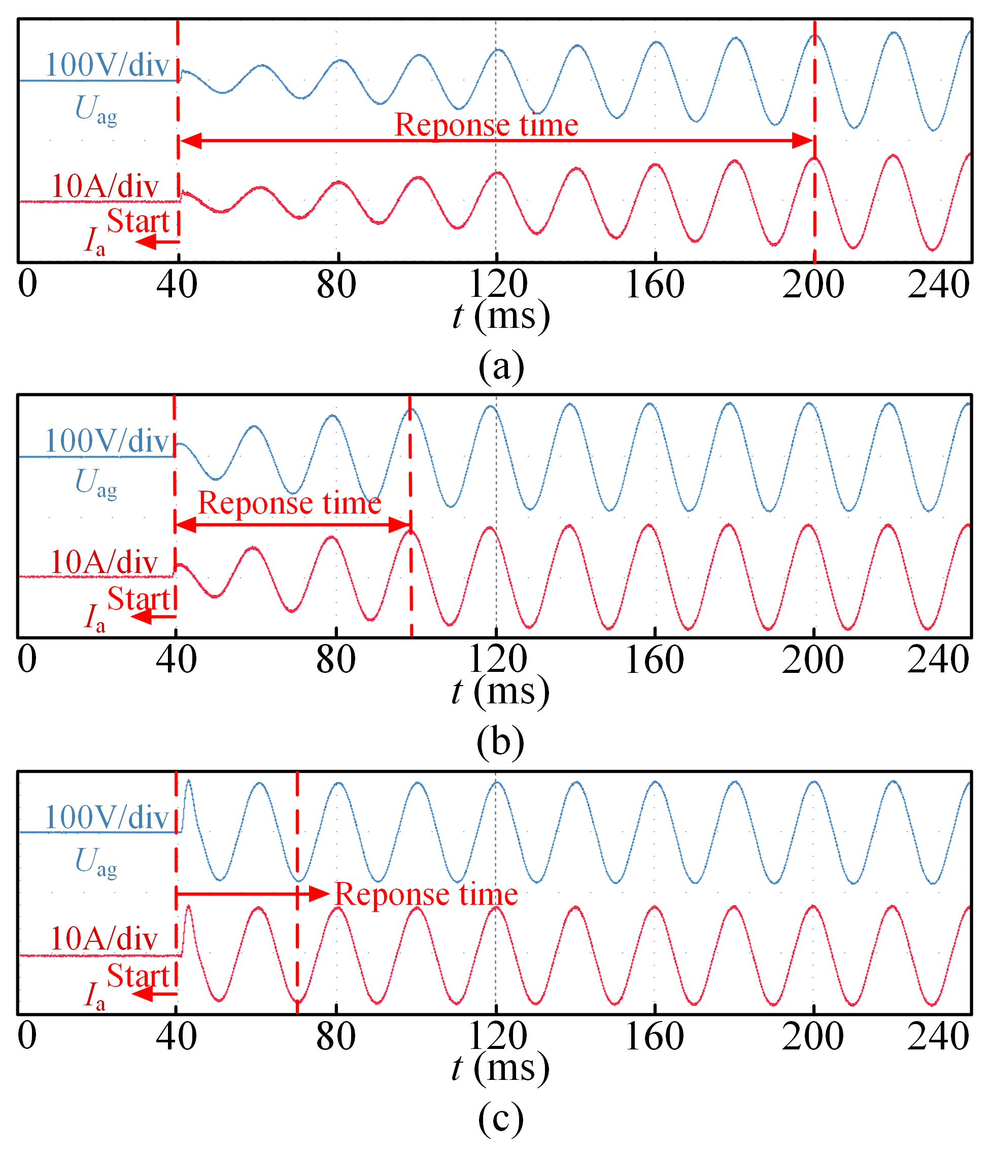
7.3. Verifications of Optimized Parameters Design Method

Table 4 presents three parameters used to validate the proposed design method. The initial voltage is 60 V, and the loads are all 10 Ω. The response time, defined as the duration from initiation to reaching 95% of the steady state, is proposed to evaluate the control system’s dynamic performance. The response time of establishing voltage is compared when the system is started. Take phase A as an example. Figure 22 and Figure 23 display the experimental waveforms.
Figure 23a illustrates the waveforms with parameters I. In this case, the response time is 160 ms. Figure 23b shows the results with parameters II. It can be seen that the response time is 60 ms. The results of the proposed optimized parameters are shown in Figure 23c. The response time is 30 ms, which takes half as long as traditional methods. The effectiveness of the optimized parameters design method is verified.
The active power waveforms are shown in Figure 24. With the proposed optimized parameters, the active power reference is reached first. When parameters I and II are applied in the control loops, the system takes a considerable amount of time to achieve the steady state, significantly impacting its performance.

8. Conclusions

A VSG-based control strategy and pre-synchronization method for a four-leg inverter under an unbalanced load is put forward in this paper. An improved VSG control strategy for a four-leg inverter is put forward. The positive sequence virtual impedance and current are integrated into the control loops for the suppression of voltage asymmetry and frequency ripples. The experiment results show that the voltage unbalance ratio can be reduced by 89%. Furthermore, based on the proposed improved VSG control strategy, a pre-synchronization control strategy is put forward. The pre-synchronization of the voltage amplitude and phase are integrated into the proposed VSG control loop. The results show that the output voltage of the inverter is rapidly synchronized with the power grid voltage.
In addition, an optimized design method for control parameters is presented. The parameters of the voltage control loop and current control loop can be optimized independently. The dynamic performance is improved with satisfying stability margins. From the experimental comparisons, the response time can be shortened by 50%.

Author Contributions

Conceptualization, Z.H. and Z.L.; Methodology, Z.H. and Z.L.; Software, Z.H. and Y.S.; Validation, Z.H., Y.S. and B.S.; Investigation, Z.H. and K.L.; Writing—original draft, Z.H. and G.S.; Writing—review and editing, Z.L., G.S. and K.L.; Supervision, G.S. and K.L.; Funding acquisition, Z.L. and K.L. All authors have read and agreed to the published version of the manuscript.

Funding

This research was funded by the National Natural Science Foundation of China under Grant 52207212 & U2166202; Natural Science Foundation of Shandong Province under Grant ZR2021QE158.

Data Availability Statement

No new data were created or analyzed in this study.

Conflicts of Interest

The authors declare no conflicts of interest.

Nomenclature

Abbreviations
VSGVirtual synchronous generator.
PSOParticle swarm optimization.
PWMPulse width modulation.
MPCModel predictive control.
3D-SVMThree-dimensional space vector modulation.
PI Proportional-integral.
PR Proportional-resonant.
PCCPoint of common coupling.
PProportional.
RMSRoot mean square.
SOGISecond order generalized integrator.
GMGain margin.
PMPhase margin.
PLLPhase-locked loop.
THDTotal harmonic distortion.
Parameters
Lf, LnInductor of LC filter, neutral inductor.
CfCapacitor of LC filter.
UdcVoltage at the DC side of the four-leg inverter.
uA, uB, uC, uGArm voltages relative to the negative terminal on the DC side.
uAG, uBG, uCGArm voltages relative to the fourth leg (G).
da, db, dc, dgDuty cycles of each upper arm switch.
uan, ubn, ucnLoad voltages.
iLa, iLb, iLcCurrents of the filter inductor.
ia, ib, icCurrents of the loads.
inCurrents of the neutral inductor.
uαG, uβG, uγGArm voltages relative to the fourth leg (G) in the αβγ reference frame.
uαn, uβn, uγnLoad voltages in the αβγ reference frame.
iLα, iLβ, iLγFilter currents inductor in the αβγ reference frame.
iα, iβ, iγLoad currents of the in the αβγ reference frame.
Pref, QrefReference active power and reactive power at PCC points.
Pe, QeCalculated active power and reactive power at PCC points.
D1Damping coefficient.
D2Voltage regulation coefficient.
JVirtual inertia constant.
KIntegral regulation coefficient.
ωn, ωReference angular frequency and output angular frequency.
emInternal electric potential of VSG.
EmMagnitude of em.
Uref, UmMagnitude voltages of the output reference and measurement.
ZvVirtual impedance of VSG.
urefabcReference of uan, ubn, ucn.
urefαβγReference of uan, ubn, ucn in the αβγ reference frame.
iabcThree-phase currents of the loads.
I, URMS of ia, ib, ic, RMS of uan, ubn, ucn.
Za, Zb, ZcImpedances of the load.
u an + ,   u an ,   u an 0 Sequence components of uan, ubn, ucn.
i a + ,   i a ,   i a 0 Sequence components of ia, ib, ic.
Za_pp, Za_nn, Za_00Sequence components of Za, Zb, Zc.
Za_ijCoupling impedance between sequence i and sequence j of Za, Zb, Zc.
e ma + ,   e ma ,   e ma 0 Sequence components of em.
Z v + ,   Z v ,   Z v 0 Sequence components of Zv.
PmRMS of oscillating power at PCC points.
P ¯ e ,   Q ¯ e Average active and reactive power at PCC points.
TsSampling period.
ZLine Line impedance.
uU, uV, uWVoltages of power grid.
uα, uβVoltages of power grid in the αβγ reference frame.
ud, uqVoltages of power grid in the dq reference frame.
θgVoltage phase of the power grid.
uqnuan, ubn, ucn in the dq reference frame.
ΔωDifference phase between the voltages of grid and converter output.
UgRMS of uU, uV, uW.
ωr 1 / L f C f
ωiFrequency band where the error of z transformation is reduced.
kcProportional parameter of current control loop.
kc_OOptimized parameter of the current control loop on the α and β axis.
kc_OγOptimized parameter of the current control loop on the γ axis.
kv, krProportional and resonant parameters of voltage control loop.
kr_OOptimized parameter of the voltage control loop on the α and β axis.
kr_OγOptimized parameter of the voltage control loop on the γ axis.

References

  1. Deng, F.; Yao, W.; Zhang, X.; Tang, Y.; Mattavelli, P. Review of impedance-reshaping-based power sharing strategies in islanded AC microgrids. IEEE Trans. Smart Grid 2022, 14, 1692–1707. [Google Scholar] [CrossRef]
  2. Vukojevic, A.; Lukic, S. Microgrid protection and control schemes for seamless transition to island and grid synchronization. IEEE Trans. Smart Grid 2020, 11, 2845–2855. [Google Scholar] [CrossRef]
  3. Han, Y.; Zhang, K.; Li, H.; Coelho, E.A.A.; Guerrero, J.M. MAS-based distributed coordinated control and optimization in microgrid and microgrid clusters: A comprehensive overview. IEEE Trans. Power Electron. 2017, 33, 6488–6508. [Google Scholar] [CrossRef]
  4. Kryonidis, G.C.; Kontis, E.O.; Chrysochos, A.I.; Oureilidis, K.O.; Demoulias, C.S.; Papagiannis, G.K. Power flow of islanded AC microgrids: Revisited. IEEE Trans. Smart Grid 2018, 9, 3903–3905. [Google Scholar] [CrossRef]
  5. Bottrell, N.; Prodanovic, M.; Green, T.C. Dynamic stability of a microgrid with an active load. IEEE Trans. Power Electron. 2013, 28, 5107–5119. [Google Scholar] [CrossRef]
  6. Zhong, Q.-C.; Weiss, G. Synchronverters: Inverters that mimic synchronous generators. IEEE Trans. Ind. Electron. 2011, 58, 1259–1267. [Google Scholar] [CrossRef]
  7. Hou, X.; Sun, Y.; Zhang, X.; Lu, J.; Wang, P.; Guerrero, J.M. Improvement of frequency regulation in VSG-Based AC microgrid via adaptive virtual inertia. IEEE Trans. Power Electron. 2019, 35, 1589–1602. [Google Scholar] [CrossRef]
  8. Jain, A.; Pathak, M.K.; Padhy, N.P. Conjoint enhancement of VSG dynamic output responses by disturbance-oriented adaptive parameters. IEEE Trans. Ind. Inform. 2023, 20, 2079–2096. [Google Scholar] [CrossRef]
  9. Pournazarian, B.; Sangrody, R.; Lehtonen, M.; Gharehpetian, G.B.; Pouresmaeil, E. Simultaneous optimization of virtual synchronous generators parameters and virtual impedances in islanded microgrids. IEEE Trans. Smart Grid 2022, 13, 4202–4217. [Google Scholar] [CrossRef]
  10. Ke, S.; Yang, J.; Chen, L.; Fan, P.; Shi, X.; Li, G.; Wu, F.; Ligao, J. A frequency control strategy for EV stations based on MPC-VSG in islanded microgrids. IEEE Trans. Ind. Inform. 2023, 20, 1819–1831. [Google Scholar] [CrossRef]
  11. Long, B.; Liao, Y.; Chong, K.T.; Rodríguez, J.; Guerrero, J.M. MPC-controlled virtual synchronous generator to enhance frequency and voltage dynamic performance in islanded microgrids. IEEE Trans. Smart Grid 2021, 12, 953–964. [Google Scholar] [CrossRef]
  12. Liu, T.; Chen, A.; Gao, F.; Liu, X.; Li, X.; Hu, S. Double-loop control strategy with cascaded model predictive control to improve frequency regulation for islanded microgrids. IEEE Trans. Smart Grid 2021, 13, 3954–3967. [Google Scholar] [CrossRef]
  13. Cheng, H.; Shuai, Z.; Shen, C.; Liu, X.; Li, Z.; Shen, Z.J. Transient angle stability of paralleled synchronous and virtual synchronous generators in islanded microgrids. IEEE Trans. Power Electron. 2020, 35, 8751–8765. [Google Scholar] [CrossRef]
  14. Huang, J.; Lin, X.; Sun, J.; Xu, H. A Stabilization Control Strategy for Wind Energy Storage Microgrid Based on Improved Virtual Synchronous Generator. Energies 2024, 17, 2567. [Google Scholar] [CrossRef]
  15. Chen, Y.; Han, W.; Hu, Y.; Zhang, Y. Adaptive Control for Improved Virtual Synchronous Generator Under Imbalanced Grid Voltage. IEEE Open J. Ind. Electron. Soc. 2024, 5, 722–736. [Google Scholar] [CrossRef]
  16. Vekhande, V.; Kanakesh, V.K.; Fernandes, B.G. Control of three-phase bidirectional current-source converter to inject balanced three-phase currents under unbalanced grid voltage condition. IEEE Trans. Power Electron. 2015, 31, 6719–6737. [Google Scholar] [CrossRef]
  17. Jia, J.; Yang, G.; Nielsen, A.H. A review on grid-connected converter control for short-circuit power provision under grid unbalanced faults. IEEE Trans. Power Deliv. 2017, 33, 649–661. [Google Scholar] [CrossRef]
  18. Ninad, N.A.; Lopes, L.A.C. Per-phase vector (dq) controlled three-phase grid-forming inverter for stand-alone systems. In Proceedings of the 2011 IEEE 20th International Symposium on Industrial Electronics (ISIE), Gdansk, Poland, 18 August 2011; pp. 1626–1631. [Google Scholar]
  19. Sun, Y.; Liu, Y.; Su, M.; Han, H.; Li, X. Topology and control of a split-capacitor four-wire current source inverter with leakage current suppression capability. IEEE Trans. Power Electron. 2017, 33, 10803–10814. [Google Scholar] [CrossRef]
  20. Lin, Z.; Ruan, X.; Jia, L.; Zhao, W.; Liu, H.; Rao, P. Optimized design of the neutral inductor and filter inductors in three-phase four-wire inverter with split DC-link capacitors. IEEE Trans. Power Electron. 2018, 34, 247–262. [Google Scholar] [CrossRef]
  21. Stecca, M.; Soeiro, T.B.; Iyer, A.K.; Bauer, P.; Palensky, P. Battery storage system as power unbalance redistributor in distribution grids based on three legs four wire voltage source converter. IEEE J. Emerg. Sel. Top. Power Electron. 2022, 10, 7601–7614. [Google Scholar] [CrossRef]
  22. Turnbull, F. Inverter with Electronically Controlled Neutral Terminal. U.S. Patent No. 3,775,663, 27 November 1973. [Google Scholar]
  23. Zhang, R.; Prasad, V.H.; Boroyevich, D.; Lee, F.C. Three-dimensional space vector modulation for four-leg voltage-source converters. IEEE Trans. Power Electron. 2002, 17, 314–326. [Google Scholar] [CrossRef]
  24. Dai, N.-Y.; Wong, M.-C.; Han, Y.-D. Application of a three-level NPC inverter as a three-phase four-wire power quality compensator by generalized 3DSVM. IEEE Trans. Power Electron. 2006, 21, 440–449. [Google Scholar] [CrossRef]
  25. Wong, M.-C.; Tang, J.; Han, Y.-D. Cylindrical coordinate control of three-dimensional PWM technique in three-phase four-wired trilevel inverter. IEEE Trans. Power Electron. 2003, 18, 208–220. [Google Scholar] [CrossRef]
  26. Kim, J.H.; Sul, S.K. A Carrier-based PWM method for three-phase four-leg voltage source converters. IEEE Trans. Power Electron. 2004, 19, 66–75. [Google Scholar] [CrossRef]
  27. Guo, X.; Yang, Y.; Wang, B.; Blaabjerg, F. Leakage current reduction of three-phase Z-source three-level four-leg inverter for transformerless PV system. IEEE Trans. Power Electron. 2018, 34, 6299–6308. [Google Scholar] [CrossRef]
  28. Guo, X.; Du, S.; Diao, N.; Hua, C.; Blaabjerg, F. Three-dimensional space vector modulation for four-leg current-source in-verters. IEEE Trans. Power Electron. 2023, 38, 13122–13132. [Google Scholar] [CrossRef]
  29. Lliuyacc, R.; Mauricio, J.M.; Gomez-Exposito, A.; Savaghebi, M.; Guerrero, J.M. Grid-forming VSC control in four-wire systems with unbalanced nonlinear loads. Electr. Power Syst. Res. 2017, 152, 249–256. [Google Scholar] [CrossRef]
  30. Demirkutlu, E.; Hava, A.M. A scalar resonant-filter-bank-based output-voltage control method and a scalar mini-mum-switching-loss discontinuous PWM method for the four-leg-inverter-based three-phase four-wire power supply. IEEE Trans. Ind. Appl. 2009, 45, 982–991. [Google Scholar] [CrossRef]
  31. Pichan, M.; Rastegar, H. Sliding-mode control of four-leg inverter with fixed switching frequency for uninterruptible power supply applications. IEEE Trans. Ind. Electron. 2017, 64, 6805–6814. [Google Scholar] [CrossRef]
  32. Xiao, D.; Alam, K.S.; Rahman, M.F. Predictive duty cycle control for four-leg inverters with ${LC}$ output filter. IEEE Trans. Ind. Electron. 2020, 68, 4259–4268. [Google Scholar] [CrossRef]
  33. Yaramasu, V.; Rivera, M.; Narimani, M.; Wu, B.; Rodriguez, J. Model predictive approach for a simple and effective load voltage control of four-leg inverter with an output LC filter. IEEE Trans. Ind. Electron. 2014, 61, 5259–5270. [Google Scholar] [CrossRef]
  34. Pichan, M.; Rastegar, H.; Monfared, M. Deadbeat control of the stand-alone four-leg inverter considering the effect of the neutral line inductor. IEEE Trans. Ind. Electron. 2016, 64, 2592–2601. [Google Scholar] [CrossRef]
  35. Djerioui, A.; Houari, A.; Saim, A.; Ait-Ahmed, M.; Pierfederici, S.; Benkhoris, M.F.; Machmoum, M.; Ghanes, M. Flatness-based grey wolf control for load voltage unbalance mitigation in three-phase four-leg voltage source inverters. IEEE Trans. Ind. Appl. 2019, 56, 1869–1881. [Google Scholar] [CrossRef]
  36. Wang, J.; Luo, F.; Gu, B.; Ji, Z.; Lv, Z.; Wang, T. Improved control strategies for three-phase four-leg virtual synchronous generator with unbalanced loads. In Proceedings of the 2017 19th European Conference on Power Electronics and Applications (EPE’17 ECCE Europe), Warsaw, Poland, 11–14 September 2017. [Google Scholar]
  37. Jafariazad, A.H.; Taher, S.A.; Arani, Z.D.; Karimi, M.H.; Guerrero, J.M. Adaptive Supplementary Control of VSG Based on Virtual Impedance for Current Limiting in Grid-Connected and Islanded Microgrids. IEEE Trans. Smart Grid 2023, 15, 89–98. [Google Scholar] [CrossRef]
  38. Liang, X.; Andalib-Bin-Karim, C.; Li, W.; Mitolo, M.; Shabbir, N.S.K. Adaptive virtual impedance-based reactive power sharing in virtual synchronous generator controlled microgrids. IEEE Trans. Ind. Appl. 2020, 57, 46–60. [Google Scholar] [CrossRef]
  39. Sahin, M.E.; Blaabjerg, F. PV powered hybrid energy storage system control using bidirectional and boost converters. Electr. Pow. Compo. Sys. 2022, 49, 1260–1277. [Google Scholar] [CrossRef]
  40. Li, G.; Song, W.; Liu, X. Quasi-Harmonic Voltage Feedforward Control for Improving Power Quality in VSG-Based Is-landed Microgrid. IEEE J. Emerg. Sel. Top. Power Electron. 2024, 12, 2994–3004. [Google Scholar] [CrossRef]
  41. Li, Y.; Chen, J.; Wang, X.; Zhang, X.; Zhao, X. Dynamic Stability Study of Grid-Connected Inverter Based on Virtual Synchronizer under Weak Grid. Energies 2022, 15, 7091. [Google Scholar] [CrossRef]
  42. Guo, J.; Chen, Y.; Liao, S.; Wu, W.; Zhou, L.; Xie, Z.; Wang, X. Analysis and mitigation of low-frequency interactions between the source and load virtual synchronous machine in an islanded microgrid. IEEE Trans. Ind. Electron. 2021, 69, 3732–3742. [Google Scholar] [CrossRef]
  43. Song, G.; Liu, X.; Xiao, G.; Xiong, L.; Chen, B.; Wang, P. Circulating Current Suppression of Power Conversion Systems Under Unbalanced Conditions: Large-Signal Model-Based Analysis. CPSS Trans. Power Electron. 2024, 9, 152–165. [Google Scholar] [CrossRef]
  44. Tang, F.; Zhou, J.; Xin, Z.; Huang, S.; Loh, P.C. An improved three-phase voltage source converter with high-performance operation under unbalanced conditions. IEEE Access 2018, 6, 15908–15918. [Google Scholar] [CrossRef]
  45. Wang, J.; Zhang, Z. Optimal Control Parameter Design for Dual-Loop Controlled Grid-Forming VSCs. In Proceedings of the 2020 IEEE/IAS Industrial and Commercial Power System Asia (I&CPS Asia), Weihai, China, 13–15 July 2020; pp. 1430–1435. [Google Scholar]
  46. Shi, R.L.; Zhang, X.; Xu, H.; Liu, F.; Hu, C.; Yu, Y. Seamless Switching Control Strategy for Microgrid Operation Modes Based on Virtual Synchronous Generator. Autom. Electr. Power Syst. 2016, 40, 16–23. [Google Scholar]
  47. Kim, H.-S.; Jung, H.-S.; Sul, S.-K. Discrete-time voltage controller for voltage source converters with LC filter based on state-space models. IEEE Trans. Ind. Appl. 2018, 55, 529–540. [Google Scholar] [CrossRef]
  48. Geng, Y.; Yun, Y.; Chen, R.; Wang, K.; Bai, H.; Wu, X. Parameters design and optimization for LC-type off-grid inverters with inductor-current feedback active damping. IEEE Trans. Power Electron. 2017, 33, 703–715. [Google Scholar] [CrossRef]
  49. Li, X.; Lin, P.; Tang, Y.; Wang, K. Stability design of single-loop voltage control with enhanced dynamic for voltage-source converters with a low LC-resonant-frequency. IEEE Trans. Power Electron. 2018, 33, 9937–9951. [Google Scholar] [CrossRef]
Figure 1. Diagram of unbalanced load power supply system.
Symmetry 16 01116 g001
Figure 2. Topology of the three phase four-leg converter.
Symmetry 16 01116 g002
Figure 3. Average model of the four-leg inverter.
Symmetry 16 01116 g003
Figure 4. Diagram of the existing VSG control strategy for a four-leg inverter.
Symmetry 16 01116 g004
Figure 5. Problems of the existing control strategy under load variation.
Symmetry 16 01116 g005
Figure 6. Equivalent sequential network model of VSG with an unbalanced load.
Symmetry 16 01116 g006
Figure 7. Improved VSG control block diagram.
Symmetry 16 01116 g007
Figure 8. Diagram of a four-leg inverter transitioning from off-grid to grid-connected operation.
Symmetry 16 01116 g008
Figure 9. Improved VSG pre-synchronization control block diagram.
Symmetry 16 01116 g009
Figure 10. Schematic diagram of a PLL.
Symmetry 16 01116 g010
Figure 11. Pole map of the current control loop with varying kc.
Symmetry 16 01116 g011
Figure 12. Pole map of the voltage control loop with varying kr.
Symmetry 16 01116 g012
Figure 13. Simulation model of the main circuit and proposed control strategy.
Symmetry 16 01116 g013
Figure 14. Simulation results with an unbalanced load. (a) Traditional VSG for a conventional converter [40]; (b) traditional VSG [38] for a four-leg converter; (c) improved VSG for a four-leg converter.
Symmetry 16 01116 g014
Figure 15. Simulation results of voltages of the power grid and four-leg converter under pre-synchronization control.
Symmetry 16 01116 g015
Figure 16. Photograph of a down-scaled prototype of the four-leg inverter.
Symmetry 16 01116 g016
Figure 17. Single-line diagram of the experimental setup.
Symmetry 16 01116 g017
Figure 18. Steady-state waveforms with an unbalanced load. (a) Voltages of a traditional VSG for a conventional inverter; (b) currents of a traditional VSG for a conventional inverter; (c) voltages of a traditional VSG for a four-leg inverter; (d) currents of a traditional VSG for a four-leg inverter; (e) voltages of an improved VSG for a four-leg inverter; (f) currents of an improved VSG for a four-leg inverter.
Symmetry 16 01116 g018
Figure 19. Waveforms of frequency with an unbalanced load.
Symmetry 16 01116 g019
Figure 20. Waveforms under load being turned on.
Symmetry 16 01116 g020
Figure 21. Waveforms of voltages of the power grid and four-leg converter.
Symmetry 16 01116 g021
Figure 22. Waveforms of the pre-synchronization process.
Symmetry 16 01116 g022
Figure 23. Waveforms under the system turned on with different control parameters. (a) Parameters I; (b) parameters II; (c) proposed optimized parameters.
Symmetry 16 01116 g023
Figure 24. Active power waveforms under a system turned on with different control parameters.
Symmetry 16 01116 g024
Table 1. Comparison of different control strategies for a four-leg inverter.
Control StrategiesImplementation ProcessDynamic PerformanceVoltages Unbalance RatioAffected by MismatchCan Provide Inertia and Damping
[29,30]EasyLowLowLowNo
[31,32,33,34,35]ComplexHighLowMediumNo
[36]EasyLowHighLowYes
Proposed methodEasyMediumLowLowYes
Table 2. Parameters of the main circuit.
ParametersValue
Rated phase voltage (RMS value) Um60 V
Rated phase current I6 A
DC-side voltage Udc200 V
Filter inductance Lf2 mH
Neutral inductance Ln1 mH
Filter capacitance Cf30 μF
Fundamental frequency fn50 Hz
Sampling period Ts0.0001 s
Switching frequency fPWM10 kHz
Table 3. Parameters of the simulation.
ParametersValue
Rated power13 kW
Rated phase voltage (RMS value) Um220 V
DC-side voltage Udc750 V
Filter inductance Lf2.5 mH
Neutral inductance Ln1.25 mH
Filter capacitance Cf80 μF
Fundamental frequency fn50 Hz
Sampling period Ts0.0001 s
Switching frequency fPWM10 kHz
Table 4. Parameters of the voltage and current control loop.
ItemsParameters IParameters IIOptimized Parameters
Parameters
on the αβ axis
kc = 5kc = 7.8kc = 6.7
kv = 0.05kv = 0.04kv = 0
kr = 3kr = 10kr = 190
Parameters
on the γ axis
kc = 10kc = 14.6kc = 13.8
kv = 0.01kv = 0.02kv = 0
kr = 1kr = 2kr = 40
Disclaimer/Publisher’s Note: The statements, opinions and data contained in all publications are solely those of the individual author(s) and contributor(s) and not of MDPI and/or the editor(s). MDPI and/or the editor(s) disclaim responsibility for any injury to people or property resulting from any ideas, methods, instructions or products referred to in the content.

